Lighting Device with LED Facing a Disc Shaped Light Guide
Abstract
The purpose of the present invention is to realize a lighting device of thin, low power consumption and high emitting efficiency. A concrete structure of the inventions is as follows. A lighting device including a first light guide and a second light guide stacked on the first light guide, a reflecting sheet disposed under the first light guide, and a prism sheet disposed on the first light guide, in which a concentric first prism array is formed on the prism sheet, a plurality of first LEDs are disposed along a circumferential direction of a side wall of a first hole of the first light guide, a plurality of second LEDs are disposed along a circumferential direction of a side wall of a second hole of the second light guide, and the plurality of the first LEDs and the plurality of the second LEDs are displaced in azimuth direction.
Claims (5)
1. A lighting device comprising: a first light guide having a first top surface and a first back surface, a second light guide having a second top surface and a second back surface, which stacked on the first light guide, a first LED emitting light toward the first light guide, and a second LED emitting light toward the second light guide, wherein the first light guide and the second light guide are disc shape, the first light guide has a first hole at a first center, the second light guide has a second hole at a second center, the first LED is disposed facing a first inner side wall of the first light guide at the first hole, and the second LED is disposed facing a second inner side wall of the second light guide at the second hole.
Show 4 dependent claims
2. The lighting device according to claim 1 , wherein a plurality of the first LED are disposed along a circumferential direction of the first inner side wall of the first hole of the first light guide, a plurality of the second LED are disposed along a circumferential direction of the second inner side wall of the second hole of the second light guide, and the plurality of the first LED and the plurality of the second LED are displaced in azimuth direction.
3. The lighting device according to claim 1 , wherein a reflecting sheet is disposed under the first light guide, a prism sheet having a third top surface and a third back surface is disposed above the second light guide, and the prism sheet has a first prism array forming concentrically on the third back surface facing the second light guide.
4. The lighting device according to claim 2 , wherein the first light guide has a second prism array which extending radially in radial direction and arranged in circumferential direction on the first top surface facing the second light guide, and a third prism array which forming concentrically on the first back surface facing the reflecting sheet, and the second light guide has a fourth prism array which extending radially in radial direction and arranged in circumferential direction on the second top surface facing the prism sheet, and a fifth prism array which forming concentrically on the second back surface facing the first light guide.
5. The lighting device according to claim 1 , wherein the lighting device further including a frame, which has a disc shaped flange, and a cylinder like axis projecting at a center of the disc like flange, wherein the reflecting sheet, the first light guide, the second light guide, and the prism sheet are disposed on the flange in this order, and wherein the plurality the first LED and the plurality of the second LED are disposed around the axis.
Full Description
Show full text →
CROSS-REFERENCE TO RELATED APPLICATIONS
The present application is a continuation application of Ser. No. 17/954,331, filed Sep. 28, 2022, which is a continuation application of International Application No. PCT/JP2021/003749, filed on Feb. 2, 2021, which claims priority to Japanese Patent Application No. 2020-067324, filed on Apr. 3, 2020. The contents of these applications are incorporated herein by reference in their entirety.
BACKGROUND OF THE INVENTION
(1) Field of the Invention
The present invention relates to a lighting device of thin, small light distribution angle, and less power consumption.
(2) Description of the Related Art
Light emitting diodes (LEDs) are being used for the lighting device. Light emitting diodes have high luminous efficiency, and thus profitable for low power consumption. The light emitting diode, however, is a point light source; it must be transformed to the surface light source if it is used as the lighting device.
Patent document 1 discloses a lighting device having a flat emitting surface, in which the light emitted from the LED, disposed on the side wall of the lighting device, is reflected at the reflective back surface having a certain angle to the flat emitting surface, and is mitted from the emitting surface.
Patent document 2 discloses a lighting device, in which the light from the LED is emitted through a collimator lens; and a liquid crystal lens, which is disposed at the emitting surface, transmits, diffuses, or deflects the emitting light.
Patent document 3 discloses to use a liquid crystal lens to control the shape of the light beam.
PRIOR TECHNICAL DOCUMENT
Patent Document
•
• Patent document 1: WO 2013-080903 • Patent document 2: Japanese patent application laid open No. 2019-169435 • Patent document 3: US 2019/0025657 A1
SUMMARY OF THE INVENTION
The lighting device needs to have a small light distribution angle when it is used as e.g. a spot light. Conventionally, for such a lighting device, a parabolic mirror has been used to form a parallel light. However, a certain depth is necessary in such a lighting device; therefore, it is difficult to attain a small lighting device or a thin lighting device.
In addition, since a light emitting efficiency of the LED decreases when the LED becomes high temperature, the LED is preferable to be a low heat generating light source, namely, low power consuming light source as a whole. Besides, if heat generation from the light source is less, it becomes not necessary to provide a heat sink and so forth.
The purpose of the present invention is to realize a lighting device of thin, comparatively less power consumption, and small light distribution angle.
The present invention solves the above explained problems; concrete structures are as follows.
•
• (1) A lighting device including: a first light guide having a first major surface and a first back surface and a first hole at a first center, a second light guide, disposed on the first light guide, having a second major surface and a second back surface and a second hole at a second center, a reflecting sheet disposed under the first back surface of the first light guide, and a prism sheet disposed on the second major surface of the first light guide; in which a concentric first prism array is formed on the prism sheet, a plurality of first LEDs are disposed along a circumferential direction of a side wall of the first hole of the first light guide, a plurality of second LEDs are disposed along a circumferential direction of a side wall of the second hole of the second light guide, and the plurality of the first LEDs and the plurality of the second LEDs are displaced in azimuth direction. • (2) The lighting device according to (1), in which a second prism array, extending radially in radial direction and arranged in circumferential direction, is formed on the major surface of the first light guide, a third prism array, formed concentrically, is formed on the back surface of the first light guide, a fourth prism array, extending radially in radial direction and arranged in circumferential direction, is formed on the major surface of the second light guide, and a fifth prism array, formed concentrically, is formed on the back surface of the second light guide. • (3) The lighting device according to (1), in which the first light guide has a fan like first region, which opposes to the plurality of the first LEDs, and a fan like second region, which does not oppose to the plurality of the first LEDs, the second prism array and the third prism array are not formed in the first region, and are not formed in the second region; the second light guide has a fan like third region, which opposes to the plurality of the second LEDs, and a fan like fourth region, which does not oppose to the plurality of the second LEDs, and the fourth prism array and the fifth prism array are not formed in the third region, and are not formed in the fourth region. • (4) The lighting device according to (3), in which the first region of the first light guide and the fourth region of the second light guide overlap in a plan view. • (5) The lighting device according to (1), in which a first liquid crystal lens having a plurality of lenses extending in a first direction and arranged in a second direction is disposed on the prism sheet. • (6) The lighting device according to (5), in which a second liquid crystal lens having a plurality of lenses extending in a second direction and arranged in a first direction is disposed on the first liquid crystal lens. • (7) The lighting device according to (6), in which initial alignments of the liquid crystal molecules are homogeneous in the first liquid crystal lens and the second liquid crystal lens. • (8) The lighting device according to (1), in which a liquid crystal lens having a plurality of concentric lenses is disposed on the prism sheet, and initial alignments of the liquid crystal molecules are homeotropic. • (9) The lighting device according to (1), in which a liquid crystal lens, having a first substrate and a second substrate, a liquid crystal layer being sandwiched between the first substrate and the second substrate, is disposed on the prism sheet, a first concentric electrodes are formed on the first substrate, a planer circular electrode is formed on the second substrate, a lens effect is formed by applying different voltages to the plurality of first electrodes, and initial alignments of the liquid crystal molecules of the liquid crystal layer are homeotropic.
BRIEF DESCRIPTION OF THE DRAWINGS
is a perspective view of a lighting device;
is a definition of the light distribution angle;
is a plan view of the lighting device, which collimates light with a parabolic mirror;
is a cross sectional view of along the line A-A;
is a plan view of the lighting device according to embodiment 1;
is a cross sectional view of along the line B-B;
is an exploded perspective view of the lighting device according to embodiment 1;
is a cross sectional view of along the line C-C, which is a cross sectional view at the vicinity of the axis of the frame;
is a plan view in which a first light guide and a second light guide overlap;
A is a plan view of the first light guide;
B is a cross sectional view of A along the line E-E;
C is a cross sectional view of A along the line F-F;
is contour of brightness at the surface of the light guide;
is a plan view in which the first light guide and the second light guide are juxtaposed for comparison;
is a plan view in which the first light guide and the second light guide are superposed;
is a perspective view of a disposition of LEDs;
A is a plan view of a prism sheet;
B is a cross sectional view of A along the line D-D;
is a cross sectional view which is an example of a measuring system of illuminous distribution;
is a graph which shows an example of illuminous distribution;
is a table comparing characteristics of various lighting devices using LEDs;
A is an example of illuminous distribution when a liquid crystal lens of embodiment 2 or a liquid crystal lens of embodiment 3 is used;
B is an example of illuminance distribution at the irradiated surface corresponding to each of the emitting region when the liquid crystal lens is set on each of the divided emitting region;
C is a cross sectional view in which the emitting sur face is divided into regions to explain a lens action of the liquid crystal lens according to embodiments 2 and 3;
is a plan view of the lighting device according to embodiment 2;
is a cross sectional view of along the line G-G;
is a cross sectional view of the liquid crystal lens of ;
is a plan view of a second substrate of a first liquid crystal lens;
is a plan view of a first substrate of the first liquid crystal lens;
is a plan view of a third substrate of a second liquid crystal lens;
A is a cross sectional view in which a lens action of the liquid crystal lens is shown;
B is another cross sectional view in which a lens action of the liquid crystal lens is shown;
C is yet another cross sectional view in which a lens action of the liquid crystal lens is shown;
is a graph that shows a lens action of the liquid crystal lens;
is a cross sectional view of another shape of the liquid crystal lens;
is a cross sectional view of another structure of the liquid crystal lens;
is a plan view which shows voltages applied to first electrodes of ;
is a cross sectional view that shows a function of the liquid crystal lens;
is a plan view which shows an example of voltages applied to the first electrodes for a lens action of ;
A is a cross sectional view of a lens action of the liquid crystal lens constituted by a TN type liquid crystal;
B is another cross sectional view of a lens action of the liquid crystal lens constituted by the TN type liquid crystal;
A is a cross sectional view in which a lens action is revealed by applying a voltage between the comb electrodes;
B is another cross sectional view in which a lens action is revealed by applying a voltage between the comb electrodes;
C is yet another cross sectional view in which a lens action is revealed by applying a voltage between the comb electrodes;
is a plan view of the first electrode of the liquid crystal lens in which lens action is revealed by applying a voltage between the comb electrodes;
is a cross sectional view of the illuminance distribution according to the liquid crystal lenses of embodiments 2 and 3;
is a cross sectional view of the lighting device of embodiment 3;
is a cross sectional view of the liquid crystal lens of ;
is a plan view of the first substrate of the liquid crystal lens;
A is a cross sectional view of a lens action of the liquid crystal lens according to along the line J-J;
B is another cross sectional view of a lens action of the liquid crystal lens according to along the line J-J;
C is yet another cross sectional view of a lens action of the liquid crystal lens according to along the line J-J;
is a plan view of the first substrate of the liquid crystal lens according to embodiment 4;
is a plan view of the second substrate of the liquid crystal lens according to embodiment 4;
is a cross sectional view which shows a lens action of the liquid crystal lens of embodiment 4;
is another cross sectional view which shows a lens action of the liquid crystal lens of embodiment 4;
is a cross sectional view of the lighting device according to embodiment 5;
A is a plan view of the light guide of ;
B is a cross sectional view of the light guide along the line E-E of A ;
C is a cross sectional view of the light guide along the line F-F of A ; and
is a cross sectional view of the lighting device according to another example of embodiment 5.
DETAILED DESCRIPTION OF THE PREFERRED EMBODIMENTS
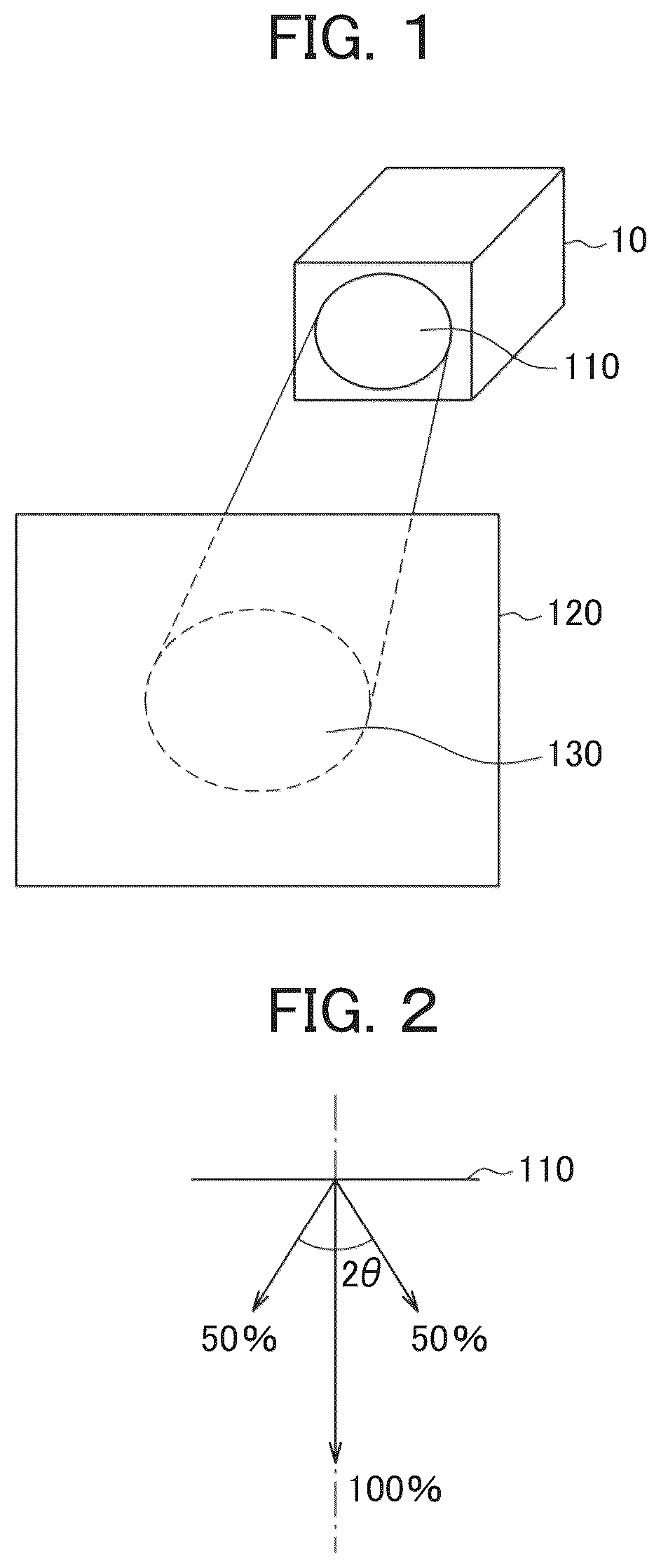
is an example of the lighting device 10 , which is used for a spot light. The light from the lighting device 10 is collimated; a spot light 130 is emitted from the emitting surface 110 , and applied to an incident surface 120 . The light distribution angle is controlled as e.g. 12 degrees to acquire a spot light 130 .
defines the light distribution angle. shows e.g. that a spot light is applied to the floor from a light emitting surface 110 disposed on the ceiling. The light intensity is largest at the normal direction to the light emitting surface 110 ; the light intensity decreases according to the polar angle becoming larger. The light distribution angle is defined as 2θ provided the intensity along the normal direction is 100%, and the intensity along the polar angle θ is 50%. In normally collimated light, the light distribution angle is required as 12 degrees or less.
Conventionally, a parabolic mirror 200 has been used to acquire such a collimated light. is a plan view of the lighting device using a parabolic mirror 200 ; is a cross sectional view of the lighting device of . In , an LED 20 is set at the center of the parabolic mirror 200 . The LED 20 is set e.g. on a PCB substrate 30 . The LED 20 is a high brightness LED, which becomes high temperature; thus, the LED 20 is set on a heat sink 300 . A part of the heat sink 300 , which is set at the rear of the parabolic mirror 200 , is visible in .
is a cross sectional view of along the line A-A. In , the LED 20 is disposed at the bottom surface of the parabolic mirror 200 . The lights emitted from the LED 20 , except the light emitted in the optical axis direction, reflect at the parabolic mirror and become parallel to the optical axis. The parabolic mirror 200 , however, needs to be as high as h1 for enough collimating function. The height h1 of the parabolic mirror 200 needs to be about 60 mm to acquire the light distribution angle of about 12 degrees. Actually, since the height h2 of the heat sink 300 is added, the total height of the lighting device becomes 80 mm or more. In the meantime, in the lighting device of , one LED, which constitutes the light source, needs to be supplied with a large power; consequently, the heat generation in the LED becomes large, thus, the heat sink is indispensable.
The purpose of the present invention is to realize the lighting device, which can emit collimated light, of thin and comparatively low power consumption. The present invention is explained by the following embodiments.
Embodiment 1
is a plan view of the lighting device 10 according to embodiment 1; is a cross sectional view of along the line B-B. As depicted in , a plan view of the lighting device is circular; and a prism sheet 14 is disposed at the upper most surface of the lighting device. Each of the optical components is disc shaped, and is inserted in an axis 111 of a metal frame 11 , which has a central axis 111 and a circular flange 112 . A flexible wiring substrate 21 , on which LEDs are installed, is disposed to surround the axis 111 of the frame 11 ; the flexible wiring substrate 21 is adhered to the axis 111 of the frame 11 through a heat conductive sheet 25 . The heat generated by the LED 20 conducts to the axis 111 of the frame 11 through the heat conductive sheet 25 , and is dissipated into the flange 112 of the frame 11 . An outer size dd of the lighting device 10 is e.g. 98 mm.
is a cross sectional view of along the line B-B. In , a reflecting sheet 12 , a bottom light guide 13 , a top light guide 14 , and a prism sheet 15 are superposed in this order on the flange 112 of the frame 11 formed from metal. Each of those optical components has a hole at the center to be adapted to the axis 111 of the frame 11 . The flexible wiring substrate 21 , on which LEDs are installed, is adhered surrounding the axis 111 of the frame 11 . A part of the flexible wiring substrates 21 extends to back of the flange 112 of the frame 11 through a cut out formed in the flange 112 of the frame 11 . The flexible wiring substrate 21 and the axis 111 of the frame 11 are adhered to each other by the heat conductive tape 25 , which has a superior heat conductivity.
In , the reflection sheet 12 is set on the flange 112 . An ESR (Enhanced Specular Reflector) of 3 M Company, for example, can be used as the reflection sheet 12 ; a thickness is e.g. 70 micron. One of the features of the present invention is to dispose the bottom light guide 13 and the top light guide 14 on the reflecting sheet 12 . The LEDs 20 are disposed corresponding to the inner side surfaces of the light guides 13 and 14 .
The arrows show light passes of the light emitted from each of the LEDs 20 . The light entered in the top light guide 14 and in the bottom light guide 13 repeats reflections, and eventually goes upper direction, namely, to the emitting surface. In , since the light reflects also at an interface between the top light guide 14 and the bottom light guide 13 , the light can be guided to the emitting surface more efficiently than a case when there is only one light guide. Detailed explanation of the light guide is made later.
The other feature of the present invention is, as shown in and , the plurality of LEDs 20 are disposed at inner side walls of the top light guide 14 and the bottom light guide 13 ; thus, temperature rise of each of the LEDs 20 are suppressed, consequently, a decrease in the light emitting efficiency is suppressed because power consumption of each of the LEDs 20 is decreased, and the temperature rise of each of the LEDs 20 is decreased. In , the light emitting from the major surface of the top light guide 14 is further collimated by the prism sheet 15 disposed on the top light guide 14 , and is directed to align with the normal line of the emitting surface of the lighting device 10 .
is an exploded perspective view of the structure of the lighting device explained in . The flexible wiring substrate 21 , installed with LEDs 20 , surrounds and is adhered to the axis 111 of the frame 11 . is a cross sectional view of along the line C-C, which is a detailed cross sectional view at the vicinity of the axis 111 of the frame 11 . The LEDs 20 are disposed in two tiers on the flexible wiring substrate 21 , and are disposed to oppose to the top light guide 14 and the bottom light guide 13 . The LED 20 becomes high temperature, however, the heat of the LED 20 is dissipated to the axis 111 of the frame 11 , which is made of metal, through a thin flexible wiring substrate 25 .
Back to , the axis 111 of the frame 11 is inserted in the holes of the reflection sheet 12 , the bottom light guide 13 and the top light guide 14 . is a plan view of the top light guide 14 and the bottom light guide 13 . Pattern areas 131 and 141 , in which prism arrays are formed, and no pattern areas 132 and 142 , in which prism patterns are not formed, are formed in each of the bottom light guide 13 and the top light guide 14 . When the bottom light guide 13 and the top light guide 14 are superposed, the pattern area 131 of the bottom light guide 13 overlaps the no pattern area 142 of the top light guide 14 ; and the no patter area 132 of the bottom light guide 13 overlaps the pattern area 141 of the top light guide 14 .
A is a plan view of the structure of prism array formed on the surface of bottom light guide 13 . In A , the area 131 of prism array and the area 132 of no prism array are disposed alternatively in a circumferential direction. The prism array formed on the top surface of the bottom light guide 13 (herein after may be called as a major surface) is formed in radially in radius direction; the prism array formed on the bottom surface of the bottom light guide 13 (herein after may be called as a back surface) is formed in concentrically. The LEDs 20 are disposed at the inner wall corresponding to the region where the prism arrays are formed.
B is a cross sectional view of A along the line E-E, which is a cross sectional view of the prism array formed on a surface of the major surface of the light guide 13 . The prism array of the major surface is a pattern radially extending from the center; therefore, a pitch pt of the prism array changes according to the locations. A thickness tg of the light guide is e.g. 1.5 mm; a height ht of prism array is e.g. 0.1 μm; the apex angle θt is e.g. 90 degrees.
C is a cross sectional view of A along the line F-F, which is a cross sectional view of the prism array formed on the back surface of the light guide 13 . The prism array of the back surface is a pattern formed in concentrically. A pitch of the concentric circles is e.g. 0.1 μm; a height hb of the prism is e.g. 0.02 μm; the apex angle θb is e.g. 90 degrees. The height hb of the prism formed on the bottom surface of the prism 13 is lower than a height ht of the prism formed on the top surface of the prism 13 . However, a height and a pitch of the prism array formed both surfaces of the top and the bottom of the light guide 13 , are much smaller compared with a height and a pitch of the prism array formed at the surface of the prism sheet 15 , which is explained later. Therefore, denser prism arrays are formed on the major surface and the back surface of the light guide 13 . In the meantime, it is explained that the prism arrays formed on light guide 13 are formed by projections, however, the prism arrays formed by V shaped grooves also can perform the same effects.
The above explanation is made for the bottom light guide 13 ; however, the same figure can be applied to the top light guide 14 . When the bottom light guide 13 and the top light guide 14 are assembled, the bottom light guide 13 and the top light guide 14 are deviated from each other in circumferential direction so that the pattern area of the top light guide 14 superposes the no pattern area of the bottom light guide 13 .
is a plan view of brightness pattern of the major surface of the light guide 13 when the LED 20 , which is disposed at the inner wall of the light guide 13 , is lighted on. In , the LED 20 is disposed corresponding to the pattern area 131 of the light guide 13 . The light emitted from the LED 20 disposed at the side wall of the hole of the light guide 13 is emitted from the pattern area 131 of the major surface by the reflection sheet 12 , and the prism arrays formed on the major surface and the back surface of the light guide 13 .
In , b1, b2, and b3 are contour of the brightness; b1 is the place of brightest. The feature of is that the light from the LED 20 is emitted only from the corresponding pattern area 131 of the light guide 13 . That is to say, the light from the LED 20 is efficiently collected to the pattern area 131 of the major surface according to prism arrays formed on the major surface and the back surface of the light guide 13 . The above behavior is the same in the top light guide 14 .
is a plan view of brightness distributions at the major surfaces of the top light guide 14 and the bottom light guide 13 when the LEDs 20 are lighted on. In , the hatched parts in the top light guide 14 and the bottom light guide 13 are bright areas, namely the place where the LEDs 20 are disposed. In , the LEDs 20 disposed at the top light guide 14 and LEDs 20 disposed at the bottom light guide 13 are different ones.
is a brightness distribution when the top light guide 14 and the bottom light guide 13 are superposed. The top light guide 14 and the bottom light guide 13 are superposed as that a bright area from which the light from the LED 20 is emitted and a dark area from which the light from the LED 20 is not emitted overlap; therefore, the light is emitted uniformly from the major surface of the light guide 14 . is a perspective view of the disposition of the LEDs 20 , which are disposed at the inner wall of the bottom light guide 13 and the inner wall of the top light guide 14 . The LEDs 20 are disposed circumferentially in an upper tier and in a lower tier; the LEDs 20 in the upper tier and the LEDs 20 in the lower tier are disposed alternative in azimuth direction. According to the above disposition, more LEDs 20 can be disposed; thus, power consumption of each of LEDs can be suppressed, and heat generation can be mitigated.
A is a plan view of a prism sheet 15 , which is disposed on the top light guide 14 . The prism sheet 15 is a so called a reverse prism sheet, in which the prism array is formed at the surface opposing to the top light guide 14 . In , the prism array is formed concentrically; therefore, the light emitting from the top light guide 14 is directed parallel to the normal direction of the major surface of the prism sheet 15 .
B is a cross sectional view of A along the line D-D, which is a cross sectional view to show a shape of the prism array. In B , a thickness tp of the prism sheet 15 is e.g. 200 μm, a depth vd of the V shaped groove is 75 μm, an apex angle θp is e.g. 66 degrees, a pitch pp is e.g. 100 μm. As described above, the height and the pitch formed in the prism sheet 15 are much larger compared with the heights and the pitches of the prism arrays formed at the major surfaces and the back surfaces of the bottom light guide 13 and the top light guide 14 .
In the lighting device 10 explained above has the axis 111 of the frame 11 at the center area, and the light is not emitted from this area. Therefore, the luminous distribution is measured in the structure shown in . shows that light is projected to the ceiling 120 from the lighting device 10 . A diameter of the emitting surface of the lighting device 10 is 98 mm, a distance from the emitting surface to the irradiated surface 120 is 2000 mm.
is an illuminance distribution of the light spot. As shown in the top figure of , the illuminance distribution is approximately concentric; and as shown by the bottom figure of , the luminance intensity is approximately in a normal distribution. As described above, even there is a region which does not emit light at the center of the lighting device 10 , this region does not influence the projected light spot. In the meantime, the light distribution of the lighting device of is approximately 12 degrees.
is a table, which compares various lighting devices to get the same illuminance. The compared structure (Comparison), in which the lighting device has a different structure from the embodiment, uses one LED. The structures (1) to (4) in , which have structure of the present invention, changes the number or characteristics of the LEDs. The power consumption and heat generation are compared in those structures in .
In , illuminous flux/LED is a flux per one LED; necessary numbers of LEDs means the number of the LEDs per one lighting device to get a necessary illuminance; power consumption/LED (W) is a power consumption per one LED; total power consumption (W) is (power consumption per one LED)×(necessary number of LEDs); colorific value (Kcal) is total power consumption (W) converted to calorie.
As shown , according to the present invention, the power consumption as the total LEDs can be made smaller compared with the case in which one LED is used as the light source. In addition, temperature rise of each of the LEDs can be made lower, thus, a decrease in light emitting efficiency can be suppressed; further, since the heat generation can be suppressed as a lighting device in total, a heat sink, like a fin, etc., can be omitted; in addition, a thickness of the lighting device can be made thin. As to the light distribution angle, approximately 12 degrees can be attainable.
Embodiment 2
Embodiment 2 relates to the structure to control the outgoing light by setting liquid crystal lens at the emitting surface of the lighting device. A through 19 C are conceptual view relating to a function of the liquid crystal lens. C is a cross sectional view of the lighting device 10 . In C , the emitting surface 110 is divided into the regions of A, B, C and so forth. The light having a predetermined light distribution angle is emitted from each of the regions.
B shows an example of illuminance at a distance dz from the emitting surface 110 in C . The vertical axis is an illuminance from each of areas A, B, C, and the like; Ad, Bd, Cd, and so forth are distribution of illuminance, which resembles to a normal distribution. A is a summation of illuminance from each of the areas depicted in B . The vertical axis in A is a summation of illuminance at the irradiated surface 120 from each of the areas at the emitting surface area 110 . A shows the total illuminance distribution at the irradiated surface 120 , a distance dz away from the emitting surface 110 , is trapezoidal.
Embodiment 2 is a structure to set a liquid crystal lens at the emitting surface 110 to control the illuminance distribution at the irradiated surface 120 , in other words, to change the illuminance distribution Ad, Bd, Cd, and so forth at the irradiated plane 120 , a distance dz away from the emitting surface 110 , by changing emitting light distribution at the regions A, B, C and so forth at the emitting surface 110 in B .
is a plan view of the lighting device 10 according to embodiment 2. is the same as of embodiment 1 except an upper polarizing plate 70 for the liquid crystal lens is set at the upper most surface in . is a cross sectional view of along the line G-G. In , the structures from the frame 11 to prism sheet 15 are the same as . In , a lower polarizing plate 60 is set on the upper prism sheet 15 ; a lower liquid crystal lens 40 is set on the lower polarizing plate 60 ; an upper liquid crystal lens 50 is set on the lower liquid crystal lens 40 ; and the upper polarizing plate 70 is set on the upper liquid crystal lens 50 .
is a cross sectional view of the lower liquid crystal lens 40 and the upper liquid crystal lens 50 . In the lower liquid crystal lens 40 , a first substrate 41 and a second substrate 42 are adhered to each other at the periphery through a seal material 45 ; a liquid crystal 43 is sealed thereinside. In the upper liquid crystal lens 50 , a third substrate 51 and a fourth substrate 52 are adhered to each other at the periphery through a seal material 55 ; a liquid crystal 53 is sealed thereinside.
is a plan view of a second electrode 421 formed on the second substrate 42 of the lower liquid crystal lens 40 . is a plan view of a first electrode 411 formed on the first substrate 41 of the lower liquid crystal lens 40 . In , the first electrodes 411 extend in y direction and are arranged in x direction.
is a plan view of a third electrode 511 formed on the third substrate 51 of the upper liquid crystal lens 50 . The third electrodes 511 extend in x direction and are arranged in y direction. The fourth electrode formed on the fourth substrate 52 is the same as the second electrode 421 of the lower liquid crystal lens 40 in . All the electrodes from the first electrode through the fourth electrode are made of transparent conductive film as e.g. ITO (Indium Tin Oxide).
A through 26 C are cross sectional views to explain function of the liquid crystal lens, which corresponds to e.g. cross sectional view along the line H-H of . A through C are explained for the lower liquid crystal lens 40 ; however, the function is the same for the upper liquid crystal lens 50 . In A , the comb shaped electrode 411 is formed on the first substrate 41 and the plane electrode 421 is formed on the second substrate 42 . Liquid crystal molecules 431 are arranged parallel to the substrate if field is not applied between the electrodes. In other words, it is in a so called homogeneous alignment.
B is an example of lines of forces LF when a voltage is applied between the comb shaped electrode 411 of the first substrate 41 and the plane electrode 421 of the second substrate 42 . C is a cross sectional view which shows alignment of the liquid crystal molecules 431 when a voltage is applied to the first electrode 411 . In C , the liquid crystal molecules 431 align along the lines of forces LF; consequently, the distribution in refraction is generated, thus, liquid crystal lens is formed. Such a lens is referred to as the distributed refractive index type lens GRIN (Gradient Index Lens).
is an example of the distributed refractive index type lens. The vertical axis of is refractive index. The refractive index is minimum on the first electrode 411 , which is a comb electrode; the refractive index is maximum at the intermediate position between the comb electrodes 411 . shows a normal quadratic curve; however, the distribution of the refractive index can be drastically changed by a voltage between the first electrode 411 and the second electrode 412 , a distance between the comb electrodes of the first electrode 411 , a thickness of the liquid crystal layer 43 , and so forth. Such function is the same in the upper liquid crystal lens 50 . However, the directions of the lens action are perpendicular between in the lower liquid crystal lens 40 and in the upper liquid crystal lens 50 .
A lens pitch of the liquid crystal lens is often determined by division number in the emitting surface. On the other hand, a range in thickness g of the liquid crystal layer in the liquid crystal lens is often limited. is alignments of the liquid crystal molecules 431 and a distribution of the refractive index when the space s between the comb electrodes 411 is substantially larger than a thickness g of the liquid crustal layer. In , the vertical axis is a mean refractive index at each of the positions in the liquid crystal lens; Δneff is a difference of the refractive index in the liquid crystal lens. In the lens in , a lens of small radius of curvature is formed near the comb electrode 411 , and a lens of large radius of curvature is formed at the intermediate position between the comb electrodes 411 .
In some cases, a lens having curvature shown may be used; however, in other cases a lens having curvature of quadratic curve is needed. is a cross sectional view of the liquid crystal lens, in which the lens shape is made in quadratic curve or in smooth curve without changing a pitch of the lens or a thickness of the liquid crystal layer. In , one lens is formed by seven electrodes 411 , and different voltage is applied to each of the electrodes 411 to align the liquid crystal molecules 413 so that refractive index curve becomes a quadratic curve in the liquid crystal lens. In , the voltages are applied as V1>V2>V3>V4. is a plan view of the comb electrodes 411 corresponding to . For example, the region B in corresponds to the region B in C .
In some cases, the direction of the light from the lighting device 10 is intended in a certain direction, not normal to the emitting surface 110 . is an example in which the light from each of the regions A, B, C, and the like is emitted in the direction of ψ to the emitting surface 110 , not normal to the emitting surface 110 . Such function can be attained by shaping each of the liquid crystal lenses asymmetric.
is a plan view of the comb electrodes 411 in which voltages are applied asymmetrically to each of the comb electrodes 411 to make the asymmetric lens. As shown in , the voltages are applied as V1>V2>V3>V4, and V1>V5≠V3, and V1>V6≠V2. As a result, the liquid crystal molecules 431 are aligned to form an asymmetric lens in the cross sectional view of the liquid crystal lens as shown in .
The liquid crystal lens can be realized not only by the homogeneous alignment liquid crystal as shown in A or 29 but also by various other types of liquid crystal devices. A and 33 B are examples that the liquid crystal lens is formed by TN (Twisted Nematic) type liquid crystal. In the TN type, the liquid crystal molecules 431 rotate their alignment direction in 90 degrees between the first substrate 41 and the second substrate 42 .
A is an example in which a voltage is not applied between the first electrode 411 and the second electrode 421 . In this case, the liquid crystal molecules 431 are aligned in parallel to the first substrate 41 or the second substrate 42 ; however, alignment direction of the liquid crystal molecules 431 rotates 90 degrees between a region near the first substrate 41 and a region near the second substrate 42 . B is an example in which a voltage is applied between the first electrode 411 and the second electrode 421 . In this case, the liquid crystal molecules 431 align in vertical direction to the first substrate 41 at directly above the comb electrode 411 , thus, the light is shut. In the intermediate position between the comb electrodes 411 , however, the liquid crystal molecules 431 are not influenced by electric field and maintain rotation of 90 degrees with respect to the alignment direction near the first substrate 41 ; thus, transmittance is not influenced.
When the structure of B is evaluated as a lens, the refractive index is minimum directly above the comb electrode 411 and the refractive index is maximum at the intermediate position between the comb electrodes 411 . Therefore, the distributed refractive index type lens GRIN (Gradient Index Lens) is formed. Various shapes of lenses can be realized by configuring the electrodes as in or even when the lens is formed by TN type liquid crystal.
A to 34 C are cross sectional views in which the liquid crystal lens is formed by applying a voltage between the first electrodes 411 of comb shape. In A , the comb electrodes 411 are formed on the first substrate 41 . On the other hand, no electrode is formed on the second substrate 42 . The liquid crystal lens is constituted by the liquid crystal molecules 431 being aligned by applying a voltage between the comb electrodes 411 , thus, the second electrode 421 is not indispensable. The second electrode 421 is formed by a transparent conductive film as ITO (Indium tin Oxide); however, even a transparent conductive film absorbs or reflects light in certain degree, thus, it is profitable from a view of transmittance of the lens that the second electrode 421 does not exist. The second electrode 421 may be formed on the second substrate 42 e.g. if the shape of the lens is intended to be changed.
B shows lines of forces LF generated by applying a voltage between the comb electrodes 411 . The lines of forces LF are directed vertically to the substrate 41 at the region directly above the comb electrode 411 ; the lines of forces LF are directed in parallel to the substrate 41 at the intermediate position between the comb electrodes 411 . The liquid crystal molecules 431 align in the lines of forces LF.
C is a cross sectional view in which the liquid crystal molecules 431 align in the field that is depicted in B . In C , the refractive index is minimum at directly above the comb electrode 411 and is maximum at the intermediate position between the comb electrodes 411 . Therefore, in this case too, the distributed refractive index type lens GRIN (Gradient Index Lens) is formed.
is a plan view of the first electrode 411 formed on the first substrate 41 . In , the first comb electrode 411 and the second comb electrode 411 are nested. The liquid crystal lens depicted in C is formed by applying a voltage between the first comb electrode 411 and the second comb electrode 411 . Various liquid crystal lenses can be formed by changing a thickness g of the liquid crystal layer, a distance s between the comb electrodes 411 , and a voltage V applied between the comb electrodes 411 .
As described above, lenses of various functions can be formed not only by changing a distance between the electrodes, a thickness of the liquid crystal layer, and an applied voltage between the electrodes, but also by the types of liquid crystal lenses. shows examples to change the illuminance distribution by the liquid crystal lens. is the same structure as B and C , however, only emitting light from the region A is shown. shows that the distribution of the emitting light can be changed in various shapes by the liquid crystal lens set in the region A.
The illuminance distribution Ad1 resembles to the normal distribution; the illuminance distribution Ad2 also resembles to the normal distribution, however, the light is more condensed. The illuminance distribution Ad3 shows a case where the liquid crystal lens is used as a divergence lens to acquire a trapezoidal illuminance distribution. The illuminance distribution Ad4 shows a case where a direction of the axis of the illuminance distribution is deviated in polar angle by making the liquid crystal lens asymmetric.
As explained in A to 19 C , the illuminance distribution on the screen 120 is a summation of the light emitted from each of the regions of the emitting surface 110 . In other words, the illuminance distribution on the irradiating surface 120 can be changed by changing the illuminance distribution from each of the regions, A, B, C, and the like in the emitting surface 110 .
Embodiment 3
is a cross sectional view of the lighting device according to embodiment 3. In embodiment 3, the lens action of the liquid crystal lens is in radial direction. In , only one liquid crystal lens 80 is used, other structures are the same as or 21 . The VA (Vertical alignment) type liquid crystal, namely, the homeotropic alignment liquid crystal, is used to form the liquid crystal lens 80 whose lens action is in radial direction. Rubbing process or photo alignment process to align the liquid crystal molecules 431 in a direction parallel to the alignment film is not necessary in the VA type liquid crystal.
is a cross sectional view of the liquid crystal lens 80 ; is a plan view of a first electrode 811 formed on a first substrate 81 of the liquid crystal lens 80 . corresponds to the cross sectional view of along the line I-I. In the liquid crystal lens of , an electrode is not formed on a second substrate 82 ; the liquid crystal lens is formed by applying voltages between the ring shaped electrodes of the first electrode 811 formed on the first substrate 81 .
In , concentrically formed plural ring shaped electrodes constitute the first electrode 811 . Each of the ring shaped electrodes 811 can be applied with voltages independently. A to 40 C , which correspond to a cross sectional view of along the line J-J, explain the lens function of embodiment 3. A is a cross sectional view in which a voltage is not applied to the first electrode 811 . Since the liquid crystal is homeotropic in this embodiment, the liquid crystal molecules 431 align vertically to the main planes of the first substrate 81 and the second substrate 82 .
B shows lines of forces LF when a voltage is applied between the first electrodes 811 . The line of force LF is directed vertically to the substrate 81 at directly above the comb electrode 811 , and is directed parallel to the substrate 41 at the intermediate position between the comb electrodes 811 . The liquid crystal molecules 431 align along with the line of force LF.
C is a cross sectional view in which the liquid crystal molecules 431 align with the field of B . In C , the refractive index is minimum at directly above the comb electrode 811 and maximum at the intermediate position between the comb electrodes 811 . Therefore, in this case too, the distributed refractive index type lens GRIN (Gradient Index Lens) is formed.
In this case, each of lenses is formed in radial direction of the ring electrodes 811 or in radial direction of the circular first substrate 81 and the circular second substrate 82 . However, the function of each of the lenses in the lighting device is the same as explained in A through 19 C and and so forth.
Embodiment 4
This embodiment relates to the structure in which one liquid crystal lens as a whole is formed in circular liquid crystal lens. through 44 show an example of this structure. In the meantime, a plan view of the lighting device of embodiment 4 is the same as , and a cross sectional view of the lighting device of embodiment 4 is the same as . Further, the lower polarizing plate 60 and upper polarizing plate 70 of and so forth also can be used in embodiment 4. is an example of the first electrode 811 formed on the circular first electrode 81 . Plural ring shaped electrodes formed in concentric constitute the first electrode 811 . The width of the ring electrode of is wider than that of . The leader lines are omitted in .
is an example of a second electrode 821 formed on the circular second substrate 82 . The second electrode 821 is formed in disc shape. The liquid crystal is inserted between the first substrate 81 and the second substrate 82 to constitute the liquid crystal lens. are cross sectional views after the first substrate 81 and the second substrate 82 are assembled; correspond to the cross sectional views of along the line K-K.
is a cross sectional view of the liquid crystal lens in which a voltage is not applied between the disc shaped second electrode 821 and the ring shaped first electrodes 811 . In , since the liquid crystal is homeotropic type, the liquid crystal molecules 431 align vertically to the major surfaces of the first substrate 81 and the second substrate 82 . In , r direction means a radial direction.
is a cross sectional view in which different voltages are applied to the plural ring shaped first electrodes 811 . In , the voltage applied to the second electrode 821 is V1; voltages V1, V2, V3, V4, and V5 are applied to each of the ring shaped first electrodes 811 in order from outside, and V1<V2<V3<V4<V5. The tilting of the liquid crystal molecules 431 becomes larger according to the voltage applied to the first electrode 821 becoming lager; and the liquid crystal molecules 431 align approximately parallel to the first substrate 81 at the center of the first substrate 81 .
When is viewed as a liquid crystal lens, refractive index at the center of the first substrate 81 is maximum where voltage V5 is applied to the first electrode 811 and the liquid crystal molecules 431 align in parallel to the first substrate 81 ; refractive index at the periphery is minimum where voltage V1 is applied to the first electrode 811 and the liquid crystal molecules 431 align vertically to the first substrate 81 . Therefore, from the peripheral portion to the center of the liquid crystal lens, the distributed refractive index type lens GRIN (Gradient Index Lens) is formed. In the liquid crystal lens according to this embodiment, the lens characteristics can be changed according to voltages applied to the plural first electrodes 811 , number of the plural electrodes 811 , thickness g of the liquid crystal layer and so forth.
Embodiment 5
Embodiment 1, shown by , uses two light guides. However, if it is difficult to use two light guides, the two light guides can be substituted by one light guide 16 . is a cross sectional view the lighting device 10 according to this structure. A plan view of is the same as a plan view of . In , LEDs are disposed in two tiers along the inner side wall of the light guide 16 . The configuration of the arrangement of the LEDs 20 are the same as . Therefore, a brightness of the light source is the same as in embodiment 1.
A to 46 C show configuration of the light guide 16 . A is a plan view of the light guide 16 . In A , the first prism array is formed on the major surface radially in radial direction. Unlike A of embodiment 1, the first prism array in this case is formed all around in the circumferential direction. The second prism array is formed on the back surface of the light guide 16 in concentrically. Unlike A of embodiment 1, the second prism array in this case is also formed all around in circumferential direction.
B is a cross sectional view of the first prism array formed on the major surface. This cross sectional view of B is the same as explained in B . C is a cross sectional view of the second prism array formed on the back surface. This cross sectional view of C is the same as explained in C .
Since two light guides exist in the structure of embodiment 1, reflections occur at the interface between the top light guide 14 and the bottom light guide 13 ; however, such reflections at the interface do not occur in this embodiment, since there is only one light guide. Other functions are the same as explained in embodiment 1.
is a cross sectional view of the lighting device, which is intended to be formed extremely thin. A plan view of is the same as of embodiment 1. The structure of differs from the structure of in that the LEDs 20 are arranged in one tier to make the thickness of the light guide 17 thin. The configuration of the first prism array on the major surface and the configuration of the second prism array on the back surface of the light guide 17 in this embodiment can be the same as A to C , or A to C . Other structures of are the same as or .
The structure, which uses two light guides, is explained in embodiment 1; and the structure, which uses one light guide, is explained in embodiment 5. The present invention, however, can be applied to the lighting device which uses three or more light guides. The prism arrays formed on the major surface and the back surface of the light guide can be similar structure as the case of embodiment 1.
Figures (20)
Citations
This patent cites (9)
- US11294223
- US11537001
- US11703710
- US20110019421
- US20180259701
- US20200326470
- US20210054994
- US2004184947
- US2011159435