Gate Structures for Semiconductor Devices
Abstract
A semiconductor device with different gate structure configurations and a method of fabricating the semiconductor device are disclosed. The method includes depositing a high-K dielectric layer surrounding nanostructured channel regions, performing a first doping with a rare-earth metal (REM)-based dopant on first and second portions of the high-K dielectric layer, and performing a second doping with the REM-based dopants on the first portions of the high-K dielectric layer and third portions of the high-K dielectric layer. The first doping dopes the first and second portions of the high-K dielectric layer with a first REM-based dopant concentration. The second doping dopes the first and third portions of the high-K dielectric layer with a second REM-based dopant concentration different from the first REM-based dopant concentration. The method further includes depositing a work function metal layer on the high-K dielectric layer and depositing a metal fill layer on the work function metal layer.
Claims (20)
1. A semiconductor device, comprising: a substrate; a stack of nanostructured layers disposed on the substrate, wherein the stack of nanostructured layers comprises nanostructured channel regions; a gate structure surrounding the nanostructured channel regions, wherein the gate structure comprises: an oxide layer surrounding the nanostructured channel regions, a high-k gate dielectric layer disposed on the oxide layer, wherein the high-k gate dielectric layer comprises metal-based dopants with a graded doping profile that decreases from a top surface of the high-k gate dielectric layer to a bottom surface of the high-k gate dielectric layer, and a metal dipole layer disposed between the oxide layer and the high-k gate dielectric layer; and an epitaxial semiconductor layer surrounding a portion of the stack of nanostructured layers uncovered by the gate structure.
11. A semiconductor device, comprising: a first gate structure, comprising: a first oxide layer, a first gate dielectric layer disposed on the first oxide layer, and a first dipole layer with a first dipole concentration disposed between the first oxide layer and the first gate dielectric layer; and a second gate structure, comprising: a second oxide layer, a second gate dielectric layer disposed on the second oxide layer, and a second dipole layer with a second dipole concentration disposed between the second oxide layer and the second gate dielectric layer, wherein the first and second dipole concentrations are different from each other.
17. A semiconductor device, comprising: an n-type transistor with a first gate structure, the first gate structure comprising: a first oxide layer; a first gate dielectric layer with a first concentration of rare-earth metal-based dopants disposed on the first oxide layer; and a first dipole layer with a first dipole concentration disposed between the first oxide layer and the first gate dielectric layer; and a p-type transistor with a second gate structure, the second gate structure comprising: a second oxide layer; a second gate dielectric layer with a second concentration of the rare-earth metal-based dopants disposed on the second oxide layer, wherein the first and second concentrations are different from each other; and a second dipole layer with a second dipole concentration disposed between the second oxide layer and the second gate dielectric layer, wherein the first and second dipole concentrations are different from each other, wherein the first and second gate structures are gate-all-around gate structures.
Show 17 dependent claims
2. The semiconductor device of claim 1 , wherein the stack of nanostructured layers comprises first and second semiconductor layers arranged in an alternating configuration.
3. The semiconductor device of claim 1 , wherein the metal dipole layer comprises a rare-earth metal.
4. The semiconductor device of claim 1 , wherein the metal dipole layer comprises rare-earth metal ions and oxygen ions.
5. The semiconductor device of claim 1 , wherein the metal dipole layer comprises lanthanum or aluminum.
6. The semiconductor device of claim 1 , wherein the high-k gate dielectric layer comprises rare-earth metal oxide dopants.
7. The semiconductor device of claim 1 , wherein the high-k gate dielectric layer comprises rare-earth metal-based dopants with a graded doping profile across a thickness of the high-k gate dielectric layer.
8. The semiconductor device of claim 1 , wherein the high-k gate dielectric layer comprises a first concentration of rare-earth metal-based dopants and the oxide layer comprises a second concentration of the rare-earth metal-based dopants, and wherein the first concentration is greater than the second concentration.
9. The semiconductor device of claim 1 , wherein the high-k gate dielectric layer comprises aluminum-based dopants.
10. The semiconductor device of claim 1 , wherein the high-k gate dielectric layer comprises aluminum oxide dopants.
12. The semiconductor device of claim 11 , wherein the first gate dielectric layer comprises first metal-based dopants with a first concentration, and wherein the second gate dielectric layer comprises second metal-based dopants with a second concentration that is different from the first concentration.
13. The semiconductor device of claim 11 , wherein the first and second gate dielectric layers comprise rare-earth metal-based dopants.
14. The semiconductor device of claim 11 , wherein the first and second dipole layers comprise rare-earth metal-based dipoles.
15. The semiconductor device of claim 11 , wherein effective work function values of the first and second gate structures are different from each other.
16. The semiconductor device of claim 11 , wherein the first gate structure further comprises a first work function metal layer with a first thickness; and wherein the second gate structure further comprises a second work function metal layer with a second thicknesses that is substantially equal to the first thickness.
18. The semiconductor device of claim 17 , wherein the first dipole layer comprises aluminum-based dipoles with the first dipole concentration; and wherein the second dipole layer comprises aluminum-based dipoles with the second dipole concentration.
19. The semiconductor device of claim 17 , wherein the first and second gate structures surround nanostructured channel regions.
20. The semiconductor device of claim 17 , wherein the first and second dipole layers comprise lanthanum.
Full Description
Show full text →
CROSS-REFERENCE TO RELATED APPLICATIONS
This application is a continuation of U.S. patent application Ser. No. 16/835,987, titled “Gate Structures for Semiconductor Devices,” filed Mar. 31, 2020, which is incorporated by reference herein in its entirety.
BACKGROUND
With advances in semiconductor technology, there has been increasing demand for higher storage capacity, faster processing systems, higher performance, and lower costs. To meet these demands, the semiconductor industry continues to scale down the dimensions of semiconductor devices, such as metal oxide semiconductor field effect transistors (MOSFETs), including planar MOSFETs and fin field effect transistors (finFETs). Such scaling down has increased the complexity of semiconductor manufacturing processes.
BRIEF DESCRIPTION OF THE DRAWINGS
Aspects of this disclosure are best understood from the following detailed description when read with the accompanying figures. It is noted that, in accordance with the common practice in the industry, various features are not drawn to scale. In fact, the dimensions of the various features may be arbitrarily increased or reduced for clarity of discussion.
A, 1 B- 1 C, and 1 D- 1 Q illustrate an isometric view, cross-sectional views, and device characteristics, respectively, of a semiconductor device with different gate structures, in accordance with some embodiments.
is a flow diagram of a method for fabricating a semiconductor device with different gate structures, in accordance with some embodiments.
A- 12 A and 3 B- 12 B illustrate cross-sectional views of a semiconductor device with different gate structures at various stages of its fabrication process, in accordance with some embodiments.
C- 8 D and 11 C- 11 E illustrate device characteristics of a semiconductor device with different gate structures at various stages of its fabrication process, in accordance with some embodiments.
Illustrative embodiments will now be described with reference to the accompanying drawings. In the drawings, like reference numerals generally indicate identical, functionally similar, and/or structurally similar elements.
DETAILED DESCRIPTION
The following disclosure provides many different embodiments, or examples, for implementing different features of the provided subject matter. Specific examples of components and arrangements are described below to simplify the present disclosure. These are, of course, merely examples and are not intended to be limiting. For example, the process for forming a first feature over a second feature in the description that follows may include embodiments in which the first and second features are formed in direct contact, and may also include embodiments in which additional features may be formed between the first and second features, such that the first and second features may not be in direct contact. As used herein, the formation of a first feature on a second feature means the first feature is formed in direct contact with the second feature. In addition, the present disclosure may repeat reference numerals and/or letters in the various examples. This repetition does not in itself dictate a relationship between the various embodiments and/or configurations discussed.
Spatially relative terms, such as “beneath,” “below,” “lower,” “above,” “upper,” and the like may be used herein for ease of description to describe one element or feature's relationship to another element(s) or feature(s) as illustrated in the figures. The spatially relative terms are intended to encompass different orientations of the device in use or operation in addition to the orientation depicted in the figures. The apparatus may be otherwise oriented (rotated 90 degrees or at other orientations) and the spatially relative descriptors used herein may likewise be interpreted accordingly.
It is noted that references in the specification to “one embodiment,” “an embodiment,” “an example embodiment,” “exemplary,” etc., indicate that the embodiment described may include a particular feature, structure, or characteristic, but every embodiment may not necessarily include the particular feature, structure, or characteristic. Moreover, such phrases do not necessarily refer to the same embodiment. Further, when a particular feature, structure or characteristic is described in connection with an embodiment, it would be within the knowledge of one skilled in the art to effect such feature, structure or characteristic in connection with other embodiments whether or not explicitly described.
It is to be understood that the phraseology or terminology herein is for the purpose of description and not of limitation, such that the terminology or phraseology of the present specification is to be interpreted by those skilled in relevant art(s) in light of the teachings herein.
As used herein, the term “etch selectivity” refers to the ratio of the etch rates of two different materials under the same etching conditions.
As used herein, the term “high-k” refers to a high dielectric constant. In the field of semiconductor device structures and manufacturing processes, high-k refers to a dielectric constant that is greater than the dielectric constant of SiO 2 (e.g., greater than 3.9).
As used herein, the term “p-type” defines a structure, layer, and/or region as being doped with p-type dopants, such as boron.
As used herein, the term “n-type” defines a structure, layer, and/or region as being doped with n-type dopants, such as phosphorus.
As used herein, the term “nanostructured” defines a structure, layer, and/or region as having a horizontal dimension (e.g., along an X- and/or Y-axis) and/or a vertical dimension (e.g., along a Z-axis) less than, for example, 100 nm.
As used herein, the term “n-type work function metal (nWFM)” defines a metal or a metal-containing material with a work function value closer to a conduction band energy than a valence band energy of a material of a FET channel region. In some embodiments, the term “n-type work function metal (nWFM)” defines a metal or a metal-containing material with a work function value less than 4.5 eV.
As used herein, the term “p-type work function metal (pWFM)” defines a metal or a metal-containing material with a work function value closer to a valence band energy than a conduction band energy of a material of a FET channel region. In some embodiments, the term “p-type work function metal (pWFM)” defines a metal or a metal-containing material with a work function value equal to or greater than 4.5 eV.
As used herein, the term “effective work function value” defines a difference between a work function value of a WFM layer of a FET gate structure and a potential difference induced across a dipole layer formed between a high-k dielectric layer and an interfacial layer of the FET gate structure.
In some embodiments, the terms “about” and “substantially” can indicate a value of a given quantity that varies within 5% of the value (e.g., ±1%, ±2%, ±3%, ±4%, ±5% of the value).
The fin structures disclosed herein may be patterned by any suitable method. For example, the fin structures may be patterned using one or more photolithography processes, including double-patterning or multi-patterning processes. Generally, double-patterning or multi-patterning processes combine photolithography and self-aligned processes, allowing patterns to be created that have, for example, pitches smaller than what is otherwise obtainable using a single, direct photolithography process. For example, in some embodiments, a sacrificial layer is formed over a substrate and patterned using a photolithography process. Spacers are formed alongside the patterned sacrificial layer using a self-aligned process. The sacrificial layer is then removed, and the remaining spacers may then be used to pattern the fin structures.
The required gate voltage—the threshold voltage Vt—to turn on a field effect transistor (FET) can depend on the semiconductor material of the FET channel region and the work function value of a WFM layer of a gate structure of the FET. For example, for an n-type FET (NFET), reducing the difference between the work function value of the nWFM layer of the NFET gate structure and the conduction band energy of the material (e.g., 4.1 eV for Si or 3.8 eV for SiGe) of the NFET channel region can reduce the NFET threshold voltage. For a p-type FET (PFET), reducing the difference between the work function value of the pWFM layer of the PFET gate structure and the valence band energy of the material (e.g., 5.2 eV for Si or 4.8 eV for SiGe) of the PFET channel region can reduce the PFET threshold voltage. The threshold voltage of the FET gate structure can depend on the thickness and/or material composition of each of the layers of the FET gate structures. As such, FETs can be manufactured with different threshold voltages by adjusting the thickness and/or material composition of the gate structures.
Due to the increasing demand for low power portable devices, there is an increasing demand for FETs with low threshold voltages, such as threshold voltages lower than 100 mV. One way to achieve such low threshold voltage in FETs can be by using work function metal (WFM) layer(s) with thickness(es) greater than about 4 nm (e.g., about 5 nm to about 10 nm) in the gate structures. However, the thickness(es) of the WFM layer(s) in the gate structures can be constrained by the gate structure geometries of the FETs. For example, in gate-all-around (GAA) FETs, the thickness of the WFM layer(s) can be constrained by the spacing between the nanostructured channel regions of the GAA FETs. Also, depositing such thick WFM layer(s) can become increasingly challenging with the continuous scaling down of FETs (e.g., GAA FETs).
The present disclosure provides example structures of FETs (e.g., finFETs or GAA FETs) with gate structures of different effective work function values to provide different and/or low threshold voltages and example methods of forming such FETs on a same substrate. The example methods form FETs of different conductivity types with different effective work function values without increasing the thicknesses of the WFM layers. These example methods can be less complicated and more cost-effective in manufacturing reliable gate structures in FETs with nanostructured channel regions and with different and/or low threshold voltages than other methods of forming FETs with similar channel dimensions and threshold voltages on the same substrate. In addition, these example methods can form FET gate structures with smaller dimensions (e.g., thinner gate stacks) than other methods of forming FETs with similar threshold voltages.
In some embodiments, NFETs and PFETs with different gate structure configurations can be selectively formed on the same substrate. To achieve NFETs and PFETs with different and/or low threshold voltages, high-K (HK) gate dielectric layers of NFET and PFET gate structures can be doped with different concentrations of rare-earth metal (REM)-based dopants. The different concentrations of REM-based dopants can generate dipole layers with varying dipole concentrations in the NFET and PFET gate structures. Tuning the dipole concentrations can tune the effective work function values of the NFET and PFET gate structures and as a result, adjust the threshold voltages of the NFETs and PFETs. As such, NFETs and PFETs with different and/or low threshold voltages can be obtained without increasing the thickness of the WFM layers.
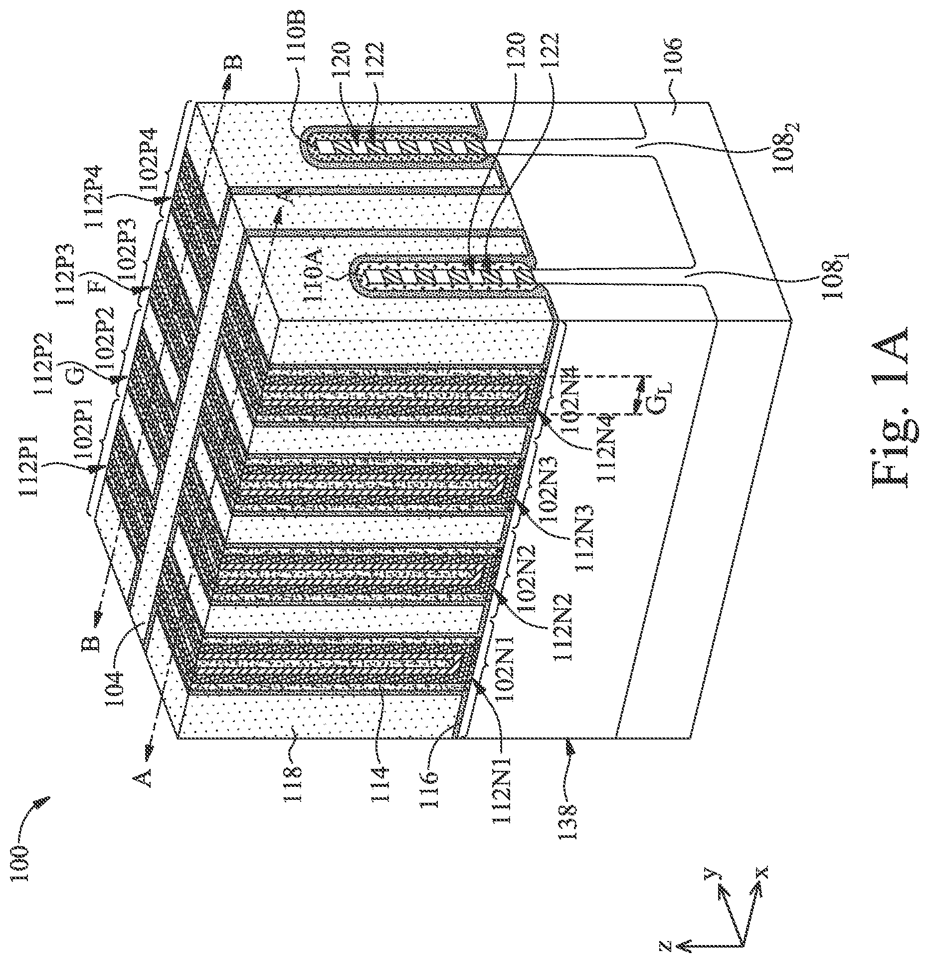
A semiconductor device 100 having NFETs 102 N 1 - 102 N 4 and PFETs 102 P 1 - 102 P 4 is described with reference to A- 1 Q , according to some embodiments. A illustrates an isometric view of semiconductor device 100 , according to some embodiments. B- 1 C illustrate cross-sectional views along lines A-A and B-B of semiconductor device 100 of A , respectively, according to some embodiments. D- 1 Q illustrate devices characteristics of semiconductor device 100 , according to some embodiments. Even though eight FETs are discussed with reference to A- 1 Q , semiconductor device 100 can have any number of FETs. The discussion of elements of NFETs 102 N 1 - 102 N 4 and PFETs 102 P 1 - 102 P 4 with the same annotations applies to each other, unless mentioned otherwise. The isometric view and cross-sectional views of semiconductor device 100 are shown for illustration purposes and may not be drawn to scale.
Referring to A- 1 C , NFETs 102 N 1 - 102 N 4 and PFETs 102 P 1 - 102 P 4 can be formed on a substrate 106 . Substrate 106 can be a semiconductor material such as, but not limited to, silicon. In some embodiments, substrate 106 can include a crystalline silicon substrate (e.g., wafer). In some embodiments, substrate 106 can include (i) an elementary semiconductor, such as germanium (Ge); (ii) a compound semiconductor including silicon carbide (SiC), silicon arsenide (SiAs), gallium arsenide (GaAs), gallium phosphide (GaP), indium phosphide (InP), indium arsenide (InAs), indium antimonide (InSb), and/or a III-V semiconductor material; (iii) an alloy semiconductor including silicon germanium (SiGe), silicon germanium carbide (SiGeC), germanium stannum (GeSn), silicon germanium stannum (SiGeSn), gallium arsenic phosphide (GaAsP), gallium indium phosphide (GaInP), gallium indium arsenide (GaInAs), gallium indium arsenic phosphide (GaInAsP), aluminum indium arsenide (AlAs), and/or aluminum gallium arsenide (AlGaAs); (iv) a silicon-on-insulator (SOI) structure; (v) a silicon germanium (SiGe)-on insulator structure (SiGeOI); (vi) germanium-on-insulator (GeOI) structure; or (vii) a combination thereof. Further, substrate 106 can be doped depending on design requirements (e.g., p-type substrate or n-type substrate). In some embodiments, substrate 106 can be doped with p-type dopants (e.g., boron, indium, aluminum, or gallium) or n-type dopants (e.g., phosphorus or arsenic).
NFETs 102 N 1 - 102 N 4 and PFETs 102 P 1 - 102 P 4 can include fin structures 108 1 - 108 2 extending along an X-axis, epitaxial fin regions 110 A- 110 B, gate structures 112 N 1 - 112 N 4 and 112 P 1 - 112 P 4 (also referred to as “gate-all-around (GAA) structures 112 N 1 - 112 N 4 and 112 P 1 - 112 P 4 ”), respectively, inner spacers 142 , and gate spacers 114 .
As shown in B- 1 C , fin structure 108 1 can include a fin base portion 108 A 1 and a stacked fin portion 108 B 1 disposed on fin base portion 108 A 1 and fin structure 108 2 can include a fin base portion 108 A 2 and a stacked fin portion 108 B 2 disposed on fin base portion 108 A 2 . In some embodiments, fin base portions 108 A 1 - 108 A 2 can include material similar to substrate 106 . Fin base portions 108 A 1 - 108 A 2 can be formed from photolithographic patterning and etching of substrate 106 . Stacked fin portions 108 B 1 - 108 B 2 can include first and second semiconductor layers 120 and 122 stacked in an alternating configuration. Each first semiconductor layer 120 of stacked fin portion 108 B 1 can have (i) nanostructured regions 120 A (shown in B ) underlying epitaxial fin regions 110 A, and (ii) nanostructured channel regions 120 B (shown in B ) wrapped around by gate structures 112 N 1 - 112 N 4 . Each second semiconductor layer 122 of stacked fin portion 108 B 2 can have (i) nanostructured regions 122 A (shown in C ) underlying epitaxial fin regions 110 B, and (ii) nanostructured channel regions 122 B (shown in C ) wrapped around by gate structures 112 P 1 - 112 P 4 .
First and second semiconductor layers 120 and 122 can include semiconductor materials different from each other. In some embodiments, first and second semiconductor layers 120 and 122 can include semiconductor materials with oxidation rates and/or etch selectivity different from each other. In some embodiments, first and second semiconductor layers 120 and 122 can include semiconductor materials similar to or different from substrate 106 . First and second semiconductor layers 120 and 122 can include (i) an elementary semiconductor, such as silicon or germanium; (ii) a compound semiconductor including a III-V semiconductor material; (iii) an alloy semiconductor including SiGe, germanium stannum, or silicon germanium stannum; or (iv) a combination thereof.
In some embodiments, first semiconductor layers 120 can include Si, SiAs, silicon phosphide (SiP), SiC, or silicon carbon phosphide (SiCP) for NFETs 102 N 1 - 102 N 4 and second semiconductor layers 122 can include SiGe, silicon germanium boron (SiGeB), germanium boron (GeB), silicon germanium stannum boron (SiGeSnB), or a III-V semiconductor compound for PFETs 102 P 1 - 102 P 4 . In some embodiments, first and semiconductor layers 120 and 122 can each include Si, SiAs, SiP, SiC, or SiCP for NFETs 102 N 1 - 102 N 4 or SiGe, SiGeB, GeB, SiGeSnB or a III-V semiconductor compound for PFETs 102 P 1 - 102 P 4 . In some embodiments, first and second semiconductor layers 120 and 122 can include materials similar to each other for NFETs 102 N 1 - 102 N 4 and PFETs 102 P 1 - 102 P 4 . Though rectangular cross-sections of nanostructured channel regions 120 B and 122 B are shown in B , nanostructured channel regions 120 B and 122 B can have cross-sections of other geometric shapes (e.g., circular, elliptical, triangular, or polygonal).
Referring to A- 1 C , epitaxial fin regions 110 A can be grown wrapped around stacked fin portion 108 B 1 . Similarly, epitaxial fin regions 110 B can be grown wrapped around stacked fin portion 108 B 2 . In some embodiments, epitaxial fin regions 110 A- 110 B can be grown on fin base portions 108 A 1 - 108 A 2 , instead of being wrapped around stacked fin portion 108 B 1 - 108 B 2 , respectively. Epitaxial fin regions 110 A- 110 B along with their underlying nanostructured regions 120 A and 122 A can form source/drain (S/D) regions 126 A- 126 B, respectively.
Epitaxial fin regions 110 A- 110 B can include epitaxially-grown semiconductor materials similar to or different from each other. In some embodiments, the epitaxially-grown semiconductor material can include the same material or a different material from the material of substrate 106 . Epitaxial fin regions 110 A- 110 B can be n- and p-type, respectively. In some embodiments, n-type epitaxial fin regions 110 A can have materials with SiAs, SiC, or SiCP. P-type epitaxial fin regions 110 B can include SiGe, SiGeB, GeB, SiGeSnB, a III-V semiconductor compound, or a combination thereof.
Gate structures 112 N 1 - 112 N 4 and 112 P 1 - 112 P 4 can be multi-layered structures and can be wrapped around nanostructured channel regions 120 B and 122 B, respectively, for which gate structures 112 N 1 - 112 N 4 and 112 P 1 - 112 P 4 can be referred to as “gate-all-around (GAA) structures” or “horizontal gate-all-around (HGAA) structures,” and NFETs 102 N 1 - 102 N 4 and PFETs 102 P 1 - 102 P 4 can be referred to as “GAA FETs 102 N 1 - 102 N 4 and 102 P 1 - 102 P 4 ” or “GAA NFETs 102 N 1 - 102 N 4 and PFETs 102 P 1 - 102 P 4 ,” respectively.
Referring to A- 1 C , gate structures 112 N 1 - 112 N 4 and 112 P 1 - 112 P 4 can include interfacial oxide layers 127 , high-k (HK) gate dielectric layers 128 N 1 - 128 N 4 and 128 P 1 - 128 P 4 , gate WFM layers 130 , and gate metal fill layers 132 . Even though B- 1 C show that all the layers of gate structures 112 N 1 - 112 N 4 and 112 P 1 - 112 P 4 are wrapped around nanostructured channel regions 120 B and 122 B, respectively, nanostructured channel regions 120 B and 122 B can be wrapped around by at least interfacial oxide layers 127 and HK gate dielectric layers 128 N 1 - 128 N 4 and 128 P 1 - 128 P 4 to fill the spaces between adjacent nanostructured channel regions 120 B and 122 B. As such, nanostructured channel regions 120 B and 122 B can be electrically isolated from each other, respectively, to prevent shorting between gate structures 112 N 1 - 112 N 4 and 112 P 1 - 112 P 4 and S/D regions 126 A- 126 B during operation of NFETs 102 N 1 - 102 N 4 and PFETs 102 P 1 - 102 P 4 , respectively. In some embodiments, instead of all the layers of gate structures 112 N 1 - 112 N 4 and 112 P 1 - 112 P 4 being wrapped around nanostructured channel regions 120 B and 122 B, respectively, nanostructured channel regions 120 B and 122 B can be wrapped around by at least interfacial oxide layers 127 , HK gate dielectric layers 128 N 1 - 128 N 4 and 128 P 1 - 128 P 4 , and gate WFM layers 130 to fill the spaces between adjacent nanostructured channel regions 120 B and 122 B.
Interfacial oxide layers 127 can be disposed on nanostructured channel regions 120 B and 122 B and can include silicon oxide and a thickness ranging from about 0.5 nm to about 1.5 nm. Each of HK gate dielectric layers 128 N 1 - 128 N 4 and 128 P 1 - 128 P 4 can have a thickness (e.g., about 1 nm to about 3 nm) that is about 2 to 3 times the thickness of interfacial oxide layers 127 and can include (i) a high-k dielectric material, such as hafnium oxide (HfO 2 ), titanium oxide (TiO 2 ), hafnium zirconium oxide (HfZrO), tantalum oxide (Ta 2 O 3 ), hafnium silicate (HfSiO 4 ), zirconium oxide (ZrO 2 ), zirconium silicate (ZrSiO 2 ), (ii) a high-k dielectric material having oxides of lithium (Li), beryllium (Be), magnesium (Mg), calcium (Ca), strontium (Sr), scandium (Sc), yttrium (Y), zirconium (Zr), aluminum (Al), lanthanum (La), cerium (Ce), praseodymium (Pr), neodymium (Nd), samarium (Sm), europium (Eu), gadolinium (Gd), terbium (Tb), dysprosium (Dy), holmium (Ho), erbium (Er), thulium (Tm), ytterbium (Yb), or lutetium (Lu), or (iii) a combination thereof.
In some embodiments, HK gate dielectric layers 128 N 1 - 128 N 3 and 128 P 1 - 128 P 3 can include rare-earth metal (REM)-based dopants. The REM-based dopants can include oxides of REM, such as Lanthanum oxide (La 2 O 3 ), Yttrium oxide (Y 2 O 3 ), Cerium oxide (CeO 2 ), Ytterbium oxide (Yb 2 O 3 ), Erbium oxide (Er 2 O 3 ), or a combination thereof. The REM-based dopant concentration in HK gate dielectric layers 128 N 1 - 128 N 3 and 128 P 1 - 128 P 3 can be similar or different from each other. In some embodiments, HK gate dielectric layers 128 N 1 and 128 P 1 can have REM-based dopant concentration C 1 , HK gate dielectric layers 128 N 2 and 128 P 2 can have REM-based dopant concentration C 2 , and HK gate dielectric layers 128 N 3 and 128 P 3 can have REM-based dopant concentration C 3 . In some embodiments, concentration C 1 is greater than concentrations C 2 and/or C 3 . In some embodiments, concentration C 1 is greater than concentrations C 2 and C 3 , and concentration C 2 is greater than concentration C 3 . In some embodiments, concentration C 1 is greater than concentrations C 2 and C 3 , and concentration C 3 is greater than concentration C 2 . In some embodiments, HK gate dielectric layers 128 N 4 and 128 P 4 can have REM-based dopant concentration C 4 , which can be equal to zero. In some embodiments, REM-based dopant concentrations C 1 -C 3 can range from about 0.1 atomic percent to about 15% atomic percent.
The doping profiles of REM-based dopants in HK gate dielectric layers 128 N 1 - 128 N 3 and 128 P 1 - 128 P 3 along a vertical axis (e.g., a Z-axis) through HK gate dielectric layers 128 N 1 - 128 N 3 and 128 P 1 - 128 P 3 are illustrated in D , according to some embodiments. As shown in D , the REM-based dopants can have a lower concentration in the regions of HK gate dielectric layers 128 N 1 - 128 N 3 and 128 P 1 - 128 P 3 closer to interfacial oxide layers 127 than the regions of HK gate dielectric layers 128 N 1 - 128 N 3 and 128 P 1 - 128 P 3 closer to WFM layers 130 .
Referring to E , the REM-based dopants in HK gate dielectric layers 128 N 1 - 128 N 3 , REM-based dipole layers 129 N 1 - 129 N 3 , interfacial oxide layers 127 , and nanostructured channel regions 120 B of NFETs 102 N 1 - 102 N 3 can have graded doping profiles along lines D, E, and/or F shown in B , according to some embodiments. As shown in E , the concentration of REM-based dopants can gradually decrease from the top surfaces of HK gate dielectric layers 128 N 1 - 128 N 3 towards nanostructured channel regions 120 B. In some embodiments, the REM-based dopants in HK gate dielectric layers 128 P 1 - 128 P 3 , REM-based dipole layers 129 P 1 - 129 P 3 , interfacial oxide layers 127 , and nanostructured channel regions 122 B of PFETs 102 P 1 - 102 P 3 can have graded doping profiles along lines G, H, and/or I (shown in C ) similar to the graded doping profile of E .
Referring to F , in some embodiments, the interfaces between HK gate dielectric layers 128 N 1 - 128 N 4 and interfacial layers 127 of NFET gate structures 112 N 1 - 112 N 4 can have REM-based dopant concentrations B 1 -B 4 , respectively, where concentration B 1 is greater than concentration B 2 , which is greater than concentration B 3 . Concentration B 4 can be equal to zero. In some embodiments, REM-based dopant concentrations B 1 -B 3 can range from about 0.1 atomic percent to about 15% atomic percent. In some embodiments, concentration B 1 can be a sum of concentrations B 2 -B 3 based on a method of fabricating NFETs 102 N 1 - 102 N 3 described with reference to A- 12 A, 8 C- 8 D, and 11 C- 11 D . In some embodiments, instead of concentrations B 1 -B 3 , the interfaces between HK gate dielectric layers 128 N 1 - 128 N 3 and interfacial layers 127 can have REM-based dopant concentrations B 5 -B 7 as shown in G , where concentration B 5 is greater than concentration B 7 , which is greater than concentration B 6 . Concentration B 5 can be a sum of concentrations B 6 -B 7 based on a method of fabricating NFETs 102 N 1 - 102 N 3 described with reference to A- 12 A, 8 C- 8 D, 11 C, and 11 E . Further referring to F- 1 G , the discussion of REM-based dopant concentrations B 1 -B 4 and B 5 -B 7 can apply to REM-based dopant concentrations in the interfaces between HK gate dielectric layers 128 P 1 - 128 P 4 and interfacial layers 127 of PFET gate structures 112 P 1 - 112 P 4 , according to some embodiments.
In some embodiments, the REM-based dopants can be used to tune effective work function values W 1 -W 4 of gate structures 112 N 1 - 112 N 4 and 112 P 1 - 112 P 4 , and as a result adjust threshold voltages TN 1 -TN 4 and TP 1 -TP 4 of gate structures 112 N 1 - 112 N 4 and 112 P 1 - 112 P 4 , respectively. In some embodiments, the term “effective work function value” defines a difference between a work function value of a WFM layer (e.g., WFM layer 130 ) of a FET gate structure (e.g., gate structures 112 N 1 - 112 N 4 and 112 P 1 - 112 P 4 ) and a potential difference induced across a dipole layer (e.g., dipole layers 129 N 1 - 129 N 3 and 129 P 1 - 129 P 3 ) formed between a high-k dielectric layer (e.g., HK gate dielectric layers 128 N 1 - 128 N 3 and 128 P 1 - 128 P 3 ) and an interfacial layer (e.g,. interfacial oxide layers 127 ) of the FET gate structure. In some embodiments, gate structures 112 N 1 and 112 P 1 can have effective work function values W 1 , gate structures 112 N 2 and 112 P 2 can have effective work function values W 2 , gate structures 112 N 3 and 112 P 3 can have effective work function values W 3 , and gate structures 112 N 4 and 112 P 4 can have effective work function values W 4 . As shown in H- 1 I , the REM-based dopant concentrations of HK gate dielectric layers 128 N 1 - 128 N 4 and 128 P 1 - 128 P 4 can be inversely proportional to the respective effective work function values of gate structures 112 N 1 - 112 N 4 and 112 P 1 - 112 P 4 .
Due to the REM-based dopants in HK gate dielectric layers 128 N 1 - 128 N 3 and 128 P 1 - 128 P 3 , REM-based dipole layers 129 N 1 - 129 N 3 and 129 P 1 - 129 P 3 can be formed at the interfaces between interfacial oxide layers 127 and HK gate dielectric layers 128 N 1 - 128 N 3 and 128 P 1 - 128 P 3 as shown in B- 1 C . In some embodiments, dipole layers 129 N 1 - 129 N 3 and 129 P 1 - 129 P 3 can include dipoles between REM ions and oxygen ions. In some embodiments, dipole layers 129 N 1 and 129 P 1 can have REM-based dipole concentration D 1 , dipole layers 129 N 2 and 129 P 2 can have REM-based dipole concentration D 2 , and dipole layers 129 N 3 and 129 P 3 can have REM-based dipole concentration D 3 . As HK gate dielectric layers 128 N 4 and 128 P 4 does not have REM-based dopants, REM-based dipole concentration D 4 at the interfaces between interfacial oxide layers 127 and HK gate dielectric layers 128 N 4 and 128 P 4 can be equal to zero.
The REM-based dipole concentrations can be directly proportional to the REM-based dopant concentrations, and as a result the REM-based dipole concentration profiles shown in J- 1 M can be similar to the REM-based dopant concentration profiles shown in H- 1 I . Referring to J- 1 K , similar to the REM-based dopant concentrations, the REM-based dipole concentrations of dipole layers 129 N 1 - 129 N 4 and 129 P 1 - 129 P 4 can be inversely proportional to the respective effective work function values W 1 -W 4 of gate structures 112 N 1 - 112 N 4 and 112 P 1 - 112 P 4 . Referring to L- 1 M , the REM-based dipole concentrations of dipole layers 129 N 1 - 129 N 4 can be inversely proportional to the respective threshold voltages of gate structures 112 N 1 - 112 N 4 and the REM-based dipole concentrations of dipole layers 129 P 1 - 129 P 4 can be directly proportional to the respective threshold voltages of gate structures 112 P 1 - 112 P 4 . Thus, NFETs 102 N 1 - 102 N 4 and PFETs 102 P 1 - 102 P 4 can have gate structures with different and/or low threshold voltages with different REM-based dopant concentrations C 1 -C 4 in HK gate dielectric layers 128 N 1 - 128 N 4 and 128 P 1 - 128 P 4 with same gate WFM layers 130 .
In some embodiments, instead of REM-based dopants, HK gate dielectric layers 128 N 1 - 128 N 3 and 128 P 1 - 128 P 3 can have Al-based dopants. The Al-based dopants can include oxides of Al (Al x O y ), such as Al 2 O 3 . The doping profiles and concentrations of Al-based dopants in HK gate dielectric layers 128 N 1 - 128 N 3 and 128 P 1 - 128 P 3 can be similar to the doping profiles and concentrations of REM-based dopants shown in H- 1 I . Similar to the REM-based dopants, the Al-based dopants can be used to tune effective work function values of gate structures 112 N 1 - 112 N 4 and 112 P 1 - 112 P 4 , and as a result adjust threshold voltages of gate structures 112 N 1 - 112 N 4 and 112 P 1 - 112 P 4 . As shown in N- 1 O , in some embodiments, gate structures 112 N 1 and 112 P 1 with respective HK gate dielectric layers 128 N 1 and 128 P 1 doped with the Al-based dopants can have effective work function values W 5 , gate structures 112 N 2 and 112 P 2 with HK gate dielectric layers 128 N 2 and 128 P 2 doped with the Al-based dopants can have effective work function values W 6 , gate structures 112 N 3 and 112 P 3 with HK gate dielectric layers 128 N 3 and 128 P 3 doped with the Al-based dopants can have effective work function values W 7 , and gate structures 112 N 4 and 112 P 4 with HK gate dielectric layers 128 N 4 and 128 P 4 doped with the Al-based dopants can have effective work function values W 8 . The Al-based dopant concentrations of HK gate dielectric layers 128 N 1 - 128 N 4 and 128 P 1 - 128 P 4 can be directly proportional to the respective effective work function values of gate structures 112 N 1 - 112 N 4 and 112 P 1 - 112 P 4 .
Similar to the REM-based dopants, the Al-based dopants can form Al-based dipole layers 129 N 1 - 129 N 3 and 129 P 1 - 129 P 3 as shown in B- 1 C . In some embodiments, dipole layers 129 N 1 - 129 N 3 and 129 P 1 - 129 P 3 can include dipoles between Al ions and oxygen ions. As shown in N- 1 Q , in some embodiments, dipole layers 129 N 1 and 129 P 1 can have Al-based dipole concentration D 1 , dipole layers 129 N 2 and 129 P 2 can have Al-based dipole concentration D 2 , and dipole layers 129 N 3 and 129 P 3 can have Al-based dipole concentration D 3 . As HK gate dielectric layers 128 N 4 and 128 P 4 does not have Al-based dopants, Al-based dipole concentration D 4 at the interfaces between interfacial oxide layers 127 and HK gate dielectric layers 128 N 4 and 128 P 4 can be equal to zero.
Referring to N- 1 O , the Al-based dipole concentrations of dipole layers 129 N 1 - 129 N 4 and 129 P 1 - 129 P 4 can be directly proportional to the respective effective work function values W 5 -W 8 of gate structures 112 N 1 - 112 N 4 and 112 P 1 - 112 P 4 . Referring to P- 1 Q , the Al-based dipole concentrations of dipole layers 129 N 1 - 129 N 4 can be directly proportional to the respective threshold voltages TN 5 -TN 8 of gate structures 112 N 1 - 112 N 4 and the Al-based dipole concentrations of dipole layers 129 P 1 - 129 P 4 can be inversely proportional to the respective threshold voltages of gate structures 112 P 1 - 112 P 4 . Thus, NFETs 102 N 1 - 102 N 4 and PFETs 102 P 1 - 102 P 4 can have gate structures with different and/or low threshold voltages with different Al-based dopant concentrations in HK gate dielectric layers 128 N 1 - 128 N 4 and 128 P 1 - 128 P 4 with same gate WFM layers 130 .
Referring to B- 1 C , in some embodiments, gate WFM layers 130 can be disposed on and in physical contact with HK gate dielectric layers 128 N 1 - 128 N 4 and 128 P 1 - 128 P 4 and can include nWFM and/or pWFM layers. In some embodiments, the nWFM layers can include titanium aluminum (TiAl), titanium aluminum carbide (TiAlC), tantalum aluminum (TaAl), tantalum aluminum carbide (TaAlC), Al-doped Ti, Al-doped TiN, Al-doped Ta, Al-doped TaN, or a combination thereof. In some embodiments, each of the nWFM layers can include a thickness ranging from about 1 nm to about 3 nm. The thickness within this range can allow the nWFM layers to be wrapped around nanostructured channel regions 120 B and 122 B for low threshold voltage without being constrained by the spacing between adjacent nanostructured channel regions 120 B and 122 B.
In some embodiments, the pWFM layers can include substantially Al-free (e.g., with no Al) (i) Ti-based nitrides or alloys, such as TiN, TiSiN, titanium gold (Ti—Au) alloy, titanium copper (Ti—Cu) alloy, titanium chromium (Ti—Cr) alloy, titanium cobalt (Ti—Co) alloy, titanium molybdenum (Ti—Mo) alloy, or titanium nickel (Ti—Ni) alloy; (ii) Ta-based nitrides or alloys, such as TaN, TaSiN, Ta—Au alloy, Ta—Cu alloy, Ta—W alloy, tantalum platinum (Ta—Pt) alloy, Ta—Mo alloy, Ta—Ti alloy, or Ta—Ni alloy; or (iii) a combination thereof. In some embodiments, the pWFM layers can include a thickness ranging from about 1 nm to about 3 nm. The thickness within this range can allow pWFM layers to be wrapped around nanostructured channel regions 120 B and 122 B for low threshold voltage without being constrained by the spacing between adjacent nanostructured channel regions 120 B and 122 B.
Gate metal fill layers 132 can include a single metal layer or a stack of metal layers. The stack of metal layers can include metals different from each other. In some embodiments, gate metal fill layers 132 can include a suitable conductive material, such as W, Ti, Ag, ruthenium (Ru), Mo, Cu, cobalt (Co), Ni, metal alloys, and/or combinations thereof. Though gate structures 112 N 1 - 112 N 4 and 112 P 1 - 112 P 4 are shown to have GAA structures, other gate structures (e.g., vertical GAA structures or gate structures without GAA structures) are within the scope and spirit of this disclosure.
Referring to B- 1 C , gate spacers 114 and inner spacers 142 can form sidewalls of gate structures 112 N 1 - 112 N 4 and 112 P 1 - 112 P 4 . Each of gate spacers 114 and/or inner spacers 142 can be in physical contact with interfacial oxide layers 127 and gate dielectric layers 128 N 1 - 128 N 4 and 128 P 1 - 128 P 4 , according to some embodiments. Each of gate spacers 114 and inner spacer 142 can include insulating material, such as silicon oxide, silicon nitride, a low-k material, or a combination thereof. Each of gate spacers 114 and inner spacers 142 can have a low-k material with a dielectric constant less than about 3.9.
Referring to A- 1 D , semiconductor device 100 can further include etch stop layer (ESL) 116 , interlayer dielectric (ILD) layer 118 , and shallow trench isolation (STI) regions 138 . ESL 116 can be disposed on sidewalls of gate spacers 114 and on epitaxial regions 110 A- 110 B. ESL 116 can be configured to protect gate structures 112 N 1 - 112 N 4 and 112 P 1 - 112 P 4 and/or S/D regions 126 A- 126 B. In some embodiments, ESL 116 can include, for example, silicon nitride (SiN x ), silicon oxide (SiO x ), silicon oxynitride (SiON), silicon carbide (SiC), silicon carbo-nitride (SiCN), boron nitride (BN), silicon boron nitride (SiBN), silicon carbon boron nitride (SiCBN), or a combination thereof.
ILD layer 118 can be disposed on ESL 116 and can include a dielectric material deposited using a deposition method suitable for flowable dielectric materials (e.g., flowable silicon oxide, flowable silicon nitride, flowable silicon oxynitride, flowable silicon carbide, or flowable silicon oxycarbide). In some embodiments, the dielectric material is silicon oxide. STI regions 138 can be configured to provide electrical isolation between NFETs 102 N 1 - 102 N 4 and PFETs 102 P 1 - 102 P 4 and neighboring FETs (not shown) on substrate 106 and/or neighboring active and passive elements (not shown) integrated with or deposited on substrate 106 . In some embodiments, STI regions 138 can include silicon oxide, silicon nitride, silicon oxynitride, fluorine-doped silicate glass (FSG), a low-k dielectric material, and/or other suitable insulating materials.
The cross-sectional shapes of semiconductor device 100 and its elements (e.g., fin structure 108 1 - 108 2 , gate structures 112 N 1 - 112 N 4 and 112 P 1 - 112 P 4 , epitaxial fin regions 110 A- 110 B, inner spacers 142 , gate spacers 114 , and/or STI regions 138 ) are illustrative and are not intended to be limiting.
is a flow diagram of an example method 200 for fabricating semiconductor device 100 , according to some embodiments. For illustrative purposes, the operations illustrated in will be described with reference to the example fabrication process for fabricating semiconductor device 100 as illustrated in A- 12 A, 3 B- 12 B, 8 C- 8 D, and 11 C- 11 E . A- 12 B are cross-sectional views along lines A-A and B-B of semiconductor device 100 at various stages of fabrication, according to some embodiments. Operations can be performed in a different order or not performed depending on specific applications. It should be noted that method 200 may not produce a complete semiconductor device 100 . Accordingly, it is understood that additional processes can be provided before, during, and after method 200 , and that some other processes may only be briefly described herein. Elements in A- 12 A, 3 B- 12 B , 8 C- 8 D, and 11 C- 11 E with the same annotations as elements in A- 1 Q are described above.
In operation 205 , polysilicon structures and epitaxial fin regions are formed on fin structures of NFETs and PFETs. For example, as shown in A- 3 B , polysilicon structures 312 can be formed on fin structures 108 1 - 108 2 and gate spacers 114 can be formed on sidewalls polysilicon structures 312 . During subsequent processing, polysilicon structures 312 can be replaced in a gate replacement process to form gate structures 112 N 1 - 112 N 4 and 112 P 1 - 112 P 4 . In some embodiments, the process for forming polysilicon structures 312 can include blanket depositing a layer of polysilicon material on fin structures 108 1 - 108 2 and etching the blanket deposited layer of polysilicon material through patterned hard mask layers (not shown) formed on the layer of polysilicon material.
The blanket deposition of the layer of polysilicon material can include CVD, PVD, ALD, or other suitable deposition processes. In some embodiments, the etching of the blanket deposited layer of polysilicon material can include a dry etching process, a wet etching process, or a combination thereof. Following the formation of polysilicon structures 312 , gate spacers 114 can be formed on sidewalls of polysilicon structures 312 as shown in A- 3 B .
Referring to A- 3 B , following the formation of gate spacers 114 , n- and p-type epitaxial fin regions 110 A- 110 B can be selectively formed on portions of fin structures 108 1 - 108 2 (e.g., nanostructured regions 120 A and 122 A) that are not underlying polysilicon structures 312 .
Prior to the formation of epitaxial fin regions 110 A, PFETs 102 P 1 - 102 P 4 can be protected by patterning a photoresist layer (not shown) on PFETs 102 P 1 - 102 P 4 . Epitaxial fin regions 110 A can be grown on nanostructured regions 120 A. In some embodiments, epitaxial fin regions 110 A can be grown by (i) CVD, such as low pressure CVD (LPCVD), atomic layer CVD (ALCVD), ultrahigh vacuum CVD (UHVCVD), reduced pressure CVD (RPCVD), or any suitable CVD; (ii) molecular beam epitaxy (MBE) processes; (iii) any suitable epitaxial process; or (iv) a combination thereof. N-type epitaxial fin regions 110 A can include Si without any substantial amount of Ge (e.g., with no Ge) and can be in-situ doped during the epitaxial growth process using n-type dopants, such as phosphorus or arsenic. For n-type in-situ doping, n-type doping precursors such as, but not limited to, phosphine (PH3), arsine (AsH3), and/or other n-type doping precursor, can be used.
After the formation of epitaxial regions 110 A, photoresist layer can be removed from PFETs 102 P 1 - 102 P 4 and another photoresist layer (not shown) can be patterned on NFETs 102 N 1 - 102 N 4 to protect NFETs 102 N 1 - 102 N 4 during the subsequent processing steps to form epitaxial regions 110 B. Epitaxial fin regions 110 B can be grown on nanostructured regions 122 A. Epitaxial fin regions 110 B can be grown similarly as epitaxial fin regions 110 A, except p-type epitaxial fin regions 110 B with SiGe can be in-situ doped during the epitaxial growth process using p-type dopants, such as boron, indium, or gallium. For p-type in-situ doping, p-type doping precursors such as, but not limited to, diborane (B 2 H 6 ), boron trifluoride (BF 3 ), and/or other p-type doping precursors can be used. After the formation of epitaxial regions 110 B, photoresist layer can be removed from NFETs 102 N 1 - 102 N 4 and ESL 116 and ILD 118 can be formed to form the structures of A- 3 B .
Referring to , in operation 210 , gate openings are formed on and within the one or more fin structures. For example, as shown in A- 4 B , gate openings 412 N- 412 P associated with NFETs 102 N 1 - 102 N 4 and PFETs 102 P 1 - 102 P 4 , respectively, can be formed to on and within fin structures 108 1 - 108 2 . The formation of gate openings 412 N can include sequential steps of (i) forming a photoresist layer (not shown) on PFETs 102 P 1 - 102 P 4 , (ii) etching polysilicon structures 312 of NFETs 102 N 1 - 102 N 4 from the structure of A , and (iii) etching nanostructured regions 122 B from the structure of A . In some embodiments, the etching of nanostructured regions 122 B can include using a dry etching process or a wet etching process with higher selectivity towards SiGe than Si. For example, the wet etching process can include using a mixture of sulfuric acid (H 2 SO 4 ) and hydrogen peroxide (H 2 O 2 ) (SPM) and/or a mixture of ammonia hydroxide (NH 4 OH) with H 2 O 2 and deionized (DI) water (APM).
Following the formation of gate openings 412 N, gate openings 412 P can be formed. The formation of gate openings 412 P can include sequential steps of (i) removing photoresist layer from PFETs 102 P 1 - 102 P 4 , (ii) forming a photoresist layer (not shown) within gate openings 412 N to protect nanostructured channel regions 120 B, (iii) etching polysilicon structure 312 of PFETs 102 P 1 - 102 P 4 , and (iv) etching nanostructured regions 120 B from the structure of B . In some embodiments, the etching of nanostructured regions 120 B can include using a wet etching process with higher selectivity towards Si than SiGe. For example, the wet etching process can include using a mixture (NH 4 OH) with HCl. Following the formation of gate openings 412 P, photoresist layer can be removed from gate openings 412 N to form the structures of A- 4 B .
Referring to , in operations 215 - 230 , gate-all-around (GAA) structures are formed in the gate openings. For example, using the steps described in operations 215 - 230 , gate structures 112 N 1 - 112 N 4 and 112 P 1 - 112 P 4 can be formed wrapped around nanostructured channel regions 120 B and 122 B, as described with reference to A- 12 B .
In operation 215 , interfacial oxide layers and an HK gate dielectric layer are deposited and annealed within the gate openings. For example, as shown in A- 5 B , interfacial oxide layers 127 and a gate dielectric layer 128 can be deposited and annealed on nanostructured channel regions 120 B and 122 B within gate openings 412 N- 412 P (shown in A- 4 B ). During subsequent processing, HK gate dielectric layer 128 can form HK gate dielectric layers 128 N 1 - 128 N 4 and 128 P 1 - 138 P 4 , as shown in A- 1 C .
Interfacial oxide layers 127 can be formed on exposed surfaces of nanostructured channel regions 120 B and 122 B within gate openings 412 N- 412 P, respectively. In some embodiments, interfacial oxide layers 127 can be formed by exposing nanostructured channel regions 120 B and 122 B to an oxidizing ambient. For example, the oxidizing ambient can include a combination of ozone (O 3 ), a mixture of ammonia hydroxide, hydrogen peroxide, and water (SC1 solution), and/or a mixture of hydrochloric acid, hydrogen peroxide, water (SC2 solution). As a result of the oxidation process, oxide layers ranging from about 0.5 nm to about 1.5 nm can be formed on the exposed surfaces of nanostructured channel regions 120 B and 122 B.
The deposition of HK gate dielectric layer 128 can include blanket depositing HK gate dielectric layer 128 on the partial semiconductor device 100 (not shown) formed after the formation of interfacial oxide layers 127 . The blanket deposited HK gate dielectric layer 128 can be substantially conformally deposited on interfacial oxide layers 127 and the exposed surfaces of the partial semiconductor device 100 (e.g., sidewalls of gate openings 412 N- 412 P and top surfaces of ILD 118 ), as shown in A- 5 B . In some embodiments, HK gate dielectric layer 128 can include a dielectric material with a dielectric constant (k-value) higher than about 3.9. In some embodiments, HK gate dielectric layer 128 can include (i) a high-k dielectric material, such as hafnium oxide (HfO 2 ), TiO 2 , HfZrO, Ta 2 O 3 , HfSiO 4 , ZrO 2 , ZrSiO 2 , (ii) a high-k dielectric material having oxides of Li, Be, Mg, Ca, Sr, Sc, Y, Zr, Al, La, Ce, Pr, Nd, Sm, Eu, Gd, Tb, Dy, Ho, Er, Tm, Yb, or Lu, or (iii) a combination thereof. In some embodiments, HK gate dielectric layer 128 can be formed with ALD using hafnium chloride (HfCl 4 ) as a precursor at a temperature ranging from about 250° C. to about 350° C. In some embodiments, gate dielectric layer 128 can have a thickness ranging from about 1 nm to about 3 nm in order to wrap around nanostructures channel regions 120 B and 122 B without being constrained by spacing between adjacent nanostructured channel regions 120 B and between adjacent nanostructured channel regions 122 B.
Referring to , in operation 220 , a first doping process is selectively performed on the HK gate dielectric layer portions of first NFETs and PFETs and second NFETs and PFETs. For example, as shown in A- 7 B and 8 A- 8 D , portions of HK gate dielectric layer 128 within gate openings 412 N- 412 P of NFETs 102 N 1 - 102 N 2 and PFETs 102 P 1 - 102 P 2 can be doped with REM-based dopants to form dipole layers 129 N 1 *- 129 N 2 and 129 P 1 *- 129 P 2 . The first doping process can include sequential steps of (i) blanket depositing an REM-based layer 644 ( A- 6 B ) on the structures of A- 5 B , (ii) patterning REM-based layer 644 to form patterned REM-based layer 644 * on portions of HK gate dielectric layer 128 within gate openings 412 N- 412 P of NFETs 102 N 1 - 102 N 2 and PFETs 102 P 1 - 102 P 2 as shown in A- 7 B , (iii) performing a drive-in anneal process (“first drive-in anneal process”) on the patterned REM-based layer 644 * as shown in A- 7 B , and (iv) removing the patterned REM-based layer 644 * to form the structures of A- 8 B .
The blanket deposition of REM-based layer 644 can include blanket depositing about 0.05 nm to about 0.4 nm thick REM-based layer 644 on HK gate dielectric layer 128 with an ALD or a CVD process. The REM-based layer 644 can include (i) REMs, such as Lanthanum (La), Yttrium (Y), Cerium (Ce), Ytterbium (Yb), Erbium (Er), or a combination thereof and/or (ii) oxides of REM, such as Lanthanum oxide (La 2 O 3 ), Yttrium oxide (Y 2 O 3 ), Cerium oxide (CeO 2 ), Ytterbium oxide (Yb 2 O 3 ), Erbium oxide (Er 2 O 3 ), or a combination thereof. The patterning of REM-based layer 644 can include using lithography and etching processes. In some embodiments, the etching process can include using acid-based (e.g., HCl-based) chemical etching. The first drive-in anneal process can include annealing the patterned REM-based layer 644 * at a temperature from about 550° C. to about 850° C. and at a pressure from about 1 torr to about 30 torr for a time period ranging from about 0.1 sec to about 30 sec. In some embodiments, the first drive-in anneal process can include two anneal processes: (i) a soak anneal process at a temperature from about 550° C. to about 850° C. for a time period ranging from about 2 sec to about 60 sec and (ii) a spike anneal process at a temperature from about 700° C. to about 900° C. for a time period ranging from about 0.1 sec to about 2 sec.
Following the first drive-in anneal process, the doped portions of HK gate dielectric layer 128 within gate openings 412 N- 412 P of NFETs 102 N 1 - 102 N 2 and PFETs 102 P 1 - 102 P 2 can have REM-based dopant concentration C 2 as discussed above with reference to A- 1 C and 1 H- 1 I . In some embodiments, following the first drive-in anneal process, dipole layers 129 N 1 *- 129 N 2 and 129 P 1 *- 129 P 2 can be formed at the interfaces between interfacial oxide layers 127 and the doped portions of HK gate dielectric layer 128 as shown in A- 8 B . Dipole layers 129 N 1 *- 129 N 2 and 129 P 1 *- 129 P 2 can have REM-based dipole concentration D 2 as discussed above with reference to J- 1 M .
In some embodiments, following the first drive-in process, the REM-based dopants in HK gate dielectric layer 128 , REM-based dipole layers 129 N 1 *- 129 N 2 , interfacial oxide layers 127 , and nanostructured channel regions 120 B of NFETs 102 N 1 - 102 N 2 can have graded doping profiles (shown in C ) along lines J and/or K of A . Similarly, the REM-based dopants in HK gate dielectric layers 128 , REM-based dipole layers 129 P 1 *- 129 P 2 , interfacial oxide layers 127 , and nanostructured channel regions 122 B of PFETs 102 P 1 - 102 P 2 can have graded doping profiles (shown in C ) along lines L and/or M of B .
In some embodiments, following the first drive-in process, the interfaces between HK gate dielectric layer 128 and interfacial layers 127 of NFET gate structures 112 N 1 - 112 N 4 can have REM-based dopant concentrations B 1 ′-B 4 ′ shown in D , where concentration B 1 ′ is equal to concentration B 2 ′ and concentrations B 3 ′-B 4 ′ are equal to zero. Concentrations B 1 ′-B 2 ′ can depend on the thickness of REM-based layer 644 and/or the first drive-in anneal temperature.
Referring to , in operation 225 , a second doping process is selectively performed on the HK gate dielectric layer portions of first NFETs and PFETs and third NFETs and PFETs. For example, as shown in A- 10 B and 11 A- 11 E , portions of HK gate dielectric layer 128 within gate openings 412 N- 412 P of NFETs 102 N 1 and 102 N 3 and PFETs 102 P 1 and 102 P 3 can be doped with REM-based dopants to form dipole layers 129 N 1 and 129 N 3 and 129 P 1 and 129 P 3 . The second doping process can include sequential steps of (i) blanket depositing an REM-based layer 646 ( A- 9 B ) on the structures of A- 8 B , (ii) patterning REM-based layer 646 to form patterned REM-based layer 646 * on portions of HK gate dielectric layer 128 within gate openings 412 N- 412 P of NFETs 102 N 1 and 102 N 3 and PFETs 102 P 1 and 102 P 3 as shown in A- 10 B , (iii) performing a drive-in anneal process (“second drive-in anneal process”) on the patterned REM-based layer 646 * as shown in A- 10 B , and (iv) removing the patterned REM-based layer 646 * to form the structures of A- 11 B .
The blanket deposition and patterning of REM-based layer 646 can be similar to that of REM-based layer 644 . In some embodiments, REM-based layer 646 can have material and/or structure composition similar to or different from REM-based layer 644 . In some embodiments, the drive-in annealing of the patterned REM-based layer 646 * can be similar to or different from that of patterned REM-based layer 646 *. In some embodiments, the temperature of the first drive-in anneal process (e.g., temperature from about 550° C. to about 850° C.) is higher than the temperature of the second drive-in thermal (e.g., temperature from about 550° C. to about 700° C.). Following the second drive-in anneal process of the second doping process, the REM-based dopant concentration of the doped portions of HK gate dielectric layer 128 within gate openings 412 N- 412 P of NFET 102 N 1 and PFET 102 P 1 increases from concentration C 2 to C 1 as result of the first and second doping processes. Also, the doped portions of HK gate dielectric layer 128 within gate openings 412 N- 412 P of NFET 102 N 3 and PFET 102 P 3 can have REM-based dopant concentration C 3 as discussed above with reference to A- 1 C and 1 H- 1 I . In some embodiments, following the second drive-in anneal process of the second doping process, dipole layers 129 N 1 , 129 N 3 , 129 P 1 , and 129 P 3 shown in A- 11 B can be formed at the interfaces between interfacial oxide layers 127 and the portions of HK gate dielectric layer 128 doped in the second doping process.
In some embodiments, following the second drive-in process, the REM-based dopants in HK gate dielectric layer 128 , REM-based dipole layers 129 N 1 - 129 N 3 , interfacial oxide layers 127 , and nanostructured channel regions 120 B of NFETs 102 N 1 - 102 N 3 can have graded doping profiles (dashed line of C ) along lines N, O, and/or P of A . C shows that the concentration of REM-based dopants can decrease in HK gate dielectric layer 128 and increase in interfacial oxide layers 127 after the second drive-in anneal process compared to the concentration of REM-based dopants in HK gate dielectric layer 128 and interfacial oxide layers 127 after the first drive-in anneal process as shown in C . Similar to NFETs 102 N 1 - 102 N 3 , following the second drive-in process, the REM-based dopants in HK gate dielectric layers 128 , REM-based dipole layers 129 P 1 - 129 P 3 , interfacial oxide layers 127 , and nanostructured channel regions 122 B of PFETs 102 P 1 - 102 P 2 can have graded doping profiles along lines Q, R, and/or S of B .
Referring to D- 11 E , in some embodiments, following the second drive-in process, REM-based dopant concentrations at the interfaces between HK gate dielectric layer 128 and interfacial layers 127 of NFET gate structures 112 N 1 - 112 N 4 can increase from concentration B 1 ′ to B 1 or B 5 , from concentration B 2 ′ to B 2 or B 6 , and from concentration B 3 ′ to B 3 or B 7 . In some embodiments, concentrations B 5 and B 7 can be greater than concentrations B 1 and B 3 , respectively, when REM-based layer 646 * is thicker than REM-based layer 644 * and/or the second drive-in anneal temperature is greater than the first drive-in anneal temperature.
Referring to , in operation 230 , gate WFM layers and gate metal fill layers are formed on the HK gate dielectric layer. For example, as shown in A- 12 B , gate WFM layers 130 and gate metal fill layers 132 can be formed on the structures of A- 11 B . The material for gate WFM layers 130 can be blanket deposited on the structures of A- 11 B and the material for gate metal fill layers 132 can be blanket deposited on the material for gate WFM layers 130 . Following these blanket depositions, HK gate dielectric layer 128 , the material for gate WFM layers 130 , and the material for gate metal fill layers 132 can be polished by a chemical mechanical polishing process to form the structures of A- 12 B . Thus, as described in operations 215 - 230 , using dual REM-based layers and dual doping process, gate structures 112 N 1 - 112 N 4 and 112 P 1 - 112 P 4 can be formed with at least four different REM-based dopant concentrations and REM-based dipole concentrations, leading to gate structures 112 N 1 - 112 N 4 and 112 P 1 - 112 P 4 with at least four different threshold voltages.
The present disclosure provides example structures of FETs (e.g., NFETs 102 N 1 - 102 N 4 , PFETs 102 P 1 - 102 P 4 ) with gate structures of different effective work function values to provide different and/or low threshold voltages and example methods of forming such FETs on a same substrate. The example methods form FETs of different conductivity types with different effective work function values without increasing the thickness of the WFM layers. These example methods can be less complicated and more cost-effective in manufacturing reliable gate structures in FETs with nanostructured channel regions and with different and/or low threshold voltages than other methods of forming FETs with similar channel dimensions and threshold voltages on the same substrate. In addition, these example methods can form FET gate structures with smaller dimensions (e.g., thinner gate stacks) than other methods of forming FETs with similar threshold voltages.
In some embodiments, NFETs and PFETs with different gate structure configurations can be selectively formed on the same substrate. To achieve NFETs and PFETs with different and/or low threshold voltages, HK gate dielectric layers (e.g., HK gate dielectric layers 128 N 1 - 128 N 4 and 128 P 1 - 128 P 4 ) of NFET and PFET gate structures can be doped with different concentrations of REM-based dopants. The different concentrations of REM-based dopants can generate dipole layers (e.g., dipole layers 129 N 1 - 129 N 4 and 129 P 1 - 129 P 4 ) with varying dipole concentrations in the NFET and PFET gate structures. Tuning the dipole concentrations can tune the effective work function values of the NFET and PFET gate structures, and as a result, adjust the threshold voltages of the NFETs and PFETs. As such, NFETs and PFETs with different and/or low threshold voltages can be obtained without increasing the thickness of the WFM layers.
In some embodiments, a method includes forming nanostructured channel regions in a fin structure, depositing a high-K gate dielectric layer surrounding the nanostructured channel regions, selectively performing a first doping process with a rare-earth metal (REM)-based dopant on first and second portions of the high-K gate dielectric layer, and selectively performing a second doping process with the REM-based dopants on the first portions of the high-K gate dielectric layer and third portions of the high-K gate dielectric layer. The first doping process dopes the first and second portions of the high-K gate dielectric layer with a first REM-based dopant concentration. The second doping process dopes the first and third portions of the high-K gate dielectric layer with a second REM-based dopant concentration that is different from the first REM-based dopant concentration. The method further includes depositing a work function metal layer on the high-K gate dielectric layer and depositing a gate metal fill layer on the work function metal layer.
In some embodiments, a method includes forming first and second fin structures of n-type field effect transistors (NFETs) and p-type FETs (PFETs), respectively, forming first and second nanostructured channel regions in the first and second fin structures, respectively, depositing a high-K gate dielectric layer surrounding the first and second nanostructured channel regions, selectively forming a first rare-earth metal (REM)-based layer on first and second portions of the high-K gate dielectric layer on the first and second nanostructured channel regions, performing a first anneal process on the first REM-based layer, selectively forming a second REM-based layer on the first portions of the high-K gate dielectric layer and third portions of the high-K gate dielectric layer on the first and second nanostructured channel regions, performing a second anneal process on the second REM-based layer, depositing a work function metal layer on the high-K gate dielectric layer, and depositing a gate metal fill layer on the work function metal layer.
In some embodiments, a semiconductor device includes first, second, and third gate structures. The first gate structure includes a first interfacial oxide layer, a first high-K gate dielectric layer with a first rare-earth metal (REM) oxide dopant concentration disposed on the first interfacial oxide layer, and a first dipole layer with a first REM dipole concentration disposed at an interface between the first interfacial oxide layer and the first high-K gate dielectric layer. The second gate structure includes a second interfacial oxide layer, a second high-K gate dielectric layer with a second REM oxide dopant concentration disposed on the second interfacial oxide layer, and a second dipole layer with a second REM dipole concentration disposed at an interface between second first interfacial oxide layer and the first high-K gate dielectric layer. The third gate structure includes a third interfacial oxide layer, a third high-K gate dielectric layer with a third REM oxide dopant concentration disposed on the third interfacial oxide layer, and a third dipole layer with a third REM dipole concentration disposed at an interface between the third interfacial oxide layer and the first high-K gate dielectric layer. The first, second, and third REM oxide dopant concentrations are different from each other and the first, second, and third REM dipole concentrations are different from each other.
The foregoing disclosure outlines features of several embodiments so that those skilled in the art may better understand the aspects of the present disclosure. Those skilled in the art should appreciate that they may readily use the present disclosure as a basis for designing or modifying other processes and structures for carrying out the same purposes and/or achieving the same advantages of the embodiments introduced herein. Those skilled in the art should also realize that such equivalent constructions do not depart from the spirit and scope of the present disclosure, and that they may make various changes, substitutions, and alterations herein without departing from the spirit and scope of the present disclosure.
Figures (20)
Citations
This patent cites (16)
- US9093530
- US9171929
- US9214555
- US9236267
- US9520482
- US9548303
- US9564489
- US9576814
- US9601342
- US9608116
- US10825736
- US11107736
- US20180226300
- US20190304846
- US20190318967
- US20200373300