Device and Method for Operating the Same
Abstract
A device is disclosed herein. The device includes at least two transmit portions and at least one contact portion. Each of the at least two transmit portions is configured to receive a bit line signal. The at least one contact portion is couple to the at least two transmit portions respectively and configured to transmit the bit line signals from the least two transmit portions to a source line.
Claims (20)
1. A device, comprising: at least two transmit portions, the at least two transmit portions being configured to receive bit line signals; at least two contact portions coupled to the at least two transmit portions respectively, wherein the at least two contact portions are separated from each other; and a source line coupled to the at least two transmit portions through the at least two contact portions; wherein the at least two contact portions are configured to transmit the bit line signals from the at least two transmit portions to the source line, wherein a first transmit portion in the at least two transmit portions is electrically coupled between two adjacent memory cells in a memory string and is further coupled to the source line through a first contact portion, arranged between the two adjacent memory cells, of the at least two contact portions.
8. A device, comprising: a plurality of transmit portions, the plurality of transmit portions being configured to receive bit line signals that are transmitted through a plurality of memory strings separately, wherein each of the plurality of memory string comprises memory cells coupled in series; a plurality of contact portions, wherein each of the plurality of contact portions is coupled to one of the plurality of transmit portions, disposed at a center of a corresponding string in of the plurality of memory strings, and arranged between two adjacent memory cells in the corresponding string; and a source line coupled to the plurality of transmit portions through the plurality of contact portions; wherein the plurality of contact portions are configured to transmit the bit line signals from the plurality of transmit portions to the source line; wherein, in a layout view, the plurality of transmit portions are separated along a first direction, and the plurality of contact portions are separated along the first direction.
14. A device, comprising: a plurality of transmit portions, the plurality of transmit portions being configured to receive bit line signals; a plurality of contact portions, each of the plurality of contact portions being coupled to one of the plurality of transmit portions, wherein the plurality of contact portions are configured to transmit the bit line signals from the plurality of transmit portions to a source line driver; a source line coupled to the plurality of transmit portions through the plurality of contact portions; and a connection portion, configured to connect the plurality of transmit portions and couple the plurality of transmit portions to the plurality of contact portions, the connection portion being different from the plurality of contact portions; wherein, in a layout view, the plurality of transmit portions extend along a first direction, the connection portion extends along a second direction traverse to the first direction, and the connection portion surrounds the plurality of contact portions; wherein resistances between the plurality of transmit portions and the source line driver are substantially the same.
Show 17 dependent claims
2. The device of claim 1 , wherein a second contact portion of the at least two contact portions is coupled to a second transmit portion of the at least two transmit portions.
3. The device of claim 2 , wherein the source line is coupled to a source line driver.
4. The device of claim 3 , wherein resistances between the at least two transmit portions and the source line driver are substantially the same.
5. The device of claim 4 , wherein the first transmit portion is configured to receive a first bit line signal, and the second transmit portion is configured to receive a second bit line signal.
6. The device of claim 5 , wherein the at least two contact portions comprise: the first contact portion is configured to transmit the first bit line signal from the first transmit portion to the source line, and the second contact portion is configured to transmit the second bit line signal from the second transmit portion to the source line.
7. The device of claim 6 , wherein a first resistance between the first transmit portion and the source line driver is substantially the same as a second resistance between the second transmit portion and the source line driver.
9. The device of claim 8 , wherein one of the plurality of contact portions is coupled to one of the plurality of transmit portions in a one-on-one manner.
10. The device of claim 9 , wherein the source line is coupled to a source line driver.
11. The device of claim 10 , wherein resistances between the plurality of transmit portions and the source line driver are substantially the same.
12. The device of claim 11 , wherein the plurality of transmit portions are disposed on a same layer.
13. The device of claim 12 , wherein the plurality of contact portions are disposed on a same layer.
15. The device of claim 14 , further comprising: a plurality of bit lines coupled to the plurality of transmit portions, respectively, and configured to transmit the bit line signals through the plurality of transmit portions and the plurality of contact portions to the source line driver, respectively.
16. The device of claim 15 , wherein the source line is coupled between the plurality of contact portions and the source line driver; and wherein the plurality of contact portions are configured to transmit the bit line signals from the plurality of transmit portions through the source line to the source line driver.
17. The device of claim 14 , wherein the plurality of contact portions are separate from each other or formed as a one contact.
18. The device of claim 14 , wherein the plurality of transmit portions are disposed on a same layer.
19. The device of claim 14 , wherein the plurality of contact portions are disposed on a same layer.
20. The device of claim 14 , wherein the plurality of contact portions are separate from each other and disposed on a same layer, and the plurality of contact portions are coupled through the source line to the source line driver, and configured to transmit the bit line signals from the plurality of transmit portions through the source line to the source line driver.
Full Description
Show full text →
BACKGROUND
A flash memory device includes a memory array having a large number of memory cells. Source line (SL) loadings of the flash memory device are worse due to high resistivity of oxide diffusion (OD). High SL loadings impact memory window of the flash memory and current distributions. SL loadings, especially in multi-levels operations or multi bit line sensing scheme, becomes an important role for product performance.
BRIEF DESCRIPTION OF THE DRAWINGS
Aspects of the present disclosure are best understood from the following detailed description when read with the accompanying figures. It is noted that, in accordance with the standard practice in the industry, various features are not drawn to scale. In fact, the dimensions of the various features may be arbitrarily increased or reduced for clarity of discussion.
is a schematic diagram of a device, in accordance with various embodiments of the present disclosure.
is a lateral view of the device as shown in , in accordance with various embodiments of the present disclosure.
is a structure diagram of the device as shown in and , in accordance with various embodiments of the present disclosure.
is a structure diagram of the device as shown in and , in accordance with various embodiments of the present disclosure.
is a schematic diagram of a device, in accordance with various embodiments of the present disclosure.
is a flow chart of a method for operating the device as shown in in accordance with some embodiments of the present disclosure.
is a wave form diagram, in accordance with various embodiments of the present disclosure.
is a wave form diagram, in accordance with various embodiments of the present disclosure.
DETAILED DESCRIPTION
The following disclosure provides many different embodiments, or examples, for implementing different features of the provided subject matter. Specific examples of components and arrangements are described below to simplify the present disclosure. These are, of course, merely examples and are not intended to be limiting. For example, the formation of a first feature over or on a second feature in the description that follows may include embodiments in which the first and second features are formed in direct contact, and may also include embodiments in which additional features may be formed between the first and second features, such that the first and second features may not be in direct contact. In addition, the present disclosure may repeat reference numerals and/or letters in the various examples. This repetition is for the purpose of simplicity and clarity and does not in itself dictate a relationship between the various embodiments and/or configurations discussed.
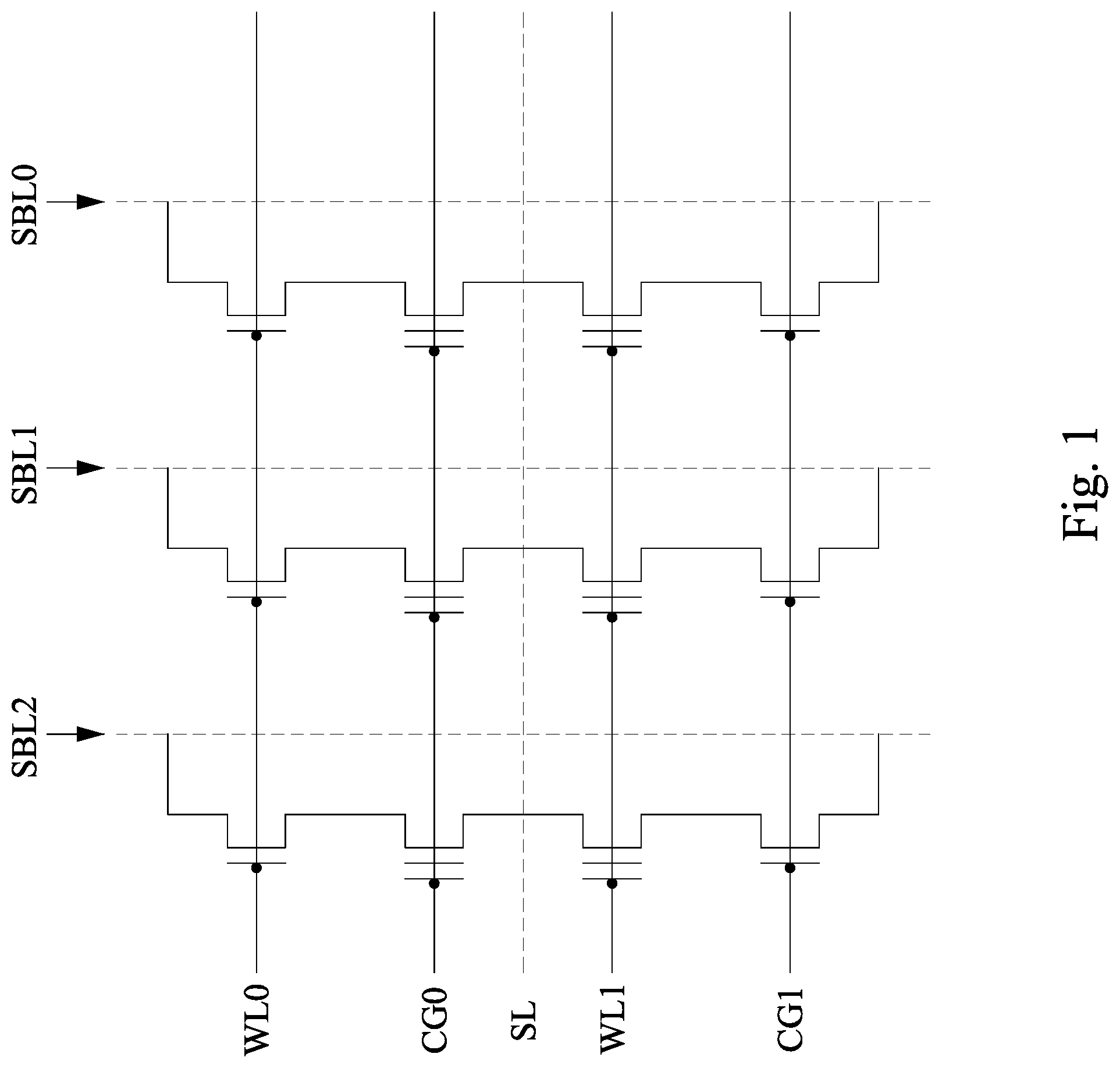
Reference is now made to . is a schematic diagram of a device, in accordance with various embodiments of the present disclosure.
As illustratively shown in , the device includes a plurality of memory cells. Gate terminals of the memory cells are coupled to a word line WL 0 , a word line WL 1 , a control gate line CG 0 , and a control gate line CG 1 respectively. The memory cells are coupled to each other in series to form a memory string, and there are plural of memory strings as shown in . A bit line signal SBL 0 , a bit line signal SBL 1 , and a bit line signal SBL 2 are input into one terminal of one of the memory strings respectively. In some embodiments, the memory strings are coupled to a source line SL, which will be described in the following description in detail.
The terms “comprise,” “comprising,” “include,” “including,” “has,” “having,” etc. used in this specification are open-ended and mean “comprises but not limited.” The terms used in this specification generally have their ordinary meanings in the art and in the specific context where each term is used. The use of examples in this specification, including examples of any terms discussed herein, is illustrative only, and in no way limits the scope and meaning of the disclosure or of any exemplified term. Likewise, the present disclosure is not limited to various embodiments given in this specification.
The above discussion merely describes exemplary connections that can be made in accordance with various alternative embodiments. It is understood that such various alternative embodiments are not limited to the specific connections described above or those shown in .
In some embodiments, the device in includes a flash memory. Flash memory can be formed on a bulk silicon substrate and uses various bias conditions to read and write data values. For example, an EFS 3 cell—or “third generation SUPERFLASH” cell—includes a pair of symmetric split gate memory cells, each of which includes a pair of source/drain regions with a channel region arranged there between. In the EFS 3 architecture, one of the source/drain regions for each of the split gate memory cells is a common source/drain region shared with its neighboring cell, while the other source/drain region is an individual source/drain unique to the cell. Within each split gate cell, a floating gate is arranged over the channel region of the cell, and a control gate is arranged over the floating gate. A select gate is arranged on one side of the floating and control gates (e.g., between an individual source/drain region of the EFS 3 cell and a sidewall of the floating and/or control gate). At least one memory cell is configured to store a variable charge level on its floating gate, wherein the level of this charge corresponds to a data state stored in the cell and is stored in a non-volatile manner so that the stored charge/data persists in the absence of power.
In some embodiments, flash memory cells can be electronically programmed and erased in memory arrays. Programming operation of these memory arrays includes charging a floating gate of a selected memory cell by applying suitable voltages to a select gate and a control gate of the selected memory cell. For example, a select gate decoder provides an on-signal to the select gate of the selected memory cell and off-signals to select gates of non-selected memory cells. In some cases, for saving chip spaces, a control gate decoder provides the same signal to the control gates of all memory cells. Since the control gates of the non-selected memory cells are provided with the same signal as that of the selected memory cell, the programming operation might be performed with undesired program disturb, which is the partial charging of the floating gates of non-selected memory cells. It is important that cells which are not selected for the programming cycle are not disturbed by the programming of the selected cell. In some cases, control gates of neighboring memory cells are controlled by different control gates.
Reference is now made to . is a lateral view of the device as shown in , in accordance with various embodiments of the present disclosure.
As illustratively shown in , the device also includes a plurality of memory cells, which are coupled to each other in series, such that a plurality of memory strings are formed. The gate terminals of the memory cells are also coupled to the word line WL 0 , the word line WL 1 , the control gate line CG 0 , and the control gate line CG 1 respectively. Compared with the device in , it is noted that the device in further includes a bit line BL 0 , a bit line BL 1 , and a bit line BL 2 . The bit line BL 0 , the bit line BL 1 , and the bit line BL 2 are coupled to one terminal of one of the memory strings respectively. The bit line BL 0 , the bit line BL 1 , and the bit line BL 2 transmit the bit line signal SBL 0 , the bit line signal SBL 1 , and the bit line signal SBL 2 to one terminal of one of the memory strings correspondingly.
In some embodiments, compared with the device in , it is noted that the device in further includes a contact portion C 1 , a contact portion C 2 , and a contact portion C 3 . As illustratively shown in , the contact portion C 1 , the contact portion C 2 , and the contact portion C 3 are coupled to one of the memory strings respectively. Furthermore, the contact portion C 1 , the contact portion C 2 , and the contact portion C 3 are coupled to the source line SL. In some embodiments, after the bit line BL 0 , the bit line BL 1 , and the bit line BL 2 transmit the bit line signal SBL 0 , the bit line signal SBL 1 , and the bit line signal SBL 2 into one terminal of one of the memory strings respectively, the bit line signal SBL 0 , the bit line signal SBL 1 , and the bit line signal SBL 2 flow from the memory strings to the contact portion C 1 , the contact portion C 2 , and the contact portion C 3 . For example, after the bit line BL 0 transmits the bit line signal SBL 0 into one terminal of the memory string, the bit line signal SBL 0 flows from the memory string to the contact portion C 1 . After the bit line BL 1 transmits the bit line signal SBL 1 into one terminal of the memory string, the bit line signal SBL 1 flows from the memory string to the contact portion C 2 . In addition, after the bit line BL 2 transmits the bit line signal SBL 2 into one terminal of the memory string, the bit line signal SBL 2 flows from the memory string to the contact portion C 3 .
Substantially, the bit line signal SBL 0 , the bit line signal SBL 1 , and the bit line signal SBL 2 flow from the contact portion C 1 , the contact portion C 2 , and the contact portion C 3 to the source line SL. Next, the bit line signal SBL 0 , the bit line signal SBL 1 , and the bit line signal SBL 2 flow from the source line SL to a source line driver (the source line driver will be shown in the following ).
In some cases, the device as shown in does not have the contact portion C 1 , the contact portion C 2 , and the contact portion C 3 . Accordingly, the bit line signal SBL 0 , the bit line signal SBL 1 , and the bit line signal SBL 2 cannot flow from the contact portion C 1 , the contact portion C 2 , and the contact portion C 3 to the source line SL. In such condition, the bit line signal SBL 0 , the bit line signal SBL 1 , and the bit line signal SBL 2 shall flow through the oxide diffusion as shown in to a common contact portion C 0 , and then the bit line signal SBL 0 , the bit line signal SBL 1 , and the bit line signal SBL 2 flow from the common contact portion C 0 to the source line SL. Since the resistance of the oxide diffusion is high and distances of the oxide diffusion, which the bit line signal SBL 0 , the bit line signal SBL 1 , and the bit line signal SBL 2 pass, are different, the bit line signal SBL 0 , the bit line signal SBL 1 , and the bit line signal SBL 2 perform different source line (SL) loadings. Specifically, if the bit line signal SBL 0 , the bit line signal SBL 1 , and the bit line signal SBL 2 want to converge on the contact portion C 0 , the bit line signal SBL 2 shall pass through a long distance in the oxide diffusion. In contrast to that, the bit line signal SBL 0 shall pass through a short distance in the oxide diffusion. Hence, the performance of the memory will be affected due to the different SL loadings.
As illustratively shown in , since each of the bit line signal SBL 0 , the bit line signal SBL 1 , and the bit line signal SBL 2 flows into the source line SL through one of the corresponding contact portions C 1 , C 2 , C 3 , the bit line signal SBL 0 , the bit line signal SBL 1 , and the bit line signal SBL 2 do not have to pass the transmit portion as shown in to converge on the source line SL, such that the source line loading to each of the bit line signal SBL 0 , the bit line signal SBL 1 , and the bit line signal SBL 2 are substantially the same. Specifically, the bit line signal SBL 0 flows into the source line SL through the contact portion C 1 , the bit line signal SBL 1 flows into the source line SL through the contact portion C 2 , and the bit line signal SBL 2 flows into the source line SL through the contact portion C 3 . Therefore, the bit line signal SBL 0 , the bit line signal SBL 1 , and the bit line signal SBL 2 do not have to pass the transmit portion as shown in to converge on the source line SL through the common contact portion C 0 . Since each of the bit line signal SBL 0 , the bit line signal SBL 1 , and the bit line signal SBL 2 flows from one of the bit line BL 0 , the bit line BL 1 , and the bit line BL 2 to the source line driver through one of the contact portion C 1 , the contact portion C 2 , and the contact portion C 3 and the source line SL, the resistances between the bit lines BL 0 , BL 1 , BL 2 and the source line driver are substantially the same. Hence, the source line loading to each of the bit line signal SBL 0 , the bit line signal SBL 1 , and the bit line signal SBL 2 are substantially the same.
The above discussion merely describes exemplary connections that can be made in accordance with various alternative embodiments. It is understood that such various alternative embodiments are not limited to the specific connections described above or those shown in .
Reference is now made to . is a structure diagram of the device as shown in and , in accordance with various embodiments of the present disclosure.
As illustratively shown in , it illustrates a top view of the device as shown in and . The device includes at least two transmit portions, for example, a transmit portion TP 1 , a transmit portion TP 2 . Furthermore, the device includes at least one contact portion, for example, a contact portion C 1 . The contact portion, for example, the contact portion C 1 , is couple to the transmit portion, for example, the transmit portion TP 1 .
Referring to both and , after the bit line BL 0 transmits the bit line signal SBL 0 into one terminal of the memory cell string, the bit line signal SBL 0 flows through the transmit portion TP 1 of the memory cell string to the contact portion C 1 . In other words, the transmit portion TP 1 of the memory cell string receives the bit line signal SBL 0 from the bit line BL 0 . Substantially, the contact portion C 1 transmits the bit line signal SBL 0 from the transmit portion TP 1 to the source line driver 500 through a metal layer ML 1 .
Reference is now made to both and . In some embodiments, the device includes at least two contact portions, for example, the contact portion C 1 , and the contact portion C 2 . One of the contact portions, for example, the contact portion C 1 , is coupled to one of the transmit portions, for example, the transmit portion TP 1 . Another one of the contact portions, for example, the contact portion C 2 , is coupled to another one of the transmit portions, for example, the transmit portion TP 2 . The contact portion C 1 and the contact portion C 2 are coupled to the metal layer ML 1 , and the metal layer ML 1 is coupled to the source line driver 500 .
In some embodiments, resistances between the at least two transmit portions and the source line driver are substantially the same. For example, the transmit portion TP 1 is coupled to the source line driver 500 through the contact portion C 1 and the metal layer ML 1 , and the transmit portion TP 2 is coupled to the source line driver 500 through the contact portion C 2 and the metal layer ML 1 . Therefore, the resistance between the transmit portion TP 1 and the source line driver 500 and the resistance between the transmit portion TP 2 and the source line driver 500 are substantially the same. It is noted that “the resistance between the transmit portion TP 1 and the source line driver 500 and the resistance between the transmit portion TP 2 and the source line driver 500 are substantially the same” means that the difference between the resistances is less than 20% of the greater/smaller resistance value.
Owing to resistances between the at least two transmit portions and the source line driver are substantially the same, the bit line BL 0 and the bit line BL 1 perform the same SL loading. Specifically, the bit line BL 0 and the bit line BL 1 input the bit line signal SBL 0 and the bit line signal SBL 1 to the transmit portion TP 1 and the transmit portion TP 2 , and the bit line signal SBL 0 and the bit line signal SBL 1 are transmitted to the source line driver 500 through the contact portion C 1 , the contact portion C 2 and the metal layer ML 1 . If the resistance between the transmit portion TP 1 and the source line driver 500 and the resistance between the transmit portion TP 2 and the source line driver 500 are substantially the same, the bit line BL 0 and the bit line BL 1 perform the same SL loading.
In some embodiments, one of the contact portions is coupled to one of the transmit portions in a one-on-one manner. For example, the contact portion C 1 is couple to the transmit portion TP 1 , the contact portion C 2 is couple to the transmit portion TP 2 , and the contact portion C 3 is couple to the transmit portion TP 3 .
In some embodiments, the transmit portions are disposed on the same layer. For example, the transmit portion T 1 , the transmit portion T 2 and the transmit portion T 3 are disposed on the same layer.
In some embodiments, the contact portions are disposed on a same layer. For example, the contact portion C 1 , the contact portion C 2 and the contact portion C 3 are disposed on the same layer.
The above discussion merely describes exemplary connections that can be made in accordance with various alternative embodiments. It is understood that such various alternative embodiments are not limited to the specific connections described above or those shown in .
Reference is now made to . is a structure diagram of the device as shown in and , in accordance with various embodiments of the present disclosure.
As illustratively shown in , it illustrates a top view of the device as shown in and . The device includes a plurality of transmit portions, for example, a transmit portion TP 1 , a transmit portion TP 2 , a transmit portion TP 3 . Furthermore, the device includes only one contact portion, for example, a contact portion C. The contact portion, for example, the contact portion C 1 , is couple to the transmit portions, for example, the transmit portion TP 1 , the transmit portion TP 2 , and the transmit portion TP 3 .
Referring to both , , after the bit line BL 0 , the bit line BL 1 and the bit line BL 2 transmit the bit line signal SBL 0 , the bit line signal SBL 1 and the bit line signal SBL 2 into one terminal of the memory cell strings respectively, the bit line signal SBL 0 , the bit line signal SBL 1 and the bit line signal SBL 2 flow through the transmit portion TP 1 , the transmit portion TP 2 and the transmit portion TP 3 to the contact portion C. In other words, the transmit portion TP 1 , the transmit portion TP 2 and the transmit portion TP 3 receive the bit line signal SBL 0 , the bit line signal SBL 1 and the bit line signal SBL 2 from the bit line BL 0 , the bit line BL 1 and the bit line BL 2 . Substantially, the contact portion C transmits the bit line signal SBL 0 , the bit line signal SBL 1 and the bit line signal SBL 2 from the transmit portion TP 1 , the transmit portion TP 2 and the transmit portion TP 3 to the source line driver 500 through the metal layer ML 1 .
In some embodiments, resistances between the plural transmit portions and the source line driver are substantially the same. For example, the transmit portion TP 1 is coupled to the source line driver 500 through the contact portion C and the metal layer ML 1 , the transmit portion TP 2 is coupled to the source line driver 500 through the contact portion C and the metal layer ML 1 , and the transmit portion TP 3 is coupled to the source line driver 500 through the contact portion C and the metal layer ML 1 . Therefore, the resistance between the transmit portion TP 1 and the source line driver 500 , the resistance between the transmit portion TP 2 and the source line driver 500 , and the resistance between the transmit portion TP 3 and the source line driver 500 are substantially the same. It is noted that “the resistances between the transmit portions TP 1 , TP 2 , TP 3 and the source line driver 500 are substantially the same” means that the difference between the resistances is less than 20% of the greater/smaller resistance value.
Owing to resistances between the plural transmit portions and the source line driver are substantially the same, the bit line BL 0 , the bit line BL 1 and the bit line BL 2 perform the same SL loading. Specifically, the bit line BL 0 , the bit line BL 1 and the bit line BL 2 input the bit line signal SBL 0 , the bit line signal SBL 1 and the bit line signal SBL 2 to the transmit portion TP 1 , the transmit portion TP 2 and the transmit portion TP 3 , and the bit line signal SBL 0 , the bit line signal SBL 1 and the bit line signal SBL 2 are transmitted to the source line driver 500 through the contact portion C and the metal layer ML 1 . If the resistances between the transmit portions TP 1 , TP 2 , TP 3 and the source line driver 500 are substantially the same, the bit line BL 0 , the bit line BL 1 and the bit line BL 2 perform the same SL loading.
The above discussion merely describes exemplary connections that can be made in accordance with various alternative embodiments. It is understood that such various alternative embodiments are not limited to the specific connections described above or those shown in .
is a schematic diagram of a device, in accordance with various embodiments of the present disclosure.
As illustratively shown in , a device includes a plurality of input/output (IO) buffers IO 0 , IO 1 , IO 2 , IO 3 . Each of the IO buffers IO 0 , IO 1 , IO 2 , IO 3 is coupled to four bit lines.
In some embodiments, the device can be a memory. When a read operation is performed to the device, the buffers IO 0 , IO 1 , IO 2 , IO 3 of the device can select one of the bit lines for reading. When a program operation is performed to the device, the bit lines will be programed sequentially.
Reference is now made to . is a flow diagram of a method for operating the device as shown in according to some embodiments of the present disclosure.
With reference to the method 600 in , in operation 610 , the memory cells of the device are erased to a low threshold. In some embodiments, after the memory cells of the device are erased, the SL bias is VS 1 .
In operation 620 , the memory cells are pre-programed to a first threshold during a pre-program period.
In some embodiments, reference is now made to the method 600 in together with the wave form in , which is a wave form diagram, in accordance with various embodiments of the present disclosure. As illustratively shown in , the memory cells are pre-programed to the first threshold during the pre-program period. After the memory cells of the device are pre-programed, the SL bias is VS 2 .
In operation 630 , the memory cells are programed to a second threshold during a program period.
In some embodiments, reference is now made to the method 600 in together with the wave form in , which is a wave form diagram, in accordance with various embodiments of the present disclosure. As illustratively shown in , the memory cells are programed to the second threshold during the program period. After the memory cells of the device are programed, the SL bias is VS 3 . In some embodiments, the second threshold is a program verify (PV) level.
In some embodiments, the first threshold and the second threshold are larger than the low threshold. In some embodiments, the second threshold is larger than the first threshold.
In some embodiments, a difference between the first threshold and the low threshold is larger than a difference between the second threshold and the first threshold. In some embodiments, the second threshold is near the first threshold.
During the program operation, when all the memory cells are programed to the target level, the SL bias for the IO buffer IO 0 will have a large offset, which will be described as follow. Firstly, when the memory cells corresponding to the IO buffer IO 0 are designed to a current I 1 , the SL bias for the IO buffer IO 0 is VS 2 . When all memory cells corresponding to the IO buffer IO 0 , IO 1 , IO 2 , IO 3 are designed to currents I 1 , I 2 , I 3 , I 4 respectively, the SL bias for the IO buffer IO 0 is VS 3 . In some cases, the VS 3 is much larger than VS 2 , and the offset of the SL bias for the IO buffer IO 0 is huge.
Therefore, the operation 620 is performed to pre-program all of the memory cells to a first threshold. Subsequently, the operation 630 is performed to program all of the memory cells to a second threshold. In such cases, the SL bias for the IO buffer IO 0 is VS 2 after pre-program operation, the SL bias for the IO buffer IO 0 is VS 3 after program operation, and difference of the VS 2 and the VS 3 is minor. Hence, the offset of the SL bias for the IO buffer IO 0 is reduced.
Also disclosed is a device. The device includes at least two transmit portions and at least one contact portion. Each of the at least two transmit portions is configured to receive a bit line signal. The at least one contact portion is couple to the at least two transmit portions respectively and configured to transmit the bit line signals from the least two transmit portions to a source line.
In some embodiments, the at least one contact portion comprises at least two contact portions, wherein one of the at least two contact portions is coupled to one of the at least two transmit portions, and another one of the at least two contact portions is coupled to another one of the at least two transmit portions.
In various embodiments, the source line is coupled to a source line driver.
In some embodiments, resistances between the at least two transmit portions and the source line driver are substantially the same.
In various embodiments, the at least two transmit portions comprise a first transmit portion and a second transmit portion. The first transmit portion is configured to receive a first bit line signal. The second transmit portion is configured to receive a second bit line signal.
In some embodiments, the at least two contact portions comprise a first contact portion and a second contact portion. The first contact portion is coupled to the first transmit portion and configured to transmit the first bit line signal from the first transmit portion to the source line. The second contact portion is coupled to the second transmit portion and configured to transmit the second bit line signal from the second transmit portion to the source line.
In various embodiments, a first resistance between the first transmit portion and the source line driver is substantially the same as a second resistance between the second transmit portion and the source line driver.
Also disclosed is a device that includes a plurality of transmit portions and a plurality of transmit portions. Each of the plurality of transmit portions is configured to receive a bit line signal. Each of the plurality of contact portions is coupled to one of the plurality of transmit portions, wherein the plurality of contact portions are configured to transmit the bit line signals from the plurality of transmit portions to a source line.
In some embodiments, one of the plurality of contact portions is coupled to one of the plurality of transmit portions in a one-on-one manner.
In various embodiments, the source line is coupled to a source line driver.
In some embodiments, resistances between the plurality of transmit portions and the source line driver are substantially the same.
In various embodiments, the plurality of transmit portions are disposed on a same layer.
In some embodiments, the plurality of contact portions are disposed on a same layer.
Also disclosed is a method that includes the operations below: erasing memory cells to a low threshold; pre-programing the memory cells to a first threshold during a pre-program period; and programing the memory cells to a second threshold during a program period.
In some embodiments, a difference between the first threshold and the low threshold is larger than a difference between the second threshold and the first threshold.
In some embodiments, the second threshold comprises a program verify.
In some embodiments, the first threshold is larger than the low threshold.
In some embodiments, the second threshold is larger than the low threshold.
In some embodiments, the second threshold is near the first threshold.
The foregoing outlines features of several embodiments so that those skilled in the art may better understand the aspects of the present disclosure. Those skilled in the art should appreciate that they may readily use the present disclosure as a basis for designing or modifying other processes and structures for carrying out the same purposes and/or achieving the same advantages of the embodiments introduced herein. Those skilled in the art should also realize that such equivalent constructions do not depart from the spirit and scope of the present disclosure, and that they may make various changes, substitutions, and alterations herein without departing from the spirit and scope of the present disclosure.
Figures (8)
Citations
This patent cites (10)
- US20040084716
- US20040084718
- US20060209585
- US20130051156
- US20130148409
- US20130343130
- US20140169105
- US20140198570
- US20150092494
- US20160329344