Display Device Capable of Displaying an Image of Uniform Brightness
Abstract
The present disclosure relates to a display device including first pixels disposed in a first pixel area, and connected to first scan lines; second pixels disposed in a second pixel area, and connected to second scan lines; a timing controller configured to supply a first clock signal and a second clock signal to a first clock line and a second clock line, respectively; a first scan driver configured to receive the first clock signal through the first clock line, and to supply a first scan signal to the first scan lines; and a second scan driver configured to receive the second clock signal through the second clock line, and to supply a second scan signal to the second scan lines, wherein the second pixel area has a smaller width than the first pixel area.
Claims (20)
1. A display device comprising: a first pixel area, a second pixel area disposed directly adjacent to one edge of the first pixel area, a third pixel area disposed on the one edge of the first pixel area with the second pixel area disposed between the first pixel area and the third pixel area, a fourth pixel area disposed directly adjacent to the one edge of the first pixel area and spaced apart from the second pixel area, and a fifth pixel area disposed on the one edge of the first pixel area with the fourth pixel area disposed between the first pixel area and the fifth pixel area; first pixels disposed in the first pixel area and electrically connected to first scan lines; second pixels disposed in the second pixel area and electrically connected to second scan lines; third pixels disposed in the third pixel area and electrically connected to third scan lines; fourth pixels disposed in the fourth pixel area and electrically connected to fourth scan lines; fifth pixels disposed in the fifth pixel area and electrically connected to fifth scan lines; a timing controller supplying a first clock signal, a second clock signal, a third clock signal, a fourth clock signal, and a fifth clock signal to a first clock line, a second clock line, a third clock line, a fourth clock line, and a fifth clock line, respectively; a first scan driver generating a first scan signal using the first clock signal, and supplying the first scan signal to the first scan lines; a second scan driver generating a second scan signal using the second clock signal and supplying the second scan signal to the second scan lines; a third scan driver generating a third scan signal using the third clock signal and supplying the third scan signal to the third scan lines, a fourth scan driver generating a fourth scan signal using the fourth clock signal and supplying the fourth scan signal to the fourth scan lines; and a fifth scan driver generating a fifth scan signal using the fifth clock signal and supplying the fifth scan signal to the fifth scan lines, wherein the first pixel area, the second pixel area, and the third pixel area have widths different from one another, and wherein the first clock signal, the second clock signal, and the third clock signal have signal characteristics different from one another.
Show 19 dependent claims
2. The display device according to claim 1 , wherein the signal characteristics comprise at least one of a pulse width, a length of a rising edge period and a length of a falling edge period.
3. The display device according to claim 2 , wherein the pulse width of the second clock signal is set to be smaller than the pulse width of the first clock signal.
4. The display device according to claim 3 , wherein the pulse width of the third clock signal is set to be smaller than the pulse width of the second clock signal.
5. The display device according to claim 3 , wherein the rising edge period of the third clock signal is set to be longer than the rising edge period of the first clock signal.
6. The display device according to claim 5 , wherein the third clock signal has a staircase wave form, and wherein the third clock signal changes from a low voltage to a high voltage via an intermediate voltage during the rising edge period.
7. The display device according to claim 3 , wherein the falling edge period of the third clock signal is set to be longer than the falling edge period of the first clock signal.
8. The display device according to claim 7 , wherein the third clock signal has a staircase wave form, and wherein the third clock signal changes from a high voltage to a low voltage via an intermediate voltage during the falling edge period.
9. The display device according to claim 2 , wherein the rising edge period of the second clock signal is set to be longer than the rising edge period of the first clock signal.
10. The display device according to claim 9 , wherein the rising edge period of the third clock signal is set to be longer than the rising edge period of the second clock signal.
11. The display device according to claim 9 , wherein the pulse width of the third clock signal is set to be smaller than the pulse width of the first clock signal.
12. The display device according to claim 11 , further comprising: a substrate in which the first to fifth pixel areas are defined, the substrate including a concave part from which a portion of the substrate is removed, wherein the second pixel area and the third pixel area are spaced apart from the fourth pixel area and the fifth pixel area, respectively, with the concave part of the substrate disposed therebetween.
13. The display device according to claim 2 , wherein the falling edge period of the second clock signal is set to be longer than the falling edge period of the first clock signal.
14. The display device according to claim 13 , wherein the falling edge period of the third clock signal is set to be longer than the falling edge period of the second clock signal.
15. The display device according to claim 14 , wherein the pulse width of the third clock signal is set to be smaller than the pulse width of the first clock signal.
16. The display device according to claim 1 , wherein lengths of the second scan lines in the second pixel area are shorter than lengths of the first scan lines in the first pixel area, and wherein lengths of the third scan lines in the third pixel area are shorter than lengths of the second scan lines in the second pixel area.
17. The display device according to claim 1 , wherein a number of the second pixels is smaller than a number of the first pixels, and wherein a number of the third pixels is smaller than the number of the second pixels.
18. The display device according to claim 1 , wherein the fourth pixel area and the fifth pixel area have widths different from each other, and wherein the fourth clock signal and the fifth clock signal have signal characteristics different from each other.
19. The display device according to claim 18 , wherein the fourth clock signal has the signal characteristic different from the signal characteristic of the second clock signal.
20. The display device according to claim 18 , wherein the fifth clock signal has the signal characteristic different from the signal characteristic of the third clock signal.
Full Description
Show full text →
CROSS-REFERENCE TO RELATED APPLICATION
This application is a continuation-in-part of U.S. patent application Ser. No. 17/335,032 filed on May 31, 2021, which is a continuation application of U.S. patent application Ser. No. 15/587,192 filed on May 4, 2017, which claims priority under 35 USC § 119 to Korea Patent Application No. 10-2016-0068361, filed on Jun. 1, 2016, in the Korean Intellectual Property office, the entire contents of which are incorporated herein by reference in their entirety.
BACKGROUND
1. Field
Embodiments of the present disclosure relate to a display device.
2. Description of Related Art
With the development of the informatization technology, the importance of a display device that is a medium connecting users and information is being emphasized. Recently, liquid crystal display devices, organic light emitting display devices and the like are widely being used.
Such display devices may include a plurality of pixels for displaying images, the pixels may be connected to driving wires.
Here, loads of the driving wires may differ depending on the locations of the driving wires.
SUMMARY
A purpose of the present disclosure is to resolve the aforementioned problem, that is, to provide a display device capable of displaying an image of uniform brightness.
According to an embodiment of the present disclosure, there is provided a display device including first pixels disposed in a first pixel area, and connected to first scan lines; second pixels disposed in a second pixel area, and connected to second scan lines; a timing controller configured to supply a first clock signal and a second clock signal to a first clock line and a second clock line, respectively; a first scan driver configured to receive the first clock signal through the first clock line, and to supply a first scan signal to the first scan lines; and a second scan driver configured to receive the second clock signal through the second clock line, and to supply a second scan signal to the second scan lines, wherein the second pixel area has a smaller width than the first pixel area.
Further, the first clock signal and the second clock signal may have a different signal characteristic.
Further, the signal characteristic may include at least one of a pulse width, a length of a rising edge period and a length of a falling edge period.
Further, the pulse width of the second clock signal may be set to be smaller than the pulse width of the first clock signal.
Further, the rising edge period of the second clock signal may be set to be longer than the rising edge period of the first clock signal.
Further, the second clock signal may have a staircase wave form and the second clock signal may change from a low voltage to a high voltage via an intermediate voltage during the rising edge period.
Further, the falling edge period of the second clock signal may be set to be longer than the falling edge period of the first clock signal.
Further, the second clock signal may have a staircase wave form and the second clock signal may change from a high voltage to a low voltage via an intermediate voltage during the falling edge period.
Further, the second pixel area may have a shorter length than the first pixel area.
Further, lengths of the second scan lines may be shorter than lengths of the first scan lines.
Further, the number of the second pixels may be smaller than the number of the first pixels.
Further, the display device may further include third pixels disposed in a third pixel area having a smaller width than the first pixel area, and connected to third scan lines; and a third scan driver configured to receive a third clock signal through a third clock line, and to supply a third scan signal to the third scan lines.
Further, the timing controller may further supply the third clock signal to the third clock line.
Further, the first clock signal and the third clock signal may have a different signal characteristic.
Further, the signal characteristic may include at least one of a pulse width, a length of a rising edge period and a length of a falling edge period.
Further, the pulse width of the third clock signal may be set to be smaller than the pulse width of the first clock signal.
Further, the rising edge period of the third clock signal may be set to be longer than the rising edge period of the first clock signal.
Further, the third clock signal has a staircase wave form and the third clock signal may change from a low voltage to a high voltage via an intermediate voltage during the rising edge period.
Further, the falling edge period of the third clock signal may be set to be longer than the falling edge period of the first clock signal.
Further, the third clock signal has a staircase wave form and third clock signal may change from a high voltage to a low voltage via an intermediate voltage during the falling edge period.
Further, the third pixel area may have a shorter length than the first pixel area.
Further, lengths of the third scan lines may be shorter than lengths of the first scan lines.
Further, the number of the third pixels may be smaller than the number of the first pixels.
Further, the second pixel area may be disposed between the first pixel area and the third pixel area.
Further, the third pixel area may be spaced apart from the second pixel area.
According to another embodiment of the present disclosure, there is provided a display device including first pixels disposed in a first pixel area, and connected to first scan lines; second pixels disposed in a second pixel area, and connected to second scan lines; third pixels disposed in a third pixel area, and connected to third scan lines; a timing controller configured to supply a first clock signal, a second clock signal, and a third clock signal to a first clock line, a second clock line, and a third clock line, respectively; a first scan driver configured to generate a first scan signal using the first clock signal, and to supply the first scan signal to the first scan lines; a second scan driver configured to generate a second scan signal using the second clock signal, and to supply the second scan signal to the second scan lines; and a third scan driver configured to generate a third scan signal using the third clock signal, and to supply the third scan signal to the third scan lines, wherein the first pixel area, the second pixel area, and the third pixel area has a width different from one another.
Further, the first clock signal, the second clock signal, and the third clock signal may have a signal characteristic different from one another.
Further, the signal characteristic may include at least one of a pulse width, a length of a rising edge period and a length of a falling edge period.
According to another embodiment of the present disclosure, there is provided a display device including a display panel including a first display area having a first gate line to which a first number of pixels are connected and a second display area having a second gate line to which a second number of pixels are connected, the second number being smaller than the first number; and a controller providing a first scan control signal and a second scan control signal to a first scan driver connected to the first gate line and a second scan driver connected to the second gate line, respectively, wherein the first scan driver and the second scan driver provide a first clock signal and the second clock signal to the first scan line and the second scan line, respectively, and wherein the first clock signal and the second clock signal have a different signal characteristic.
Further, the different signal characteristic may include at least one of a pulse width, a length of a rising edge period and a length of a falling edge period.
Further, the pulse width of the first clock signal may be greater than that of the second clock signal.
The length of the rising edge period of the second clock signal may be greater than that of the first clock signal.
The length of the falling edge period of the second clock signal may be greater than that of the first clock signal.
According to the present disclosure as mentioned above, it is possible to provide a display device capable of displaying an image of uniform brightness by reducing a difference of brightness occurring between a plurality of pixel areas.
BRIEF DESCRIPTION OF THE DRAWINGS
Example embodiments will now be described more fully hereinafter with reference to the accompanying drawings; however, they may be embodied in different forms and should not be construed as limited to the embodiments set forth herein. Rather, these embodiments are provided so that this disclosure will be thorough and complete, and will fully convey the scope of the example embodiments to those skilled in the art.
In the drawing figures, dimensions may be exaggerated for clarity of illustration. It will be understood that when an element is referred to as being “between” two elements, it can be the only element between the two elements, or one or more intervening elements may also be present between the two elements. Like reference numerals refer to like elements throughout.
A and B are views each illustrating a pixel area of a display device according to an embodiment of the present disclosure;
is a view illustrating a display device according to an embodiment of the present disclosure;
is a view illustrating in further detail of a display driver illustrated in ;
is a view illustrating in further detail of a first scan driver and a second scan driver illustrated in ;
is a waveform view illustrating a first to fourth clock signals and a first and second scan signals according to the embodiment of the present disclosure;
is a waveform view illustrating the third and fourth clock signals and the second scan signal according to the embodiment of the present disclosure;
is a waveform view illustrating the third and fourth clock signals and the second scan signal according to another embodiment of the present disclosure;
is a view illustrating an embodiment of a scan stage circuit illustrated in ;
is a view illustrating an embodiment of a first pixel illustrated in ;
is a view illustrating the display device according to the embodiment of the present disclosure;
is a view illustrating in further detail of the display driver illustrated in ;
is a view illustrating in further detail of the first to third scan drivers illustrated in ;
is a waveform view illustrating a fifth and sixth clock signals and a third scan signal according to the embodiment of the present disclosure;
is a waveform view illustrating the fifth and sixth clock signals and the third scan signal according to another embodiment of the present disclosure;
is a view illustrating the display device according to the embodiment of the present disclosure;
is a view illustrating in further detail of the display driver illustrated in ;
is a view illustrating in further detail of the first to third drivers illustrated in ;
is a view illustrating the display device according to the embodiment of the present disclosure;
is a view illustrating in further detail of the display driver illustrated in ;
is a view illustrating in further detail of the first to fifth scan drivers illustrated in ;
is a waveform view illustrating seventh to tenth clock signals and fourth and fifth scan signals according to the embodiment of the present disclosure;
is a waveform view illustrating the tenth clock signals and the fourth and fifth scan signals according to another embodiment of the present disclosure;
is a view illustrating in further detail of the display driver illustrated in ; and
is a view illustrating in further detail of the first to fifth scan drivers illustrated in .
DETAILED DESCRIPTION
Specific matters of other embodiments are included in the detailed description and the drawings.
Hereinafter, embodiments will be described in greater detail with reference to the accompanying drawings. Embodiments are described herein with reference to cross-sectional illustrations that are schematic illustrations of embodiments (and intermediate structures). As such, variations from the shapes of the illustrations as a result, for example, of manufacturing techniques and/or tolerances, are to be expected. Thus, embodiments should not be construed as limited to the particular shapes of regions illustrated herein but may include deviations in shapes that result, for example, from manufacturing. In the drawings, lengths and sizes of layers and regions may be exaggerated for clarity. Like reference numerals in the drawings denote like elements. It is also noted that in this specification, “connected/coupled” refers to one component not only directly coupling another component but also indirectly coupling another component through an intermediate component. On the other hand, “directly connected/directly coupled” refers to one component directly coupling another component without an intermediate component.
Hereinafter, a display device according to an embodiment of the present disclosure will be explained with reference to the drawings related to the embodiments of the present disclosure.
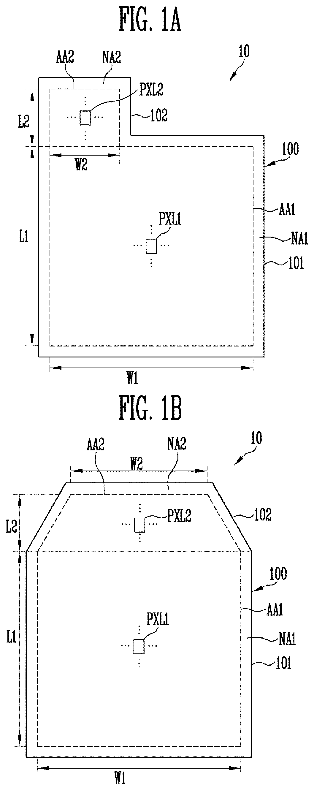
A and B are views each illustrating a pixel area of the display device according to an embodiment of the present disclosure.
Referring to A , the display device 10 according to the embodiment of the present disclosure may include pixel areas AA 1 , AA 2 and peripheral areas NA 1 , NA 2 .
In the pixel areas AA 1 , AA 2 , a plurality of pixels PXL 1 , PXL 2 are disposed, and accordingly, a certain image may be displayed on the pixel areas AA 1 , AA 2 . Therefore, the pixel areas AA 1 , AA 2 may be called display areas.
In the peripheral areas NA 1 , NA 2 , elements for driving the pixels PXL 1 , PXL 2 (for example, driver and wire, etc.) may be disposed. Since there are no pixels PXL 1 , PXL 2 in the peripheral areas NA 1 , NA 2 , the peripheral areas NA 1 , NA 2 may be called as non-display areas.
For example, the peripheral areas NA 1 , NA 2 may exist outside the pixel areas AA 1 , AA 2 , and may surround at least a portion of the pixel areas AA 1 , AA 2 .
The pixel areas AA 1 , AA 2 may include a first pixel area AA 1 , and a second pixel area AA 2 .
The second pixel area AA 2 may be disposed at one side of the first pixel area AA 1 , and may have a smaller surface area than the first pixel area AA 1 .
For example, a width W 2 of the second pixel area AA 2 may be set to be smaller than a width W 1 of the first pixel area AA 1 , and a length L 2 of the second pixel area AA 2 may be set to be shorter than a length L 1 of the first pixel area AA 1 .
The peripheral areas NA 1 , NA 2 may include a first peripheral area NA 1 and a second peripheral area NA 2 .
The first peripheral area NA 1 may exist on a periphery of the first pixel area AA 1 , and may surround at least a portion of the first pixel area AA 1 .
A width of the first peripheral area NA 1 may be set to be the same overall. However, there is no limitation thereto, and thus the width of the first peripheral area NA 1 may be set to differ depending on the location of the first peripheral area NA 1 .
The second peripheral area NA 2 may exist on a periphery of the second pixel area AA 2 , and may surround at least a portion of the second pixel area AA 2 .
A width of the second peripheral area NA 2 may be set to be the same overall. However, there is no limitation thereto, and thus the width of the second peripheral area NA 2 may be set to differ depending on the location of the second peripheral area NA 2 .
The pixels PXL 1 , PXL 2 may include first pixels PXL 1 and second pixels PXL 2 .
For example, the first pixels PXL 1 may be disposed in the first pixel area AA 1 , and the second pixels PXL 2 may be disposed in the second pixel area AA 2 .
The pixels PXL 1 , PXL 2 may emit light of a predetermined brightness according to a control by a driver, and for this purpose, the pixels PXL 1 , PXL 2 may include a light emitting element (for example, organic light emitting diode).
The pixel areas AA 1 , AA 2 and the peripheral areas NA 1 , NA 2 may be disposed on a substrate 100 of the display device 10 .
The substrate 100 may be formed in various shapes such that the pixel areas AA 1 , AA 2 and the peripheral areas NA 1 , NA 2 may be formed thereon.
For example, the substrate 100 may include a plate type base substrate 101 , and a subsidiary substrate 102 that protruded from one end of the base substrate 101 .
Here, the subsidiary substrate 102 may have a smaller surface area than the base substrate 101 . For example, a width of the subsidiary substrate 102 may be set to be smaller than a width of the base substrate 101 , and a length of the subsidiary substrate 102 may be set to be shorter than a length of the base substrate 101 .
The subsidiary substrate 102 may have the same or similar shape as the second pixel area AA 2 , but without limitation, and thus may have a shape different from the second pixel area AA 2 .
The substrate 100 may be made of an insulating material such as glass and resin, etc. Further, the substrate 100 may be made of a material having flexibility such that it may be bent or curved, and may have a single-layered or multi-layered structure.
For example, the substrate 100 may include at least one of polystyrene, polyvinyl alcohol, polymethyl methacrylate, polyethersulfone, polyacrylate, polyetherimide, polyethylene naphthalate, polyethylene terephthalate, polyphenylene sulfide, polyarylate, polyimide, polycarbonate, triacetate cellulose, and cellulose acetate propionate.
However, the substrate 100 may be made of various other materials as well, for example, fiber glass reinforced plastic (FRP) and the like.
The second pixel area AA 2 may have various shapes. For example, the second pixel area AA 2 may have a polygonal shape, circular shape and the like. Further, at least a portion of the second pixel area AA 2 may have a curve shape.
For example, the second pixel area AA 2 may have a rectangular shape as illustrated in A .
Further, referring to B , the second pixel area AA 2 may have a trapezoid shape where a long parallel side of the trapezoid are connected to the first pixel area AA 1 .
In accordance with the change of shape of the second pixel area AA 2 , the number of the second pixels PXL 2 disposed in one row may differ depending on its location.
In the case of the second pixel area AA 2 illustrated in B , the number of the second pixels PXL 2 disposed in the one row may vary depend on the location in the second pixel area AA 2 . For example, the closer the one row is to the first pixel area AA 1 , the more second pixels PXL 2 may be disposed in the one row.
is a view illustrating a display device according to an embodiment of the present disclosure. The display device 10 illustrated in is based on the pixel areas AA 1 , AA 2 illustrated in A , but it may be applied to pixel areas AA 1 , AA 2 having different shapes as those illustrated in B .
Referring to , the display device 10 according to the embodiment of the present disclosure may include first pixels PXL 1 , second pixels PXL 2 , and a display driver 200 .
The first pixels PXL 1 may be disposed in the first pixel area AA 1 . Each of the first pixels PXL 1 may be connected to a first scan line S 1 , a first emission control line E 1 , and a first data line D 1 , respectively.
The second pixels PXL 2 may be disposed in the second pixel area AA 2 . Each of the second pixels PXL 2 may be connected to a respective second scan line S 2 , a second emission control line E 2 , and a second data line D 2 , respectively.
When necessary, the pixels PXL 1 , PXL 2 may be connected to a plurality of scan lines.
The display driver 200 may control the emission of the pixels PXL 1 , PXL 2 by supplying driving signals to the pixels PXL 1 , PXL 2 .
For example, the display driver 200 may supply a scan signal to the pixels PXL 1 , PXL 2 through the scan lines S 1 , S 2 , supply a emission control signal to the pixels PXL 1 , PXL 2 through the emission control lines E 1 , E 2 , and supply a data signal to the pixels PXL 1 , PXL 2 through the data lines D 1 , D 2 .
An entirety or a portion of the display driver 200 may be formed directly onto the substrate 100 , or connected to the substrate 100 via a separate constituent element 110 such as a flexible printed circuit board or the like.
For example, the display driver 200 may be installed by various methods such as the Chip on Glass, Chip on Plastic, Tape Carrier Package and Chip on Film, etc.
Meanwhile, although it is illustrated in that the display driver 200 formed separately from the substrate 100 is installed on the substrate 100 , there is no limitation thereto.
For example, an entirety or a portion of the display driver 200 may be formed directly on the substrate, in which case it may be disposed in the first peripheral area NA 1 and the second peripheral area NA 2 of the substrate 100 .
is a view illustrating in further detail of the display driver illustrated in .
Referring to , the display driver 200 according to an embodiment of the present disclosure may include a first scan driver 210 , a second scan driver 220 , a data driver 260 , a timing controller 270 , a first emission driver 310 , and a second emission driver 320 .
The first scan driver 210 may supply a first scan signal to the first pixels PXL 1 through first scan lines S 11 ˜S 1 k.
For example, the first scan driver 210 may sequentially supply the first scan signal to the first scan lines S 11 ˜S 1 k.
In the case where the first scan driver 210 is formed directly on the substrate 100 , the first scan driver 210 may be disposed in the first peripheral area NA 1 .
The second scan driver 220 may supply a second scan signal to the second pixels PXL 2 through second scan lines S 21 ˜S 2 j.
For example, the second scan driver 220 may sequentially supply the second scan signal to the second scan lines S 21 ˜S 2 j.
In the case where the second scan driver 220 is formed directly on the substrate 100 , the second scan driver 220 may be disposed in the second peripheral area NA 2 .
The scan signal may be set to a gate on voltage (for example, low voltage) so that a transistor included in the pixels PXL 1 , PXL 2 may be turned on.
The first scan driver 210 and the second driver 220 may operate in response to a first scan control signal SCS 1 and a second scan control signal SCS 2 , respectively.
The data driver 260 may supply a data signal to the first pixels PXL 1 through first data lines D 11 ˜D 1 o.
The first pixels PXL 1 may be connected to a first pixel power source ELVDD and a second pixel power source ELVSS. When necessary, the first pixels PXL 1 may be additionally connected to an initialization power source Vint.
Such first pixels PXL 1 may be supplied with the data signal through the first data lines D 11 ˜D 10 when the first scan signal is supplied to the first scan lines S 11 ˜S 1 k , and the first pixels PXL 1 supplied with the data signal may control the amount of current flowing from the first pixel power source ELVDD to the second pixel power source ELVSS via an organic light emitting diode (not illustrated).
Further, the number of first pixels PXL 1 disposed in one row may differ depending on its location.
The data driver 260 may supply data signals to the second pixels PXL 2 through second data lines D 21 ˜D 2 p.
For example, the second data lines D 21 ˜D 2 p may be connected to some of the first data lines D 11 ˜D 1 m −1.
Further, the second pixels PXL 2 may be connected to the first pixel power source ELVDD and the second pixel power source ELVSS. When necessary, the second pixels PXL 2 may be additionally connected to the initialization power source Vint.
Such second pixels PXL 2 may be supplied with the data signal from the second data lines D 21 ˜D 2 p when the second scan signal is supplied to the second scan lines S 21 ˜S 2 j , and the second pixels PXL 2 supplied with the data signal may control the amount of current flowing from the first pixel power source ELVDD to the second pixel power source ELVSS via the organic light emitting diode (not illustrated).
Further, the number of second pixels PXL 2 disposed in one row may differ depending on its location.
Here, the data driver 260 may operate in response to a data control signal DCS.
The first emission driver 310 may supply a first emission control signal to the first pixels PXL 1 through first emission control lines E 11 ˜E 1 k.
For example, the first emission driver 310 may sequentially supply the first emission control signal to the first emission control lines E 11 ˜E 1 k.
In the case where the first emission driver 310 is formed directly on the substrate 100 , the first emission driver 310 may be disposed in the first peripheral area NA 1 .
In the case when the first pixels PXL 1 need not use the first emission control signal, the first emission driver 310 and the first emission control lines E 11 ˜E 1 k may be omitted.
The second emission driver 320 may supply a second emission control signal to the second pixels PXL 2 through second emission control lines E 21 ˜E 2 j.
For example, the second emission driver 320 may sequentially supply the second emission control signal to the second emission control lines E 21 ˜E 2 j.
In the case where the second emission driver 320 is formed directly on the substrate 100 , the second emission driver 320 may be disposed in the second peripheral area NA 2 .
In the case when the second pixels PXL 2 need not use the second emission control signal, the second emission driver 320 and the second emission control lines E 21 ˜E 2 j may be omitted.
The emission control signal is used to control the light emission time of the pixels PXL 1 , PXL 2 . For this purpose, the emission control signal may be set to have a wider width than the scan signal.
For example, the emission control signal may be set to a gate off voltage (for example, high voltage) so that the transistor included in the pixels PXL 1 , PXL 2 may be turned off.
The first emission driver 310 and the second emission driver 320 may operate in response to the first emission control signal ECS 1 and the second emission control signal ECS 2 , respectively.
Since the second pixel area AA 2 has a smaller surface area than the first pixel area AA 1 , the number of the second pixels PXL 2 may be smaller than the number of the first pixels PXL 1 , and the lengths of the second scan lines S 21 ˜S 2 j and the second emission control lines E 21 ˜E 2 j may be shorter than the first scan lines S 11 ˜S 1 k and the first emission control lines E 11 ˜E 1 k.
The number of second pixels PXL 2 connected to any one of the second scan lines S 21 ˜S 2 j may be smaller than the number of the first pixels PXL 1 connected to any one of the first scan lines S 11 ˜S 1 k.
Further, the number of the second pixels PXL 2 connected to any one of the second emission control lines E 21 ˜E 2 j may be smaller than the number of the first pixels PXL 1 connected to any one of the first emission control lines E 11 ˜E 1 k.
The timing controller 270 may control the first scan driver 210 , the second scan driver 220 , the data driver 260 , the first emission driver 310 , and the second emission driver 320 .
For this purpose, the timing controller 270 may supply the first scan control signal SCS 1 and the second scan control signal SCS 2 to the first scan driver 210 and the second scan driver 220 , respectively, and supply the first emission control signal ECS 1 and the second emission control signal ECS 2 to the first emission driver 310 and the second emission driver 320 , respectively.
Here, each of the scan control signals SCS 1 , SCS 2 and the emission control signals ECS 1 , ECS 2 may include at least one clock signal and a start pulse.
The start pulse may control the timing of the first scan signal or the first emission control signal. The clock signal may be used to shift the start pulse.
Further, the timing controller 270 may supply a data control signal DCS to the data driver 260 .
In the data control signal DCS, a source start pulse and at least one clock signal may be included. The source start pulse may control a sampling starting time point of the data, and the clock signal may be used to control a sampling operation.
Meanwhile, loads of the first scan lines S 11 ˜S 1 k and loads of the second scan lines S 21 ˜S 2 j may be different from each other.
That is, since the lengths of the first scan lines S 11 ˜S 1 k are longer than the second scan lines S 21 ˜S 2 j , and the number of the first pixels PXL 1 connected to a same first scan line is greater than the number of the second pixels PXL 2 connected to a same scan line, the loads of the first scan lines S 11 ˜S 1 k may be greater than the second scan lines S 21 ˜S 2 j.
This causes a difference of time constant between the first scan signal and the second scan signal, and eventually, a greater RC delay occurs in the first scan signal than the second scan signal.
Accordingly, the data entry time regarding the first pixels PXL 1 becomes shorter than that of the second pixels PXL 2 , and consequently, a difference of brightness occurs between the first pixels PXL 1 and the second pixels PXL 2 .
Therefore, in the embodiment of the present disclosure, a clock line is separately installed for each of the first scan driver 210 and the second scan driver 220 , and the characteristics of the clock signals being supplied to each clock line are adjusted to be different from each other, thereby setting the data entry time of the first pixels PXL 1 and the data entry time of the second pixels PXL 2 to be similar to each other.
Accordingly, the difference of brightness between the first pixel area AA 1 and the second pixel area AA 2 may be reduced.
Hereinafter, the configuration of the present disclosure related to the aforementioned will be explained in further detail.
is a view illustrating in further detail of the first scan driver and the second scan driver illustrated in .
Referring to , a first clock line 241 and a second clock line 242 may be connected between the timing controller 270 and the first scan driver 210 , and a third clock line 243 and a fourth clock line 244 may be connected between the timing controller 270 and the second scan driver 220 .
The first and second clock lines 241 , 242 associated with the first scan driver 210 and the third and fourth clock lines 243 , 244 associated with the second scan driver 220 may be disposed such that they are not electrically connected to each other.
The first clock line 241 and the second clock line 242 may respectively transmit a first clock signal CLK 1 and a second clock signal CLK 2 being supplied from the timing controller 270 to the first scan driver 210 , and the third clock line 243 and the fourth clock line 244 may respectively supply a third clock signal CLK 3 and a fourth clock signal CLK 4 being supplied from the timing controller 270 to the second scan driver 220 .
In the case where the clock lines are not electrically connected as mentioned above, some of the loads of the first scan lines S 11 ˜S 1 k become smaller than when the first scan driver 210 and the second scan driver 220 share the same clock line, thereby reducing some of the RC delay of the first scan signal.
The first clock signal CLK 1 and the second clock signal CLK 2 may have different phases. For example, the second clock signal CLK 2 may have a phase difference of 180° compared to the first clock signal CLK 1 . That is, the second clock signal CLK 2 may be an inverted clock signal of the first clock signal CLK 1 .
The third clock signal CLK 3 and the fourth clock signal CLK 4 may have different phases. For example, the third clock signal CLK 3 may have a phase difference of 180° compared to the fourth clock signal CLK 4 . That is, the fourth clock signal CLK 4 may be an inverted clock signal of the third clock signal CLK 3 .
The first scan driver 210 may include a plurality of scan stage circuits SST 11 ˜SST 1 k.
Each of the scan stage circuits SST 11 ˜SST 1 k of the first scan driver 210 may be connected to one end of the first scan lines S 11 ˜S 1 k , and may each supply a first scan signal to the first scan lines S 11 ˜S 1 k.
Here, the scan stage circuits SST 11 ˜SST 1 k may operate in response to the clock signals CLK 1 , CLK 2 being supplied from the timing controller 270 . Further, the scan stage circuits SST 11 ˜SST 1 k may have the same configuration.
The scan stage circuits SST 11 ˜SST 1 k may be supplied with an output signal (that is, scan signal) of a previous scan stage circuit or a start pulse SSP 1 .
For example, the first scan stage circuit SST 11 may be supplied with the start pulse SSP 1 , and the rest of the scan stage circuits SST 12 ˜SST 1 k may be supplied with the output signal of the previous stage circuit.
In another embodiment, the first scan stage circuit SST 11 of the first scan driver 210 may use a signal being output from the last scan stage circuit SST 2 j of the second scan driver 220 as the start pulse.
Each of the scan stage circuits SST 11 ˜SST 1 k may be supplied with a first driving power source VDD 1 and a second driving power source VSS 1 .
Here, the first driving power source VDD 1 may be set to a gate off voltage, for example, a high level voltage. Further, the second driving power source VSS 1 may be set to a gate on voltage, for example, a low level voltage.
The second scan driver 220 may include a plurality of scan stage circuits SST 21 ˜SST 2 j.
Each of the scan stage circuits SST 21 ˜SST 2 j of the second scan driver 220 may be connected to one end of the second scan lines S 21 ˜S 2 j , and may supply a second scan signal to the second scan lines S 21 ˜S 2 j.
Here, the scan stage circuits SST 21 ˜SST 2 j may operate in response to the clock signals CLK 3 , CLK 4 being supplied from the timing controller 270 . Further, the scan stage circuits SST 21 ˜SST 2 j may have the same configuration.
The scan stage circuits SST 21 ˜SST 2 j may be supplied with an output signal (that is, scan signal) of a previous scan stage circuit or a start pulse SSP 2 .
For example, the first scan stage circuit SST 21 may be supplied with the start pulse SSP 2 , and the rest of the scan stage circuits SST 22 ˜SST 2 j may be supplied with the output signal of the previous scan stage circuit.
Further, the last scan stage circuit SST 2 j of the second driver 220 may supply an output signal to the first scan stage circuit SST 11 of the first scan driver 210 .
Each of the scan stage circuits SST 21 ˜SST 2 j may be supplied with the first driving power source VDD 1 and the second driver power source VSS 1 .
In , it is illustrated that the scan drivers 210 , 220 each use two clock signals, but the number of the clock signals that the scan drivers 210 , 220 use may differ depending on the structure of the scan stage circuit.
is a waveform view of the first to fourth clock signals and the first and second scan signals according to an embodiment of the present disclosure. In , only the first scan signals being supplied to the first scan line S 11 and the second first scan line S 12 , and the second scan signals being supplied to the first second scan line S 21 and the second second scan line S 22 are illustrated for convenience of explanation.
Referring to , the timing controller 270 according to the embodiment of the present disclosure may supply clock signals CLK 1 , CLK 2 , CLK 3 , CLK 4 having the same signal characteristics.
The clock signals CLK 1 , CLK 2 , CLK 3 and CLK 4 may be clock signals that swing between a first voltage V 1 that is a low voltage and a second voltage V 2 that is a high voltage.
For example, the first clock signal CLK 1 may be set to the same signal as the third clock signal CLK 3 , and the second clock signal CLK 2 may be set to the same signal as the fourth clock signal CLK 4 .
In the case of supplying the clock signals CLK 1 , CLK 2 , CLK 3 , CLK 4 having the same signal characteristics to the first scan driver 210 and the second scan driver 220 , due to the high load existing in the first pixel area AA 1 , a greater signal delay phenomenon may occur in the first scan signal than in the second scan signal.
That is, it is possible to improve the brightness difference between the first pixel area AA 1 and the second pixel area AA 2 by separating the clock lines, but if there is a big difference of load between the first pixel area AA 1 and the second pixel area AA 2 , additional compensation to the difference of brightness may be necessary.
In such a case, the timing controller 270 according to the embodiment of the present disclosure may further reduce the brightness difference by altering the clock signals CLK 1 , CLK 2 , CLK 3 , CLK 4 .
Here, the timing controller 270 may alter at least one of a pulse width, a length of a rising edge period, and a length of a falling edge period.
is a waveform view of the third and fourth clock signals and the second scan signal according to the embodiment of the present disclosure. In , only the second scan signals being supplied to the first second scan line S 21 and the second second scan line S 22 are illustrated for convenience of explanation.
Referring to , a pulse width Pw 3 of the third clock signal CLK 3 may be set to be different from a pulse width Pw 1 of the first clock signal CLK 1 .
For example, the pulse width Pw 3 of the third clock signal CLK 3 may be set to be smaller than the pulse width Pw 1 of the first clock signal CLK 1 .
Further, a pulse width Pw 4 of the fourth clock signal CLK 4 may be set to be different from the pulse width Pw 2 of the second clock signal CLK 2 .
For example, the pulse width Pw 4 of the fourth clock signal CLK 4 may be set to be smaller than the pulse width Pw 2 of the second clock signal CLK 2 .
The pulse width Pw 1 of the first clock signal CLK 1 and the pulse width Pw 2 of the second clock signal CLK 2 may be the same, and the pulse width Pw 3 of the third clock signal CLK 3 and the pulse width Pw 4 of the fourth clock signal CLK 4 may be the same.
By reducing the pulse widths Pw 3 , Pw 4 of the clock signals CLK 3 , CLK 4 being supplied to the second scan driver 220 , the supplying period (or pulse width) of the second scan signal may be reduced as illustrated in .
Therefore, the data entry time of the second pixels PXL 2 may be adjusted to be similar to the data entry time of the first pixels PXL 1 , and accordingly, the difference of brightness between the first pixel area AA 1 and the second pixel area AA 2 may be reduced.
is a waveform view of the third and fourth clock signals and the second scan signal according to another embodiment of the present disclosure. In , only the second scan signals being supplied to the first second scan line S 21 and the second second scan line S 22 are illustrated for convenience of explanation.
Referring to , a falling edge period F 3 of the third clock signal CLK 3 may be set to be different from a falling edge period F 1 of the first clock signal CLK 1 .
For example, the falling edge period F 3 of the third clock signal CLK 3 may be set to be longer than the falling edge period F 1 of the first clock signal CLK 1 .
Further, a rising edge period R 3 of the third clock signal CLK 3 may be set to be different from a rising edge period R 1 of the first clock signal CLK 1 .
For example, the rising edge period R 3 of the third clock signal CLK 3 may be set to be longer than the rising edge period R 1 of the first clock signal CLK 1 .
The first clock signal CLK 1 illustrated in is an ideal clock signal, and its falling edge period F 1 and the rising edge period R 1 may be set to “0”. However, an actual first clock signal CLK 1 may have a falling edge period F 1 and a rising edge period R 1 having a predetermined length due to an RC component of the actual first clock line 241 .
Meanwhile, a falling edge period F 4 of the fourth clock signal CLK 4 may be set to be different from a falling edge period F 2 of the second clock signal CLK 2 .
For example, the falling edge period F 4 of the fourth clock signal CLK 4 may be set to be longer than the falling edge period F 2 of the second clock signal CLK 2 .
Further, a rising edge period R 4 of the fourth clock signal CLK 4 may be set to be different from a rising edge period R 2 of the second clock signal CLK 2 .
For example, the rising edge period R 4 of the fourth clock signal CLK 4 may be set to be longer than the rising edge period R 2 of the second clock signal CLK 2 .
The second clock signal CLK 2 illustrated in is an ideal clock signal, and its falling edge period R 2 and the rising edge period R 2 may be set to “0”. However, the actual second clock signal CLK 2 may have a falling edge period F 2 and a rising edge period R 2 having a predetermined length by the RC component of the second clock line 242 .
The falling edge period F 1 and the rising edge period R 1 of the first clock signal CLK 1 may have the same length as the falling edge period F 2 and the rising edge period R 2 of the second clock signal CLK 2 , respectively.
The falling edge period F 3 and the rising edge period R 3 of the third clock signal CLK 3 may have the same length as the falling edge period F 4 and the rising edge period R 4 of the fourth clock signal CLK 4 , respectively.
The third clock signal CLK 3 and the fourth clock signal CLK 4 may change from a second voltage V 2 (high voltage) to a first voltage V 1 (low voltage) via a third voltage V 3 (intermediate voltage) during the falling edge periods F 3 , F 4 , respectively.
Further, the third clock signal CLK 3 and the fourth clock signal CLK 4 may change from the first voltage V 1 (low voltage) to the second voltage V 2 (high voltage) via the third voltage V 3 (intermediate voltage) during the rising edge periods R 3 , R 4 , respectively.
Accordingly, the third clock signal CLK 3 and the fourth clock signal CLK 4 may have a staircase wave form of swinging between the first voltage V 1 and the second voltage V 2 via the third voltage V 3 .
For example, the first voltage V 1 may be set to a negative voltage, the second voltage V 2 may be set to a positive voltage, and the third voltage V 3 may be set to a ground voltage.
illustrates an embodiment where all the falling edge periods F 3 , F 4 and the rising edge periods R 3 , R 4 of the third and fourth clock signals CLK 3 , CLK 4 are adjusted, but only one of the falling edge periods F 3 , F 4 and the rising edge periods R 3 , R 4 may be adjusted instead.
By extending the falling edge periods F 3 , F 4 and/or the rising edge periods R 3 , R 4 of the clock signals CLK 3 , CLK 4 being supplied to the second scan driver 220 , the supplying period (or pulse width) of the second scan signal may be reduced as illustrated in , and the second scan signal may change in a similar form as the first scan signal as illustrated in .
Therefore, the data entry time of the second pixels PXL 2 may be adjusted to be similar to the data entry time of the first pixels PXL 1 , and accordingly, the brightness difference between the first pixel area AA 1 and the second pixel area AA 2 may be reduced.
is a view illustrating an embodiment of the scan stage circuit illustrated in .
illustrates the scan stage circuits SST 11 , SST 12 of the first scan driver 210 for convenience of explanation.
Referring to , the first scan stage circuit SST 11 may include a first driving circuit 1210 , a second driving circuit 1220 , and an output circuit 1230 .
The output circuit 1230 may control a voltage being supplied to an output terminal 1006 in response to a voltage of a first node N 1 and a second node N 2 . For this purpose, the output circuit 1230 may include a fifth transistor M 5 and a sixth transistor M 6 .
The fifth transistor M 5 may be connected between a fourth input terminal 1004 to which the first driving power source VDD 1 is input and an output terminal 1006 , and a gate electrode may be connected to the first node N 1 . Such a fifth transistor M 5 may control the connection of the fourth input terminal 1004 and the output terminal 1006 in response to the voltage being applied to the first node N 1 .
The sixth transistor M 6 may be connected between the output terminal 1006 and a third input terminal 1003 , and a gate electrode may be connected to the second node N 2 . Such a sixth transistor M 6 may control the connection of the output terminal 1006 and the third input terminal 1003 in response to the voltage being applied to the second node N 2 .
Such an output circuit 1230 may be driven by a buffer. In addition, the fifth transistor M 5 and/or the sixth transistor M 6 may include a plurality of transistors connected in parallel to one another.
The first driving circuit 1210 may control a voltage of a third node N 3 in response to signals being supplied to the first input terminal 1001 to the third input terminal 1003 .
For this purpose, the first driving circuit 1210 may include a second transistor M 2 to a fourth transistor M 4 .
The second transistor M 2 may be connected between the first input terminal 1001 and the third node N 3 , and a gate electrode may be connected to the second input terminal 1002 . Such a second transistor M 2 may control the connection of the first input terminal 1001 and the third node N 3 in response to the signal being supplied to the second input terminal 1002 .
The third transistor M 3 and the fourth transistor M 4 may be connected in series between the third node N 3 and the fourth input terminal 1004 . In fact, the third transistor M 3 may be connected between the fourth transistor M 4 and the third node N 3 , and a gate electrode may be connected to the third input terminal 1003 . Such a third transistor M 3 may control the connection of the fourth transistor M 4 and the third node N 3 in response to the signal being supplied to the third input terminal 1003 .
The fourth transistor M 4 may be connected between the third transistor M 3 and the fourth input terminal 1004 , and a gate electrode may be connected to the first node N 1 . Such a fourth transistor M 4 may control the connection of the third transistor M 3 and the fourth input terminal 1004 in response to the voltage of the first node N 1 .
The second driving circuit 1220 may control the voltage of the first node N 1 in response to the second input terminal 1002 and the voltage of the third node N 3 . For this purpose, the second driving circuit 1220 may include a first transistor M 1 , a seventh transistor M 7 , an eighth transistor M 8 , a first capacitor C 1 and a second capacitor C 2 .
The first capacitor C 1 may be connected between the second node N 2 and the output terminal 1006 . Such a first capacitor C 1 charges a voltage corresponding to a turn-on and turn-off of the sixth transistor M 6 .
The second capacitor C 2 may be connected between the first node N 1 and the fourth input terminal 1004 . Such a second capacitor C 2 may charge a voltage being applied to the first node N 1 .
The seventh transistor M 7 may be connected between the first node N 1 and the second input terminal 1002 , and a gate electrode may be connected to the third node N 3 . Such a seventh transistor M 7 may control the connection of the first node N 1 and the second input terminal 1002 in response to the voltage of the third node N 3 .
The eighth transistor M 8 may be disposed between the first node N 1 and the fifth input terminal 1005 to which the second driving power source VSS 1 is supplied, and a gate electrode may be connected to the second input terminal 1002 . Such an eighth transistor M 8 may control the connection of the first node N 1 and the fifth input terminal 1005 in response to the signal of the second input terminal 1002 .
The first transistor M 1 may be connected between the third node N 3 and the second node N 2 , and a gate electrode may be connected to the fifth input terminal 1005 . Such a first transistor M 1 may maintain an electrical connection of the third node N 3 and the second node N 2 while maintaining a turn-on state. In addition, the first transistor M 1 may limit a voltage falling width of the third node N 3 in response to the voltage of the second node N 2 . In other words, Even if the voltage of the second node N 2 falls below the second driving power source VSS 1 , the voltage of the third node N 3 does not fall below a voltage value obtained by subtracting a threshold voltage of the first transistor M 1 from the second driving power source VSS 1 . This will be explained in further detail hereinafter.
The second scan stage circuit SST 12 and the rest of the scan stage circuits SST 13 ˜SST 1 k may have the same configuration as the first scan stage circuit SST 11 .
Further, the second input terminal 1002 of a j th (j being an odd number or an even number) scan stage circuit SST 1 j may be supplied with the first clock signal CLK 1 , and the third input terminal of the j th scan stage circuit SST 1 j may be supplied with the second clock signal CLK 2 . The second input terminal 1002 of a j+1 th scan stage circuit SST 1 j+ 1 may be supplied with the second clock signal CLK 2 , and the third input terminal 1003 of the j+1 th scan stage circuit SST 1 j+ 1 may be supplied with the first clock signal CLK 1 .
illustrates the stage circuits included in the first scan driver 210 , but the stage circuits included in the second scan driver 220 may have the same configuration.
However, the second scan driver 220 may use the third clock signal CLK 3 and the fourth clock signal CLK 4 instead of the first clock signal CLK 1 and the second clock signal CLK 2 .
is a view illustrating an embodiment of the first pixel illustrated in .
illustrates the first pixel PXL 1 connected to an m th first data line D 1 m and an i th first scan line S 1 i for convenience of explanation.
Referring to , the first pixel PXL 1 according to the embodiment of the present disclosure may include an organic light emitting diode OLED, a first transistor T 1 to a seventh transistor T 7 and a storage capacitor Cst.
An anode of the organic light emitting diode OLED may be connected to the first transistor T 1 via the sixth transistor T 6 , and a cathode of the organic light emitting diode OLED may be connected to the second pixel power source ELVSS. Such an organic light emitting diode OLED may generate light of a certain brightness in response to the amount of current being supplied from the first transistor T 1 .
The first pixel power source ELVDD may be set to a higher voltage than the second pixel power source ELVSS so that a current may flow to the organic light emitting diode OLED.
For example, the first pixel power source ELVDD may be set to a positive voltage, and the second pixel power source ELVSS may be set to a negative voltage.
The seventh transistor T 7 may be connected between the initialization power source and the anode of the organic light emitting diode OLED. Further, the gate electrode of the seventh transistor T 7 may be connected to the i th first scan line S 1 i . Such a seventh transistor T 7 may be turned-on when a scan signal is supplied to the i th first scan line S 1 i , and supply the voltage of the initialization power source Vint to the anode of the organic light emitting diode OLED. Here, the initialization power source Vint may be set to a lower voltage than the data signal.
The sixth transistor T 6 may be connected between the first transistor T 1 and the anode of the organic light emitting diode OLED. Further, the gate electrode of the sixth transistor T 6 may be connected to the i th first emission control line E 1 i . Such a sixth transistor T 6 may be turned-off when the emission control signal is supplied to the i th first emission control line E 1 i , but turned-on in other cases.
The fifth transistor T 5 may be connected between the first pixel power source ELVDD and the first transistor T 1 . Further, the gate electrode of the fifth transistor T 5 may be connected to the i th first emission control line E 1 i . Such a fifth transistor T 5 may be turned-off when a emission control signal is supplied to the i th first emission control line E 1 i , but turned-on in other cases.
A first electrode of the first transistor T 1 (driving transistor) may be connected to the first pixel power source ELVDD via the fifth transistor T 5 , and a second electrode of the first transistor T 1 may be connected to the anode of the organic light emitting diode OLED via the sixth transistor T 6 . Further, the gate electrode of the first transistor T 1 may be connected to a tenth node N 10 . Such a first transistor T 1 may control the amount of current flowing from the first pixel power source ELVDD to the second pixel power source ELVSS via the organic light emitting diode OLED in response to the voltage of the tenth node N 10 .
The third transistor T 3 may be connected between the second electrode of the first transistor T 1 and the tenth node N 10 . Further, the gate electrode of the third transistor T 3 may be connected to the i th first scan line S 1 i . Such a third transistor T 3 may be turned-on when a scan signal is supplied to the i th first scan line S 1 i , and electrically connect the second electrode of the first transistor T 1 and the tenth node N 10 . Therefore, when the third transistor T 3 is turned-on, the first transistor T 1 may be connected in a diode form.
The fourth transistor T 4 may be connected between the tenth node N 10 and the initialization power source Vint. Further, the gate electrode of the fourth transistor T 4 may be connected to the i−1 th first scan line S 1 i −1. Such a fourth transistor T 4 may be turned-on when a scan signal is supplied to the i−1 th first scan line S 1 i −1, and supply the voltage of the initialization power source Vint to the tenth node N 10 .
The second transistor T 2 may be connected between the m th first data line D 1 m and the first electrode of the first transistor T 1 . Further, the gate electrode of the second transistor T 2 may be connected to the i th first scan line S 1 i . Such a second transistor T 2 may be turned-on when a scan signal is supplied to the i th first scan line S 1 i , and electrically connect the m th first data line D 1 m and the first electrode of the first transistor T 1 .
The storage capacitor Cst may be connected between the first pixel power source ELVDD and the tenth node N 10 . Such a storage capacitor Cst may store a voltage corresponding to the data signal and the threshold voltage of the first transistor T 1 .
Meanwhile, the second pixel PXL 2 may have the same circuit as the first pixel PXL 1 . Therefore, detailed explanation on the second pixel PXL 2 will be omitted.
Further, since the pixel structure explained in is just an example of using a scan line and an emission control line, the pixels PXL 1 , PXL 2 of the present disclosure are not limited to the aforementioned pixel structure. In fact, the pixel may have a circuit structure capable of supplying current to the organic light emitting diode OLED, and the structure may be selected from structures well known in the art.
In the present disclosure, the organic light emitting diode OLED may generate lights of various colors such as red, green and blue light in response to the amount of current being supplied from the driving transistor, but there is no limitation thereto. For example, the organic light emitting diode OLED may generate white light in response to the amount of current being supplied from the driving transistor. In this case, a color image may be realized using a separate color filter or the like.
Additionally, although the transistors in the present disclosure are P-type transistors for convenience of explanation, there is no limitation thereto. In other words, the transistors may be formed as N-type transistors.
Further, the gate off voltage and the gate on voltage of the transistors may be set to voltages of other levels depending on the type of the transistors.
For example, in the case of a P-type transistor, the gate off voltage and the gate on voltage may be set to a high level voltage and a low level voltage, respectively, and in the case of an N-type transistor, the gate off voltage and the gate on voltage may be set to a low level voltage and a high level voltage, respectively.
is a view illustrating a display device according to an embodiment of the present disclosure.
Referring to , explanation will be made with a main focus on components that are different from the aforementioned embodiment (for example, ), and explanation on components overlapping the aforementioned embodiment will be omitted. Accordingly, hereinafter, explanation will be made based on the third pixel area AA 3 and the third pixels PXL 3 .
Referring to , the display device 10 according to an embodiment of the present disclosure may include pixel areas AA 1 , AA 2 , AA 3 , peripheral areas NA 1 , NA 2 , NA 3 , and pixels PXL 1 , PXL 2 , PXL 3 .
The third pixel area AA 3 may be disposed at one side of the second pixel area AA 2 . Accordingly, the second pixel area AA 2 may be disposed between the first pixel area AA 1 and the third pixel area AA 3 , and the first pixel area AA 1 and the third pixel area AA 3 may be disposed such that they are spaced apart from each other.
Further, the third pixel area AA 3 may have a smaller surface area than the first pixel area AA 1 .
For example, a width W 3 of the third pixel area AA 3 may be set to be smaller than a width W 1 of the first pixel area AA 1 , and a length L 3 of the third pixel area AA 3 may be set to be shorter than a length L 1 of the first pixel area AA 1 .
Further, the third pixel area AA 3 may have a smaller surface area than the second pixel area AA 2 .
For example, the width W 3 of the third pixel area AA 3 may be set to be smaller than the width W 2 of the second pixel area AA 2 , and the length L 3 of the third pixel area AA 3 may be set to be shorter than the length L 2 of the second pixel area AA 2 .
However, there is no limitation thereto, and thus according to the embodiment, the surface area of the third pixel area AA 3 may be set to be greater than the second pixel area AA 2 .
The third peripheral area NA 3 may exist on a periphery of the third pixel area AA 3 , and may surround at least a portion of the third pixel area AA 3 .
The width of the third peripheral area NA 3 may be set to be same overall. However, there is no limitation thereto, and thus the width of the third peripheral area NA 3 may be set differently depending on its location.
The third pixels PXL 3 may be disposed in the third pixel area AA 3 , and each of the third pixels PXL 3 may be connected to a third scan line S 3 , a third emission control line E 3 , and a third data line D 3 . When necessary, each of the third pixels PXL 3 may be connected to a plurality of scan lines.
Further, the third pixels PXL 3 may emit light of a certain brightness according to a control by the display driver 200 , and for this purpose, the third pixels PXL 3 may include a light emitting element, for example, organic light emitting diode.
The display driver 200 may control the light emission of the pixels PXL 1 , PXL 2 , PXL 3 by supplying driving signals to the pixels PXL 1 , PXL 2 , PXL 3 .
For example, the display driver 200 may supply a scan signal to the pixels PXL 1 , PXL 2 , PXL 3 through the scan lines S 1 , S 2 , S 3 , supply a emission control signal to the pixels PXL 1 , PXL 2 , PXL 3 through the emission control lines E 1 , E 2 , E 3 , and supply a data signal to the pixels PXL 1 , PXL 2 , PXL 3 through the data lines D 1 , D 2 , D 3 .
The substrate 100 may be formed in various shapes such that the pixel areas AA 1 , AA 2 , AA 3 and the peripheral areas NA 1 , NA 2 , NA 3 may be set thereon.
For example, the substrate 100 may include a plate shape base substrate 101 , a first subsidiary substrate 102 extending from one end of the base substrate to one side, and a second subsidiary substrate 103 extending from one end of the first subsidiary substrate 102 to one side.
Here, the second subsidiary substrate 103 may have a smaller surface area than the first subsidiary substrate 102 . For example, the width of the second subsidiary substrate 103 may be set to be smaller than the width of the first subsidiary substrate 102 , and the length of the second subsidiary substrate 103 may be set to be shorter than the length of the first subsidiary substrate 102 .
The third pixel area AA 3 may have various shapes. For example, the third pixel area AA 3 may have a polygonal shape, circular shape or the like. Further, at least a portion of the third pixel area AA 3 may have a curve shape.
In accordance with a change of shape of the third pixel area AA 3 , the number of the third pixels PXL 3 disposed in one row may differ depending on its location.
Further, the third pixels PXL 3 may have the pixel structure of mentioned above, but there is no limitation thereto.
is a view illustrating in further detail of the display driver illustrated in .
Referring to , explanation will be made with a main focus on components that are different from the aforementioned embodiment (for example, ), and explanation on components overlapping the aforementioned embodiment will be omitted. Accordingly, hereinafter, explanation will be made based on the third scan driver 230 and the third emission driver 330 .
Referring to , the display driver 200 according to the embodiment of the present disclosure may include a first scan driver 210 , a second scan driver 220 , a third scan driver 230 , a data driver 260 , a timing controller 270 , a first emission driver 310 , a second emission driver 320 , and a third emission driver 330 .
The third scan driver 230 may supply a third scan signal to the third pixels PXL 3 through third scan lines S 31 ˜S 3 h.
For example, the third scan driver 230 may supply the third scan signal to the third scan lines S 31 ˜S 3 h sequentially.
In the case where the third scan driver 230 is formed directly on the substrate 100 , the third scan driver 230 may be disposed in the third peripheral area NA 3 .
The third scan driver 230 may operate in response to a third scan control signal SCS 3 .
The data driver 260 may supply a data signal to the third pixels PXL 3 through third data lines D 31 ˜D 3 q.
Further, the third pixels PXL 3 may be connected to the first pixel power source ELVDD and the second pixel power source ELVSS. When necessary, the third pixels PXL 3 may be additionally connected to the initialization power source Vint.
Such third pixels PXL 3 may be supplied with the data signal from the third data lines D 31 ˜D 3 q when a third scan signal is supplied to the third scan lines S 31 ˜S 3 h , and the third pixels PXL 3 supplied with the data signal may control the amount of current flowing from the first pixel power source ELVDD to the second pixel power source ELVSS via the organic light emitting diode (not illustrated).
Further, the number of the third pixels PXL 3 disposed in one row may differ depending on its location.
For example, the third data lines D 31 ˜D 3 q may be connected to some of the second data lines D 21 ˜D 2 p −1.
Further, the second data lines D 21 ˜D 2 p may be connected to some of the first data lines D 11 ˜D 1 m.
The third emission driver 330 may supply a third emission control signal to the third pixels PXL 3 through third emission control lines E 31 ˜E 3 h.
For example, the third emission driver 330 may supply the third emission control signal to the third emission control lines E 31 ˜E 3 h sequentially.
In the case where the third emission driver 330 is formed directly on the substrate 100 , the third emission driver 330 may be disposed in the third peripheral area NA 3 .
The third emission driver 330 may operate in response to the third emission control signal ECS 3 .
In the case where the third pixels PXL 3 need not use the third emission control signal, the third emission driver 330 and the third emission control lines E 31 ˜E 3 h may be omitted.
Since the third pixel area AA 3 has a smaller surface area than the first pixel area AA 1 , the number of the third pixels PXL 3 may be smaller than the number of the first pixels PXL 1 , and the lengths of the third scan lines S 31 ˜S 3 h and the third emission control lines E 31 ˜E 3 h may be shorter than the first scan lines S 11 ˜S 1 k and the first emission control lines E 11 ˜E 1 k.
The number of the third pixels PXL 3 connected to any one of the third scan lines S 31 ˜S 3 h may be smaller than the number of the first pixels PXL 1 connected to any one of the first scan lines S 11 ˜S 1 k.
Further, the number of the third pixels PXL 3 connected to any one of the third emission control lines E 31 ˜E 3 h may be smaller than the number of the first pixels PXL 1 connected to any one of the first emission control lines E 11 ˜E 1 k.
As illustrated in , in the case where the surface area of the third pixel area AA 3 is set to be smaller than the second pixel area AA 2 , the number of the third pixels PXL 3 may be smaller than the number of the second pixels PXL 2 , and the lengths of the third scan lines S 31 ˜S 3 h and the third emission control lines E 31 ˜E 3 h may be shorter than the second scan lines S 21 ˜S 2 j and the second emission control lines E 21 ˜E 2 j.
The number of the third pixels PXL 3 connected to any one of the third scan lines S 31 ˜S 3 h may be smaller than the number of the second pixels PXL 2 connected to any one of the second scan lines S 21 ˜S 2 j.
Further, the number of the third pixels PXL 3 connected to any one of the third emission control lines E 31 ˜E 3 h may be smaller than the number of the second pixels PXL 2 connected to any one of the second emission control lines E 21 ˜E 2 j.
The timing controller 270 may supply the third scan control signal SCS 3 and the third emission control signal ECS 3 to the third scan driver 230 and the third emission driver 330 , respectively, in order to control the third scan driver 230 and the third emission driver 330 .
The third scan control signal SCS 3 and the third emission control signal ECS 3 may each include at least one clock signal and a start pulse.
is a view illustrating in further detail of the first to third scan drivers illustrated in . Referring to , explanation will be made with a main focus on components that are different from the aforementioned embodiment (for example, ), and explanation on components overlapping the aforementioned embodiment will be omitted. Accordingly, hereinafter, explanation will be made based on the third scan driver 230 .
In order to improve the difference of brightness between the pixel areas AA 1 , AA 2 , AA 3 , a fifth clock line 245 and a sixth clock line 246 associated with the third scan driver 230 may be disposed such that they are electrically separated from other clock lines 241 , 242 , 243 , 244 .
The fifth clock line 245 and the sixth clock line 246 may be connected between the timing controller 270 and the third scan driver 230 , and may respectively transmit a fifth clock signal CLK 5 and a sixth clock signal CLK 6 supplied from the timing controller 270 to the third scan driver 230 .
The fifth clock signal CLK 5 and the sixth clock signal CLK 6 may have different phases. For example, the sixth clock signal CLK 6 may have a phase difference of 180° compared to the fifth clock signal CLK 5 . That is, the sixth clock signal CLK 6 may be an inverted clock signal of the fifth clock signal CLK 5 .
The third scan driver 230 may include a plurality of scan stage circuits SST 31 ˜SST 3 h.
Each of the scan stage circuits SST 31 ˜SST 3 h of the third scan driver 230 may be connected to one end of the third scan lines S 31 ˜S 3 h , and may supply a third scan signal to the third scan lines S 31 ˜S 3 h.
Here, the scan stage circuits SST 31 ˜SST 3 h may operate in response to the clock signals CLK 5 , CLK 6 being supplied from the timing controller 270 . Further, the scan stage circuits SST 31 ˜SST 3 h may have the same configuration.
The scan stage circuits SST 31 ˜SST 3 h may be supplied with an output signal (that is, scan signal) or a start pulse SSP 3 of a previous scan stage circuit.
For example, the first scan stage circuit SST 31 may be supplied with the start pulse SSP 3 , and the rest of the scan stage circuits SST 32 ˜SST 3 h may be supplied with an output signal of the previous stage circuit.
Further, the last scan stage circuit SST 3 h of the third scan driver 230 may supply an output signal to the first scan stage circuit SST 21 of the second scan driver 220 .
Each of the scan stage circuits SST 31 ˜SST 3 h may be supplied with a first driving power source VDD 1 and a second driving power source VSS 1 .
illustrates that the scan drivers 210 , 220 , 230 each use two clock signals, but the number of clock signals that the scan drivers 210 , 220 , 230 use may differ depending on the structure of the scan stage circuit.
is a waveform view of the fifth and sixth clock signals and the third scan signal according to an embodiment of the present disclosure. illustrates only the third scan signals that are supplied to the first third scan line S 31 and the second third scan line S 32 , for convenience of explanation.
Referring to and , the characteristics of the fifth and sixth clock signals CLK 5 , CLK 6 may be set to be different from the first and second clock signals CLK 1 , CLK 2 .
For example, a pulse width Pw 5 of the fifth clock signal CLK 5 may be set to be smaller than the pulse width Pw 1 of the first clock signal CLK 1 .
Further, a pulse width Pw 6 of the sixth clock signal CLK 6 may be set to different from the pulse width Pw 2 of the second clock signal CLK 2 .
For example, the pulse width Pw 6 of the sixth clock signal CLK 6 may be set to be smaller than the pulse width Pw 2 of the second clock signal CLK 2 .
The pulse width Pw 5 of the fifth clock signal CLK 5 and the pulse width Pw 6 of the sixth clock signal CLK 6 may be the same.
By reducing the pulse widths Pw 5 , Pw 6 of the clock signals CLK 5 , CLK 6 being supplied to the third scan driver 230 , the supplying period (or pulse width) of the third scan signal S 31 and S 32 may be reduced as illustrated in .
Therefore, the data entry time of the third pixels PXL 3 may be adjusted to be similar to the data entry time of the first pixels PXL 1 , and accordingly, the difference of brightness between the first pixel area AA 1 and the third pixel area AA 3 may be reduced.
Meanwhile, in the case where the surface area of the third pixel area AA 3 is set to be different from the second pixel area AA 2 , loads of the third scan lines S 31 ˜S 3 h and loads of the second scan lines S 21 ˜S 2 j may be different from each other.
Therefore, in order to improve the difference of brightness between the second pixel area AA 2 and the third pixel area AA 3 , the characteristics of the fifth and sixth clock signals CLK 5 , CLK 6 may be set to be different from the third and fourth clock signals CLK 3 , CLK 4 .
For example, in the case where the surface area of the third pixel area AA 3 is set to be smaller than the second pixel area AA 2 , the pulse width Pw 5 of the fifth clock signal CLK 5 may be set to be smaller than the pulse width Pw 3 of the third clock signal CLK 3 , and the pulse width Pw 6 of the sixth clock signal CLK 6 may be set to be smaller than the pulse width Pw 4 of the fourth clock signal CLK 4 .
is a waveform view illustrating the fifth and sixth clock signals and the third scan signal according to another embodiment of the present disclosure. illustrates only the third scan signals being supplied to the first third scan line S 31 and the second third scan line S 32 , for convenience of experience.
Referring to and , a falling edge period F 5 of the fifth clock signal CLK 5 may be set to be different from the falling edge period F 1 of the first clock signal CLK 1 .
For example, the falling edge period F 5 of the fifth clock signal CLK 5 may be set to be longer than the falling edge period F 1 of the first clock signal CLK 1 .
Further, a rising edge period R 5 of the fifth clock signal CLK 5 may be set to be different from the rising edge period R 1 of the first clock signal CLK 1 .
For example, the rising edge period R 5 of the fifth clock signal CLK 5 may be set to be longer than the rising edge period R 1 of the first clock signal CLK 1 .
Meanwhile, a falling edge period F 6 of the sixth clock signal CLK 6 may be set to be different from the falling edge period F 2 of the second clock signal CLK 2 .
For example, the falling edge period F 6 of the sixth clock signal CLK 6 may be set to be longer than the falling edge period F 2 of the second clock signal CLK 2 .
Further, a rising edge period R 6 of the sixth clock signal CLK 6 may be set to be different from the rising edge period R 2 of the second clock signal CLK 2 .
For example, the rising edge period R 6 of the sixth clock signal CLK 6 may be set to be longer than the rising edge period R 2 of the second clock signal CLK 2 .
The falling edge period R 5 and rising edge period R 5 of the of the fifth clock signal CLK 5 may have the same length as the falling edge period R 6 and the rising edge period R 6 of the sixth clock signal CLK 6 , respectively.
The fifth clock signal CLK 5 and the sixth clock signal CLK 6 may change from the second voltage V 2 (high voltage) to the first voltage V 1 (low voltage) via the third voltage V 3 (intermediate voltage) during the falling edge periods F 5 , F 6 , respectively.
Further, the fifth clock signal CLK 5 and the sixth clock signal CLK 6 may change from the first voltage V 1 (low voltage) to the second voltage V 2 (high voltage) via the third voltage V 3 (intermediate voltage) during the rising edge periods R 5 , R 6 , respectively.
Accordingly, the fifth clock signal CLK 5 and the sixth clock signal CLK 6 may have the staircase wave form which swings between the first voltage V 1 and the second voltage V 2 via the third voltage V 3 .
By extending the falling edge periods F 5 , F 6 and/or the rising edge periods R 5 , R 6 of the clock signals CLK 5 , CLK 6 being supplied to the third scan driver 230 , the supplying period (or pulse width) of the third scan signal may also be reduced as illustrated in , and the third scan signal may change in a similar form as the first scan signal illustrated in .
Therefore, the data entry time of the third pixels PXL 3 may be adjusted to be similar to the data entry time of the first pixels PXL 1 , and accordingly, the difference of brightness between the first pixel area AA 1 and the third pixel area AA 3 may be reduced.
Meanwhile, in the case where the surface area of the third pixel area AA 3 is set to be different from the second pixel area AA 2 , the loads of the third scan lines S 31 ˜S 3 h and the loads of the second scan lines S 21 ˜S 2 j may be different from each other.
For example, in the case where the surface area of the third pixel area AA 3 is set to be smaller than the second pixel area AA 2 , the falling edge period F 5 and the rising edge period R 5 of the fifth clock signal CLK 5 may be formed to be longer than the falling edge period F 3 and the rising edge period R 3 of the third clock signal CLK 3 , respectively.
For this purpose, the duration time of the third voltage V 3 may be extended during the falling edge period F 5 and the rising edge period R 5 of the fifth clock signal CLK 5 .
Further, the falling edge period F 6 and the rising edge period R 6 of the sixth clock signal CLK 6 may be formed to be longer than the falling edge period F 4 and the rising edge period R 4 of the fourth clock signal CLK 4 , respectively.
For this purpose, the duration time of the third voltage V 3 may be extended during the falling edge period F 6 and the rising edge period R 6 of the sixth clock signal CLK 6 .
is a view illustrating a display device according to an embodiment of the present disclosure.
Referring to , explanation will be made with a main focus on components that are different from the aforementioned embodiment (for example, and ), and explanation on components overlapping the aforementioned embodiment will be omitted. Accordingly, hereinafter, explanation will be made based on the third pixel area AA 3 and the third pixels PXL 3 .
Referring to , the display device 10 according to an embodiment of the present disclosure may include the pixel areas AA 1 , AA 2 , AA 3 , the peripheral areas NA 1 , NA 2 , NA 3 , and the pixels PXL 1 , PXL 2 , PXL 3 .
The second pixel area AA 2 and the third pixel area AA 3 may be disposed at one side of the first pixel area AA 1 . Here, the second pixel area AA 2 and the third pixel area AA 3 may be disposed such that they are spaced apart from each other.
The first pixel area AA 1 may have a greater surface area than the second pixel area AA 2 and the third pixel area AA 3 .
For example, the width W 1 of the first pixel area AA 1 may be set to be greater than the widths W 2 , W 3 of the other pixel areas AA 2 , AA 3 , and the length L 1 of the first pixel area AA 1 may be set to be greater than the lengths L 2 , L 3 of the other pixel areas AA 2 , AA 3 .
Further, the second pixel area AA 2 and the third pixel area AA 3 may each have a smaller surface area than, the same surface area as, or a different surface area from the first pixel area AA 1 .
For example, the width W 2 of the second pixel area AA 2 may be set to be the same as or different from the width W 3 of the third pixel area AA 3 , and the length L 2 of the second pixel area AA 2 may be set to be the same as or different from the length L 3 of the third pixel area AA 3 .
The substrate 100 may be formed in various shapes such that the aforementioned pixel areas AA 1 , AA 2 , AA 3 and the peripheral areas NA 1 , NA 2 , NA 3 may be set thereon.
For example, the substrate 100 may include the plate shape base substrate 101 , the first subsidiary substrate 102 and the second subsidiary substrate 103 extending from one end of the base substrate 101 to one side.
The first subsidiary substrate 102 and the second subsidiary substrate 103 may be formed integrally with the base substrate 101 , and a concave part 104 may exist between the first subsidiary substrate 102 and the second subsidiary substrate 103 .
The concave part 104 may be an area of the substrate 100 of which a portion has been removed, whereby the first subsidiary substrate 102 and the second subsidiary substrate 103 may be spaced apart from each other.
The first subsidiary substrate 102 and the second subsidiary substrate 103 may each have a smaller surface area than, the same surface area as, or a different surface area from the base substrate 101 .
The first subsidiary substrate 102 and the second subsidiary substrate 103 may be formed in various shapes such that the pixel areas AA 2 , AA 3 and the peripheral areas NA 2 , NA 3 may be set thereon.
In this case, the aforementioned first pixel area AA 1 and the first peripheral area NA 1 may be defined on the base substrate 101 , the second pixel area AA 2 and the second peripheral area NA 2 may be defined on the first subsidiary substrate 102 , and the third pixel area AA 3 and the third peripheral area NA 3 may be defined on the second subsidiary substrate 103 .
The first pixel area AA 1 may have various shapes. For example, the first pixel area AA 1 may have a polygonal shape, circular shape or the like. Further, at least a portion of the first pixel area AA 1 may have a curve shape.
The second pixel area AA 2 and the third pixel area AA 3 may each have various shapes. For example, the second pixel area AA 2 and the third pixel area AA 3 may have a polygonal shape, circular shape or the like. Further, at least a portion of the second pixel area and the third pixel area AA 3 may have a curve shape.
For example, corner parts of each of the second pixel area AA 2 and the third pixel area AA 3 may have an angular shape, an inclined shape and a curve shape and the like.
is a detailed view of the display driver illustrated in .
Referring to , explanation will be made with a main focus on components that are different from the aforementioned embodiment (for example, and ), and explanation on components overlapping the aforementioned embodiment will be omitted. Accordingly, hereinafter, explanation will be made based on the third scan driver 230 and the third emission driver 330 .
Referring to , the display driver 200 according to the embodiment of the present disclosure may include the first scan driver 210 , the second scan driver 220 , the third scan driver 230 , the data driver 260 , the timing controller 270 , the first emission driver 310 , the second emission driver 320 , and the third emission driver 330 .
The third scan driver 230 may supply the third scan signal to the third pixels PXL 3 through the third scan lines S 31 ˜S 3 h.
For example, the third scan driver 230 may supply the third scan signal to the third scan lines S 31 ˜S 3 h , sequentially.
In the case where the third scan driver 230 is formed directly on the substrate 100 , the third scan driver 230 may be disposed in the third peripheral area NA 3 .
The third scan driver 230 may operate in response to the third scan control signal SCS 3 .
The data driver 260 may supply the data signal to the third pixels PXL 3 through the third data lines D 31 ˜D 3 q.
Further, the third pixels PXL 3 may be connected to the first pixel power source ELVDD and the second pixel power source ELVSS. When necessary, the third pixels PXL 3 may be additionally connected to the initialization power source Vint.
Such third pixels PXL 3 may be supplied with the data signal from the third data lines D 31 ˜D 3 q when the third scan signal is being supplied to the third scan lines S 31 ˜S 3 h , and the third pixels PXL 3 supplied with the data signal may control the amount of current flowing from the first pixel power source ELVDD to the second pixel power source ELVSS via the organic light emitting diode (not illustrated).
Further, the number of the third pixels PXL 3 disposed in one row may differ depending on their location.
For example, the third data lines D 31 ˜D 3 q may be connected to some of the first data lines D 1 n +1˜D 1 o.
Further, the second data lines D 21 ˜D 2 p may be connected to some of the other first data lines D 11 ˜D 1 m −1.
The third emission driver 330 may supply the third emission control signal to the third pixels PXL 3 through the third emission control lines E 31 ˜E 3 h.
For example, the third emission driver 330 may supply the third emission control signal to the third emission control lines E 31 ˜E 3 h sequentially.
In the case where the third emission driver 330 is formed directly on the substrate 100 , the third emission driver 330 may be disposed in the third peripheral area NA 3 .
In the case of a structure where the third pixels PXL 3 need not use the third emission control signal, the third emission driver 330 and the third emission control lines E 31 ˜E 3 h may be omitted.
The third emission driver 330 may operate in response to the third emission control signal ECS 3 .
Since the third pixel area AA 3 has a smaller surface area than the first pixel area AA 1 , the number of the third pixels PXL 3 may be smaller than the number of the first pixels PXL 1 , and the lengths of the third scan lines S 31 ˜S 3 h and the third emission control lines E 31 ˜E 3 h may be shorter than the first scan lines S 11 ˜S 1 k and the first emission control lines E 11 ˜E 1 k.
The number of the third pixels PXL 3 connected to any one of the third scan lines S 31 ˜S 3 h may be smaller than the number of the first pixels PXL 1 connected to any one of the first scan line S 11 ˜S 1 k.
Further, the number of the third pixels PXL 3 connected to any one of the third emission control lines E 31 ˜E 3 h may be smaller than the number of the first pixels PXL 1 connected to any one of the first emission control lines E 11 ˜E 1 k.
The timing controller 270 may supply the third scan control signal SCS 3 and the third emission control signal ECS 3 to the third scan driver 230 and the third emission driver 330 , respectively, in order to control the third scan driver 230 and the third emission driver 330 .
The third scan control signal SCS 3 and the third emission control signal ECS 3 may each include at least one clock signal and a start pulse.
is a view illustrating in further detail of the first to third scan drivers illustrated in . Referring to , explanation will be made with a main focus on components that are different from the aforementioned embodiment (for example, and ), and explanation on components overlapping the aforementioned embodiment will be omitted. Accordingly, hereinafter, explanation will be made based on the third scan driver 230 .
In order to improve the difference of brightness between the pixel areas AA 1 , AA 2 , AA 3 , the fifth clock line 245 and the sixth clock line 246 may be electrically separated from other clock lines 241 , 242 , 243 , 244 .
The fifth clock line 245 and the sixth clock line 246 may be connected between the timing controller 270 and the third scan driver 230 to respectively transmit the fifth clock signal CLK 5 and the sixth clock signal CLK 6 being supplied from the timing controller 270 to the third scan driver 230 .
The fifth clock signal CLK 5 and the sixth clock signal CLK 6 may have different phases. For example, the sixth clock signal may have a phase difference of 180° compared to the fifth clock signal CLK 5 . That is, the sixth clock signal CLK 6 may be an inverted clock signal of the fifth clock signal CLK 5 .
The third scan driver 230 may include a plurality of scan stage circuits SST 31 ˜SST 3 h.
Each of the scan stage circuits SST 31 ˜SST 3 h of the third scan driver 230 may be connected to one end of the third scan lines S 31 ˜S 3 h , and may supply the third scan signal to the third scan lines S 31 ˜S 3 h.
Here, the scan stage circuits SST 31 ˜SST 3 h may operate in response to the clock signals CLK 5 , CLK 6 being supplied from the timing controller 270 . Further, the scan stage circuits SST 31 ˜SST 3 h may have the same configuration.
The scan stage circuits SST 31 ˜SST 3 h may be supplied with an output signal (that is, scan signal) or a start pulse SSP 3 of a previous scan stage circuit.
For example, the first scan stage circuit SST 31 may be supplied with the start pulse SSP 3 , and the rest of the scan stage circuits SST 32 ˜SST 3 h may be supplied with the output signal of the previous stage circuit.
Further, the last scan stage circuit SST 3 h of the third scan driver 230 may supply the output signal to the first scan stage circuit SST 21 of the second scan driver 220 .
Each of the scan stage circuits SST 31 ˜SST 3 h may be supplied with the first driving power source VDD 1 and the second driving power source VSS 1 .
In , it is illustrated that the scan drivers 210 , 220 , 230 each use two clock signals, but the number of the clock signals that the scan drivers 210 , 220 , 230 use may differ depending on the structure of the scan stage circuit.
In order to improve the difference of brightness between the first pixel area AA 1 and the third pixel area AA 3 , the characteristics of the fifth and sixth clock signals CLK 5 , CLK 6 may be set to be different from the first and second clock signals CLK 1 , CLK 2 .
For example, at least one of the pulse width of the fifth and sixth clock signals CLK 5 , CLK 6 , the length of the rising edge period and the length of the falling edge period may be set to be different from the first and second clock signals CLK 1 , CLK 2 .
Further, in the case where the surface areas of the second pixel area AA 2 and the third pixel area AA 3 are set to be different from each other, in order to improve the difference of brightness between the second pixel area AA 2 and the third pixel area AA 3 , the characteristics of the fifth and sixth clock signals CLK 5 , CLK 6 may be set to be different from the third and fourth clock signals CLK 5 , CLK 4 .
The configuration of adjusting the pulse width of the fifth and sixth clock signals CLK 5 , CLK 6 , the length of the rising edge period and the falling edge period was already explained hereinabove, and thus detailed explanation thereof is omitted.
is a view illustrating the display device according to the embodiment of the present disclosure. The embodiment of may be a combination of the embodiment of and the embodiment of .
Referring to , explanation will be made with a main focus on components that are different from the aforementioned embodiment (for example, and ), and explanation on components overlapping the aforementioned embodiment will be omitted.
Accordingly, hereinafter, explanation will be made based on a fourth pixel area AA 4 , a fifth pixel area AA 5 , fourth pixels PXL 4 , and fifth pixels PXL 5 .
Referring to , the display device 10 according to an embodiment of the present disclosure may include pixel areas AA 1 , AA 2 , AA 3 , AA 4 , and AA 5 , peripheral areas NA 1 , NA 2 , NA 3 , NA 4 , and NA 5 , and pixels PXL 1 , PXL 2 , PXL 3 , PXL 4 , and PXL 5 .
The second pixel area AA 2 and the fourth pixel area AA 4 may be disposed at one side of the first pixel area AA 1 . Here, the second pixel area AA 2 and the fourth pixel area AA 4 may be disposed such that they are spaced apart from each other.
The first pixel area AA 1 may have a greater surface area than the second pixel area AA 2 and the fourth pixel area AA 4 .
For example, the width W 1 of the first pixel area AA 1 may be set to be greater than the width W 2 of the second pixel areas AA 2 and the width W 4 of the fourth pixel area W 4 AA 4 , and the length L 1 of the first pixel area AA 1 may be set to be greater than the length L 2 of the second pixel areas AA 2 and the length L 4 of the fourth pixel area AA 4 .
Further, the second pixel area AA 2 and the fourth pixel area AA 4 may each have a smaller surface area than, the same surface area as, or a different surface area from the first pixel area AA 1 .
For example, the width W 4 of the fourth pixel area AA 4 may be set to be the same as or different from the width W 2 of the second pixel area AA 2 , and the length L 4 of the fourth pixel area AA 4 may be set to be the same as or different from the length L 2 of the second pixel area AA 2 . The fifth pixel area AA 5 may be disposed at one side of the fourth pixel area AA 4 . Accordingly, the fourth pixel area AA 4 may be disposed between the first pixel area AA 1 and the fifth pixel area AA 5 , and the first pixel area AA 1 and the fifth pixel area AA 5 may be disposed such that they are spaced apart from each other.
Further, the fifth pixel area AA 5 may have a smaller surface area than the first pixel area AA 1 .
For example, a width W 5 of the fifth pixel area AA 5 may be set to be smaller than a width W 1 of the first pixel area AA 1 , and a length L 5 of the fifth pixel area AA 5 may be set to be shorter than a length L 1 of the first pixel area AA 1 .
Further, the fifth pixel area AA 5 may have a smaller surface area than the fourth pixel area AA 4 .
For example, the width W 5 of the fifth pixel area AA 5 may be set to be smaller than the width W 4 of the fourth pixel area AA 4 , and the length L 5 of the fifth pixel area AA 5 may be set to be shorter than the length L 4 of the fourth pixel area AA 4 .
However, the surface area of the fifth pixel area AA 5 is not limited thereto, and the surface area of the fifth pixel area AA 5 may be set to be greater than the fourth pixel area AA 4 .
The fourth peripheral area NA 4 may be disposed on a periphery of the fourth pixel area AA 4 , and may surround at least a portion of the fourth pixel area AA 4 .
The width of the fourth peripheral area NA 4 may be set to have a uniform width. However, the width of the fourth peripheral area NA 4 is not limited thereto, and the width of the fourth peripheral area NA 4 may be set differently depending on its location.
The fourth pixels PXL 4 may be disposed in the fourth pixel area AA 4 , and each of the fourth pixels PXL 4 may be connected to a fourth scan line S 4 , a fourth emission control line E 4 , and a fourth data line D 4 . When necessary, each of the fourth pixels PXL 4 may be connected to a plurality of scan lines.
The fifth peripheral area NA 5 may be disposed on a periphery of the fifth pixel area AA 5 , and may surround at least a portion of the fifth pixel area AA 5 .
The width of the fifth peripheral area NA 5 may be set to have a uniform width. However, the width of the fifth peripheral area NA 5 is not limited thereto, and the width of the fifth peripheral area NA 5 may be set differently depending on its location.
The fifth pixels PXL 5 may be disposed in the fifth pixel area AA 5 , and each of the fifth pixels PXL 5 may be connected to a fifth scan line S 5 , a fifth emission control line E 5 , and a fifth data line D 5 . When necessary, each of the fifth pixels PXL 5 may be connected to a plurality of scan lines.
The fourth pixels PXL 4 and the fifth pixels PXL 5 may emit light of a certain brightness according to a control by the display driver 200 , and for this purpose, the fourth pixels PXL 4 and the fifth pixels PXL 5 may include a light emitting element, for example, organic light emitting diode.
The display driver 200 may control the light emission of the pixels PXL 1 , PXL 2 , PXL 3 , PXL 4 , and PXL 5 by supplying driving signals to the pixels PXL 1 , PXL 2 , PXL 3 , PXL 4 , and PXL 5 .
For example, the display driver 200 may supply a scan signal to the pixels PXL 1 , PXL 2 , PXL 3 , PXL 4 , and PXL 5 through the scan lines S 1 , S 2 , S 3 , S 4 , and, S 5 supply a emission control signal to the pixels PXL 1 , PXL 2 , PXL 3 , PXL 4 , and PXL 5 through the emission control lines E 1 , E 2 , E 3 , E 4 , and E 5 , and supply a data signal to the pixels PXL 1 , PXL 2 , PXL 3 , PXL 4 , and PXL 5 through the data lines D 1 , D 2 , D 3 , D 4 , and D 5 .
The substrate 100 may be formed in various shapes such that the aforementioned pixel areas AA 1 , AA 2 , AA 3 , AA 4 , and AM and the peripheral areas NA 1 , NA 2 , NA 3 , NA 4 , and NA 5 may be set according to the shapes of the substrate 100 .
For example, the substrate 100 may include the plate shape base substrate 101 , the first subsidiary substrate 102 and a third subsidiary substrate 204 extending from one end of the base substrate 101 along a first direction.
The first subsidiary substrate 102 and the third subsidiary substrate 204 may be formed integrally with the base substrate 101 , and a concave part 104 may exist between the first subsidiary substrate 102 and the third subsidiary substrate 204 .
The concave part 104 may be an area of the substrate 100 in which a portion of the base substrate has been removed, whereby the first subsidiary substrate 102 and the third subsidiary substrate 204 may be spaced apart from each other.
The first subsidiary substrate 102 and the third subsidiary substrate 204 may each have a smaller surface area than, the same surface area as, or a different surface area from the base substrate 101 .
The first subsidiary substrate 102 and the third subsidiary substrate 204 may be formed in various shapes such that the pixel areas AA 2 , AA 4 and the peripheral areas NA 2 , NA 4 may be set thereon.
In addition, the substrate 100 may further include the second subsidiary substrate 103 extending from one end of the first subsidiary substrate 102 along the first direction, and a fourth subsidiary substrate 205 extending from one end of the third subsidiary substrate 204 along the first direction.
Here, the fourth subsidiary substrate 205 may have a smaller surface area than the third subsidiary substrate 204 . For example, the width of the fourth subsidiary substrate 205 may be set to be smaller than the width of the third subsidiary substrate 204 , and the length of the fourth subsidiary substrate 205 may be set to be shorter than the length of the third subsidiary substrate 204 .
The fourth pixel area AA 4 and the fifth pixel area AA 5 may have various shapes. For example, the fourth pixel area AA 4 and the fifth pixel area AA 5 may have a polygonal shape, circular shape or the like. Further, at least a portion of the fourth pixel area AA 4 and the fifth pixel area AA 5 may have a curve shape.
In accordance with a change of shape of the fourth pixel area AA 4 , the number of the fourth pixels PXL 4 disposed in one row may differ depending on its location. Similarly, in accordance with a change of shape of the fifth pixel area AA 5 , the number of the fifth pixels PXL 5 disposed in one row may differ depending on its location.
Further, the fourth pixels PXL 4 and the fifth pixels PXL 5 may have the pixel structure of mentioned above, but the pixel structure is not limited thereto.
is a view illustrating in further detail of the display driver illustrated in . The embodiment of may be a combination of the embodiment of and the embodiment of .
Referring to , explanation will be made with a main focus on components that are different from the aforementioned embodiment (for example, and ), and explanation on components overlapping the aforementioned embodiment will be omitted. Accordingly, hereinafter, explanation will be made based on a fourth scan driver 240 , a fourth emission driver 340 , a fifth scan driver 250 , and a fifth emission driver 350 .
Referring to , the display driver 200 according to the embodiment of the present disclosure may include the first scan driver 210 , the second scan driver 220 , the third scan driver 230 , the fourth scan driver 240 , the fifth scan driver 250 , the data driver 260 , the timing controller 270 , the first emission driver 310 , the second emission driver 320 , the third emission driver 330 , the fourth emission driver 340 , and the fifth emission driver 350 .
The fourth scan driver 240 may supply the fourth scan signal to the fourth pixels PXL 4 through the fourth scan lines S 41 ˜S 4 j.
For example, the fourth scan driver 240 may sequentially supply the fourth scan signal to the fourth scan lines S 41 ˜S 4 j.
In the case where the fourth scan driver 240 is formed directly on the substrate 100 , the fourth scan driver 240 may be disposed in the fourth peripheral area NA 4 .
The fourth scan driver 240 may operate in response to the fourth scan control signal SCS 4 .
The data driver 260 may supply the data signal to the fourth pixels PXL 4 through the third data lines D 41 ˜D 4 p.
Further, the fourth pixels PXL 4 may be connected to the first pixel power source ELVDD and the second pixel power source ELVSS. When necessary, the fourth pixels PXL 4 may be additionally connected to the initialization power source Vint.
Such fourth pixels PXL 4 may be supplied with the data signal from the third data lines D 41 ˜D 4 p when the fourth scan signal is supplied to the fourth scan lines S 41 ˜S 4 j , and the fourth pixels PXL 4 supplied with the data signal may control the amount of current flowing from the first pixel power source ELVDD to the second pixel power source ELVSS via the organic light emitting diode (not illustrated).
Further, the number of the fourth pixels PXL 4 disposed in one row may differ depending on their location.
For example, the third data lines D 41 ˜D 4 p may be connected to some of the first data lines D 1 n ˜D 1 o.
The fourth emission driver 340 may supply the fourth emission control signal to the fourth pixels PXL 4 through the fourth emission control lines E 41 ˜E 4 j.
For example, the fourth emission driver 340 may sequentially supply the fourth emission control signal to the fourth emission control lines E 41 ˜E 4 j.
In the case where the fourth emission driver 340 is formed directly on the substrate 100 , the fourth emission driver 340 may be disposed in the fourth peripheral area NA 4 .
In the case of a structure where the fourth pixels PXL 4 need not use the fourth emission control signal, the fourth emission driver 340 and the fourth emission control lines E 41 ˜E 4 j may be omitted.
The fourth emission driver 340 may operate in response to the fourth emission control signal ECS 4 .
Since the fourth pixel area AA 4 has a smaller surface area than the first pixel area AA 1 , the number of the fourth pixels PXL 4 may be smaller than the number of the first pixels PXL 1 , and the lengths of the fourth scan lines S 41 ˜S 4 j and the fourth emission control lines E 41 ˜E 4 j may be shorter than the first scan lines S 11 ˜S 1 k and the first emission control lines E 11 ˜E 1 k.
The number of the fourth pixels PXL 4 connected to any one of the fourth scan lines S 41 ˜S 4 j may be smaller than the number of the first pixels PXL 1 connected to any one of the first scan line S 11 ˜S 1 k.
Further, the number of the fourth pixels PXL 4 connected to any one of the fourth emission control lines E 41 ˜E 4 j may be smaller than the number of the first pixels PXL 1 connected to any one of the first emission control lines E 11 ˜E 1 k.
The fifth scan driver 250 may supply a fifth scan signal to the fifth pixels PXL 5 through fifth scan lines S 51 ˜S 5 h.
For example, the fifth scan driver 250 may sequentially supply the fifth scan signal to the fifth scan lines S 51 ˜S 5 h.
In the case where the fifth scan driver 250 is formed directly on the substrate 100 , the fifth scan driver 250 may be disposed in the fifth peripheral area NA 5 .
The fifth scan driver 250 may operate in response to a fifth scan control signal SCS 5 .
The data driver 260 may supply a data signal to the fifth pixels PXL 5 through fifth data lines D 51 ˜D 5 q.
Further, the fifth pixels PXL 5 may be connected to the first pixel power source ELVDD and the second pixel power source ELVSS. When necessary, the fifth pixels PXL 5 may be additionally connected to the initialization power source Vint.
Such fifth pixels PXL 5 may be supplied with the data signal from the fifth data lines D 51 ˜D 5 q when a fifth scan signal is supplied to the fifth scan lines S 51 ˜S 5 h , and the fifth pixels PXL 5 supplied with the data signal may control the amount of current flowing from the first pixel power source ELVDD to the second pixel power source ELVSS via the organic light emitting diode (not illustrated).
Further, the number of the fifth pixels PXL 5 disposed in one row may differ depending on its location.
For example, the fifth data lines D 51 ˜D 5 q may be connected to some of the fourth data lines D 41 ˜D 4 p −1.
The fifth emission driver 350 may supply a fifth emission control signal to the fifth pixels PXL 5 through fifth emission control lines E 51 ˜E 5 h.
For example, the fifth emission driver 350 may sequentially supply the fifth emission control signal to the fifth emission control lines E 51 ˜E 5 h.
In the case where the fifth emission driver 350 is formed directly on the substrate 100 , the fifth emission driver 350 may be disposed in the fifth peripheral area NA 5 .
The fifth emission driver 350 may operate in response to the fifth emission control signal ECS 5 .
In the case where the fifth pixels PXL 5 need not use the fifth emission control signal, the fifth emission driver 350 and the fifth emission control lines E 51 ˜E 5 h may be omitted.
Since the fifth pixel area AA 5 has a smaller surface area than the first pixel area AA 1 , the number of the fifth pixels PXL 5 may be smaller than the number of the first pixels PXL 1 , and the lengths of the fifth scan lines S 51 ˜S 5 h and the fifth emission control lines E 51 ˜E 5 h may be shorter than the first scan lines S 11 -S 1 k and the first emission control lines E 11 ˜E 1 k.
The number of the fifth pixels PXL 5 connected to any one of the fifth scan lines S 51 -S 5 h may be smaller than the number of the first pixels PXL 1 connected to any one of the first scan lines S 11 -S 1 k.
Further, the number of the fifth pixels PXL 5 connected to any one of the fifth emission control lines E 51 ˜E 5 h may be smaller than the number of the first pixels PXL 1 connected to any one of the first emission control lines E 11 ˜E 1 k.
As illustrated in , in the case where the surface area of the fifth pixel area AA 5 is set to be smaller than the fourth pixel area AA 4 , the number of the fifth pixels PXL 5 may be smaller than the number of the fourth pixels PXL 4 , and the lengths of the fifth scan lines S 51 ˜S 5 h and the fifth emission control lines E 51 ˜E 5 h may be shorter than the fourth scan lines S 41 ˜S 4 j and the fourth emission control lines E 41 ˜E 4 j.
The number of the fifth pixels PXL 5 connected to any one of the fifth scan lines S 51 ˜S 5 h may be smaller than the number of the fourth pixels PXL 4 connected to any one of the fourth scan lines S 41 ˜S 4 j.
Further, the number of the fifth pixels PXL 5 connected to any one of the fifth emission control lines E 51 ˜E 5 h may be smaller than the number of the fourth pixels PXL 4 connected to any one of the fourth emission control lines E 41 ˜E 4 j.
The timing controller 270 may supply the fourth scan control signal SCS 4 , the fourth emission control signal ECS 4 , the fifth scan control signal SCS 5 , and the fifth emission control signal ECS 5 to the fourth scan driver 240 , fourth emission driver 340 , fifth scan driver 250 , and the fifth emission driver 350 , respectively, in order to control the fourth scan driver 240 , fourth emission driver 340 , fifth scan driver 250 , and the fifth emission driver 350 .
The fourth scan control signal SCS 4 , the fourth emission control signal ECS 4 , the fifth scan control signal SCS 5 , and the fifth emission control signal ECS 5 may each include at least one clock signal and a start pulse.
is a view illustrating in further detail of the first to fifth scan drivers illustrated in . Referring to , explanation will be made with a main focus on components that are different from the aforementioned embodiment (for example, and ), and explanation on components overlapping the aforementioned embodiment will be omitted. Accordingly, hereinafter, explanation will be made based on the fourth scan driver 240 and the fifth scan driver 250 .
In order to improve the difference of brightness between the pixel areas AA 1 , AA 4 , AA 5 , the seventh clock line 447 and the eighth clock line 448 may be electrically separated from other clock lines 241 , 242 , 243 , 244 , 245 , 246 .
The seventh clock line 447 and the eighth clock line 448 may be connected between the timing controller 270 and the fourth scan driver 240 to respectively transmit the seventh clock signal CLK 7 and the eighth clock signal CLK 8 being supplied from the timing controller 270 to the fourth scan driver 240 .
The seventh clock signal CLK 7 and the eight clock signal CLK 8 may have different phases. For example, the eighth clock signal CLK 8 may have a phase difference of 180° compared to the seventh clock signal CLK 7 . That is, the eighth clock signal CLK 8 may be an inverted clock signal of the seventh clock signal CLK 7 .
The fourth scan driver 240 may include a plurality of scan stage circuits SST 41 ˜SST 4 j.
Each of the plurality of scan stage circuits SST 41 ˜SST 4 j of the fourth scan driver 240 may be connected to one end of the fourth scan lines S 41 ˜S 4 j , and may supply the fourth scan signal to the fourth scan lines S 41 ˜S 4 j.
Here, the scan stage circuits SST 41 ˜SST 4 j may operate in response to the clock signals CLK 7 , CLK 8 which are supplied from the timing controller 270 . Further, the scan stage circuits SST 41 ˜SST 4 j may have the same configuration.
The scan stage circuits SST 41 ˜SST 4 j may be supplied with an output signal (that is, scan signal) or a start pulse SSP 4 of a previous scan stage circuit.
For example, the first scan stage circuit SST 41 may be supplied with the start pulse SSP 4 , and the rest of the scan stage circuits SST 42 ˜SST 4 j may be supplied with the output signal of the previous stage circuit.
Each of the scan stage circuits SST 41 ˜SST 4 j may be supplied with the first driving power source VDD 1 and the second driving power source VSS 1 .
The ninth clock line 449 and the tenth clock line 450 may be connected between the timing controller 270 and the fifth scan driver 250 , and may respectively transmit a ninth clock signal CLK 9 and a tenth clock signal CLK 10 supplied from the timing controller 270 to the fifth scan driver 250 .
The ninth clock signal CLK 9 and the tenth clock signal CLK 10 may have different phases. For example, the tenth clock signal CLK 10 may have a phase difference of 180° compared to the ninth clock signal CLK 9 . That is, the tenth clock signal CLK 10 may be an inverted clock signal of the ninth clock signal CLK 9 .
The fifth scan driver 250 may include a plurality of scan stage circuits SST 51 ˜SST 5 h.
Each of the scan stage circuits SST 51 ˜SST 5 h of the fifth scan driver 250 may be connected to one end of the fifth scan lines S 51 ˜S 5 h , and may supply a fifth scan signal to the fifth scan lines S 51 ˜S 5 h.
Here, the scan stage circuits SST 51 ˜SST 5 h may operate in response to the clock signals CLK 9 , CLK 10 which are supplied from the timing controller 270 . Further, the scan stage circuits SST 51 ˜SST 5 h may have the same configuration.
The scan stage circuits SSTS 1 ˜SST 5 h may be supplied with an output signal (that is, scan signal) or a start pulse SSP 5 of a previous scan stage circuit.
For example, the first scan stage circuit SST 51 may be supplied with the start pulse SSP 5 , and the rest of the scan stage circuits SST 52 ˜SST 5 h may be supplied with an output signal of the previous stage circuit.
Further, the last scan stage circuit SST 5 h of the fifth scan driver 250 may supply an output signal to the first scan stage circuit SST 41 of the fourth scan driver 240 .
Each of the scan stage circuits SST 51 ˜SST 5 h may be supplied with a first driving power source VDD 1 and a second driving power source VSS 1 .
illustrates that the scan drivers 210 , 220 , 230 , 240 , and 250 each use two clock signals, but the number of clock signals that the scan drivers 210 , 220 , 230 , 240 , and 250 use may differ depending on the structure of the scan stage circuit.
In order to improve the difference of brightness between the first pixel area AA 1 and the fourth pixel area AA 4 , the characteristics of the seventh and eighth clock signals CLK 7 , CLK 8 may be set to be different from the first and second clock signals CLK 1 , CLK 2 .
For example, at least one of the pulse width, the length of the rising edge period, and the length of the falling edge period of the seventh and eighth clock signals CLK 7 , CLK 8 may be set to be different from the first and second clock signals CLK 1 , CLK 2 .
Further, in the case where the surface areas of the second pixel area AA 2 and the fourth pixel area AA 4 are set to be different from each other, in order to improve the difference of brightness between the second pixel area AA 2 and the fourth pixel area AA 4 , the characteristics of the seventh and eighth clock signals CLK 7 , CLK 8 may be set to be different from the third and fourth clock signals CLK 3 , CLK 4 .
Similarly, in order to improve the difference of brightness between the fourth pixel area AA 4 and the fifth pixel area AA 5 , the characteristics of the ninth and tenth clock signals CLK 9 , CLK 10 may be set to be different from the seventh and eighth clock signals CLK 7 , CLK 8 .
For example, at least one of the pulse width, the length of the rising edge period, and the length of the falling edge period of the ninth and tenth clock signals CLK 9 , CLK 10 may be set to be different from the seventh and eighth clock signals CLK 7 , CLK 8 .
Further, in the case where the surface areas of the third pixel area AA 3 and the fifth pixel area AA 5 are set to be different from each other, in order to improve the difference of brightness between the third pixel area AA 3 and the fifth pixel area AA 5 , the characteristics of the ninth and tenth clock signals CLK 9 , CLK 10 may be set to be different from the fifth and sixth clock signals CLK 5 , CLK 6 .
The configuration of adjusting the pulse width, the length of the rising edge period, and the falling edge period of the seventh to tenth clock signals CLK 7 to CLK 10 was already explained hereinabove, and thus detailed explanation thereof is omitted.
is a waveform view illustrating seventh to tenth clock signals and fourth and fifth scan signals according to the embodiment of the present disclosure.
Referring to , 6 , 13 , and 21 , the seventh to tenth clock signals CLK 7 to CLK 10 may be substantially the same as or similar to the third to sixth clock signals CLK 3 to CLK 6 , respectively. Further, the fourth and fifth scan signals may be substantially the same as or similar to the second and third scan signals, respectively.
A pulse width Pw 7 of the seventh clock signal CLK 7 may be set to be different from a pulse width Pw 1 of the first clock signal CLK 1 of .
For example, the pulse width Pw 7 of the seventh clock signal CLK 7 may be set to be smaller than the pulse width Pw 1 of the first clock signal CLK 1 .
Further, a pulse width Pw 8 of the eighth clock signal CLK 8 may be set to be different from the pulse width Pw 2 of the second clock signal CLK 2 of .
For example, the pulse width Pw 8 of the eighth clock signal CLK 8 may be set to be smaller than the pulse width Pw 2 of the second clock signal CLK 2 .
The pulse width Pw 7 of the seventh clock signal CLK 7 and the pulse width Pw 8 of the eighth clock signal CLK 8 may be the same.
By reducing the pulse widths Pw 7 , Pw 8 of the clock signals CLK 7 , CLK 8 which are supplied to the fourth scan driver 240 , the supplying period (or pulse width) of the second scan signal may be reduced as illustrated in .
Therefore, the data entry time of the fourth pixels PXL 4 may be adjusted to be similar to the data entry time of the first pixels PXL 1 , and accordingly, the difference of brightness between the first pixel area AA 1 and the fourth pixel area AA 4 may be reduced.
The characteristics of the ninth and tenth clock signals CLK 9 , CLK 10 may be set to be different from the first and second clock signals CLK 1 , CLK 2 of .
For example, a pulse width Pw 9 of the ninth clock signal CLK 9 may be set to be smaller than the pulse width Pw 1 of the first clock signal CLK 1 .
Further, a pulse width Pw 10 of the tenth clock signal CLK 10 may be set to different from the pulse width Pw 2 of the second clock signal CLK 2 .
For example, the pulse width Pw 10 of the tenth clock signal CLK 10 may be set to be smaller than the pulse width Pw 2 of the second clock signal CLK 2 .
The pulse width Pw 9 of the ninth clock signal CLK 9 and the pulse width Pw 10 of the tenth clock signal CLK 10 may be the same.
By reducing the pulse widths Pw 9 , Pw 10 of the clock signals CLK 9 , CLK 10 which are supplied to the fifth scan driver 250 , the supplying period (or pulse width) of the fifth scan signal S 51 and S 52 may be reduced as illustrated in .
Therefore, the data entry time of the fifth pixels PXL 5 may be adjusted to be similar to the data entry time of the first pixels PXL 1 , and accordingly, the difference of brightness between the first pixel area AA 1 and the fifth pixel area AA 5 may be reduced.
Meanwhile, in the case where the surface area of the fifth pixel area AA 5 is set to be different from the fourth pixel area AA 4 , loads of the fifth scan lines S 51 ˜S 5 h and loads of the fourth scan lines S 41 ˜S 4 j may be different from each other.
Therefore, in order to improve the difference of brightness between the fourth pixel area AA 4 and the fifth pixel area AA 5 , the characteristics of the ninth and tenth clock signals CLK 9 , CLK 10 may be set to be different from the seventh and eighth clock signals CLK 7 , CLK 8 .
For example, in the case where the surface area of the fifth pixel area AA 5 is set to be smaller than the fourth pixel area AA 4 , the pulse width Pw 9 of the ninth clock signal CLK 9 may be set to be smaller than the pulse width Pw 7 of the seventh clock signal CLK 7 , and the pulse width Pw 10 of the tenth clock signal CLK 10 may be set to be smaller than the pulse width Pw 8 of the eighth clock signal CLK 8 .
is a waveform view illustrating the seventh to the tenth clock signals and the fourth and fifth scan signals according to another embodiment of the present disclosure.
Referring to , a falling edge period F 7 of the seventh clock signal CLK 7 may be set to be different from a falling edge period F 1 of the first clock signal CLK 1 .
For example, the falling edge period F 7 of the seventh clock signal CLK 7 may be set to be longer than the falling edge period F 1 of the first clock signal CLK 1 .
Further, a rising edge period R 7 of the seventh clock signal CLK 7 may be set to be different from a rising edge period R 1 of the first clock signal CLK 1 .
For example, the rising edge period R 7 of the seventh clock signal CLK 7 may be set to be longer than the rising edge period R 1 of the first clock signal CLK 1 .
The first clock signal CLK 1 illustrated in is an ideal clock signal, and its falling edge period F 1 and the rising edge period R 1 may be set to “0”. However, an actual first clock signal CLK 1 may have a falling edge period F 1 and a rising edge period R 1 having a predetermined length due to an RC component of the actual first clock line 241 .
Meanwhile, a falling edge period F 8 of the eighth clock signal CLK 8 may be set to be different from a falling edge period F 2 of the second clock signal CLK 2 .
For example, the falling edge period F 8 of the eighth clock signal CLK 8 may be set to be longer than the falling edge period F 2 of the second clock signal CLK 2 .
Further, a rising edge period R 8 of the eighth clock signal CLK 8 may be set to be different from a rising edge period R 2 of the second clock signal CLK 2 .
For example, the rising edge period R 4 of the eighth clock signal CLK 8 may be set to be longer than the rising edge period R 2 of the second clock signal CLK 2 .
The second clock signal CLK 2 illustrated in is an ideal clock signal, and its falling edge period R 2 and the rising edge period R 2 may be set to “0”. However, the actual second clock signal CLK 2 may have a falling edge period F 2 and a rising edge period R 2 having a predetermined length by the RC component of the second clock line 242 .
The falling edge period F 7 and the rising edge period R 7 of the seventh clock signal CLK 7 may have the same length as the falling edge period F 8 and the rising edge period R 8 of the eighth clock signal CLK 8 , respectively.
The seventh clock signal CLK 7 and the eighth clock signal CLK 8 may change from a second voltage V 2 (high voltage) to a first voltage V 1 (low voltage) via a third voltage V 3 (intermediate voltage) during the falling edge periods F 7 , F 8 , respectively.
Further, the seventh clock signal CLK 7 and the eighth clock signal CLK 8 may change from the first voltage V 1 (low voltage) to the second voltage V 2 (high voltage) via the third voltage V 3 (intermediate voltage) during the rising edge periods R 7 , R 8 , respectively.
Accordingly, the seventh clock signal CLK 7 and the eighth clock signal CLK 8 may have a staircase wave form of swinging between the first voltage V 1 and the second voltage V 2 via the third voltage V 3 .
For example, the first voltage V 1 may be set to a negative voltage, the second voltage V 2 may be set to a positive voltage, and the third voltage V 3 may be set to a ground voltage.
illustrates an embodiment where all the falling edge periods F 7 , F 8 and the rising edge periods R 7 , R 8 of the seventh and eighth clock signals CLK 7 , CLK 8 are adjusted, but only one of the falling edge periods F 7 , F 8 and the rising edge periods R 7 , R 8 may be adjusted instead.
By extending the falling edge periods F 7 , F 8 and/or the rising edge periods R 7 , R 8 of the clock signals CLK 7 , CLK 8 which are supplied to the fourth scan driver 240 , the supplying period (or pulse width) of the fourth scan signal may be reduced as illustrated in , and the fourth scan signal may change in a similar form as the first scan signal as illustrated in .
Therefore, the data entry time of the fourth pixels PXL 4 may be adjusted to be similar to the data entry time of the first pixels PXL 1 , and accordingly, the brightness difference between the first pixel area AA 1 and the fourth pixel area AA 4 may be reduced.
A falling edge period F 9 of the ninth clock signal CLK 9 may be set to be different from the falling edge period F 1 of the first clock signal CLK 1 of .
For example, the falling edge period F 9 of the ninth clock signal CLK 9 may be set to be longer than the falling edge period F 1 of the first clock signal CLK 1 .
Further, a rising edge period R 9 of the ninth clock signal CLK 9 may be set to be different from the rising edge period R 1 of the first clock signal CLK 1 .
For example, the rising edge period R 9 of the ninth clock signal CLK 9 may be set to be longer than the rising edge period R 1 of the first clock signal CLK 1 .
Meanwhile, a falling edge period F 10 of the tenth clock signal CLK 10 may be set to be different from the falling edge period F 2 of the second clock signal CLK 2 .
For example, the falling edge period F 10 of the tenth clock signal CLK 10 may be set to be longer than the falling edge period F 2 of the second clock signal CLK 2 .
Further, a rising edge period R 10 of the tenth clock signal CLK 10 may be set to be different from the rising edge period R 2 of the second clock signal CLK 2 .
For example, the rising edge period R 10 of the tenth clock signal CLK 10 may be set to be longer than the rising edge period R 2 of the second clock signal CLK 2 .
The falling edge period F 9 and rising edge period R 9 of the of the ninth clock signal CLK 9 may have the same length as the falling edge period F 10 and the rising edge period R 10 of the tenth clock signal CLK 10 , respectively.
The ninth clock signal CLK 9 and the tenth clock signal CLK 10 may change from the second voltage V 2 (high voltage) to the first voltage V 1 (low voltage) via the third voltage V 3 (intermediate voltage) during the falling edge periods F 9 , F 10 , respectively.
Further, the ninth clock signal CLK 9 and the tenth clock signal CLK 10 may change from the first voltage V 1 (low voltage) to the second voltage V 2 (high voltage) via the third voltage V 3 (intermediate voltage) during the rising edge periods R 9 , R 10 , respectively.
Accordingly, the ninth clock signal CLK 9 and the tenth clock signal CLK 10 may have the staircase wave form which swings between the first voltage V 1 and the second voltage V 2 via the third voltage V 3 .
By extending the falling edge periods F 9 , F 10 and/or the rising edge periods R 9 , R 10 of the clock signals CLK 9 , CLK 10 which are supplied to the fifth scan driver 250 , the supplying period (or pulse width) of the fifth scan signal may also be reduced as illustrated in , and the fifth scan signal may change in a similar form as the first scan signal illustrated in .
Therefore, the data entry time of the fifth pixels PXL 5 may be adjusted to be similar to the data entry time of the first pixels PXL 1 , and accordingly, the difference of brightness between the first pixel area AA 1 and the fifth pixel area AA 5 may be reduced.
Meanwhile, in the case where the surface area of the fifth pixel area AA 5 is set to be different from the fourth pixel area AA 4 , the loads of the fifth scan lines S 51 -S 5 h and the loads of the fourth scan lines S 41 -S 4 j may be different from each other.
For example, in the case where the surface area of the fifth pixel area AA 5 is set to be smaller than the fourth pixel area AA 4 , the falling edge period F 9 and the rising edge period R 9 of the ninth clock signal CLK 9 may be formed to be longer than the falling edge period F 7 and the rising edge period R 7 of the seventh clock signal CLK 3 , respectively.
For this purpose, the duration time of the third voltage V 3 may be extended during the falling edge period F 9 and the rising edge period R 9 of the ninth clock signal CLK 5 .
Further, the falling edge period F 10 and the rising edge period R 10 of the tenth clock signal CLK 10 may be formed to be longer than the falling edge period F 8 and the rising edge period R 8 of the eighth clock signal CLK 8 , respectively.
For this purpose, the duration time of the third voltage V 3 may be extended during the falling edge period F 10 and the rising edge period R 10 of the tenth clock signal CLK 10 .
is a view illustrating in further detail of the display driver illustrated in . The embodiment of may be a combination of the embodiment of and the embodiment of .
Referring to , explanation will be made with a main focus on components that are different from the aforementioned embodiment (for example, , , and ), and explanation on components overlapping the aforementioned embodiment will be omitted. Accordingly, hereinafter, explanation will be made based on a sixth scan driver 460 and a sixth emission driver 360 .
Referring to , the display driver 200 according to the embodiment of the present disclosure may further include the sixth scan driver 460 and the sixth emission driver 360 .
The sixth scan driver 460 may supply a sixth scan signal (or the first scan signal) to the first pixels PXL 1 through first scan lines S 11 ˜S 1 k.
For example, the sixth scan driver 460 may sequentially supply the sixth scan signal to the first scan lines S 11 ˜S 1 k.
In the case where the sixth scan driver 460 is formed directly on the substrate 100 , the sixth scan driver 460 may be disposed in the first peripheral area NA 1 .
The sixth scan driver 460 may operate in response to a sixth scan control signal SCS 6 . According to an embodiment, the sixth scan control signal SCS 6 may be the same as the first scan control signal SCS 1 .
The sixth emission driver 360 may supply a sixth emission control signal (or the first emission control signal) to the first pixels PXL 1 through first emission control lines E 11 ˜E 1 k.
For example, the sixth emission driver 360 may sequentially supply the sixth emission control signal to the first emission control lines E 11 ˜E 1 k.
In the case where the sixth emission driver 360 is formed directly on the substrate 100 , the sixth emission driver 360 may be disposed in the first peripheral area NA 1 .
The sixth emission driver 360 may operate in response to a sixth emission control signal ECS 6 . According to an embodiment, the sixth emission control signal ECS 6 may be the same as the first emission control signal ECS 1 .
In the case when the first pixels PXL 1 need not use the sixth emission control signal, the sixth emission driver 360 may be omitted.
is a view illustrating in further detail of the first to fifth scan drivers illustrated in . Referring to , explanation will be made with a main focus on components that are different from the aforementioned embodiment (for example, ), and explanation on components overlapping the aforementioned embodiment will be omitted. Accordingly, hereinafter, explanation will be made based on the sixth scan driver 260 .
Referring to , an eleventh clock line 451 and a twelfth clock line 452 may be connected between the timing controller 270 and the sixth scan driver 210 .
The eleventh clock line 451 and the twelfth clock line 452 may respectively transmit an eleventh clock signal CLK 11 and a twelfth clock signal CLK 12 which are supplied from the timing controller 270 to the sixth scan driver 460 . According to an embodiment, the eleventh clock signal CLK 11 and the twelfth clock signal CLK 12 may be the same as or similar to the first clock signal CLK 1 and the second clock signal CLK 2 , respectively.
The eleventh and twelfth clock lines 451 , 452 associated with the sixth scan driver 460 may be disposed such that they are not electrically connected to each other.
In the case where the clock lines are not electrically connected as mentioned above, some of the loads of the first scan lines S 11 ˜S 1 k become smaller than when the sixth scan driver 460 and other scan driver (e.g., 240 , 250 ) share the same clock line, thereby reducing some of the RC delay of the sixth scan signal (or the first scan signal).
The eleventh clock signal CLK 11 and the twelfth clock signal CLK 12 may have different phases. For example, the twelfth clock signal CLK 12 may have a phase difference of 180° compared to the eleventh clock signal CLK 11 . That is, the twelfth clock signal CLK 12 may be an inverted clock signal of the eleventh clock signal CLK 1 .
The sixth scan driver 460 may include a plurality of scan stage circuits SST 61 ˜SST 6 k.
Each of the scan stage circuits SST 61 ˜SST 6 k of the sixth scan driver 460 may be connected to another end of the first scan lines S 11 ˜S 1 k , and may each supply a sixth scan signal to the first scan lines S 11 ˜S 1 k.
Here, the scan stage circuits SST 61 ˜SST 6 k may operate in response to the clock signals CLK 11 , CLK 12 which are supplied from the timing controller 270 . Further, the scan stage circuits SST 61 ˜SST 6 k may have the same configuration.
The scan stage circuits SST 61 ˜SST 6 k may be supplied with an output signal (that is, scan signal) of a previous scan stage circuit or a start pulse SSP 6 .
For example, the first scan stage circuit SST 61 may be supplied with the start pulse SSP 6 , and the rest of the scan stage circuits SST 62 ˜SST 6 k may be supplied with the output signal of the previous stage circuit.
In another embodiment, the first scan stage circuit SST 61 of the sixth scan driver 460 may use a signal being output from the last scan stage circuit SST 4 j of the fourth scan driver 240 as the start pulse.
Each of the scan stage circuits SST 61 ˜SST 6 k may be supplied with a first driving power source VDD 1 and a second driving power source VSS 1 .
In , it is illustrated that the scan drivers 210 to 250 , 460 each use two clock signals, but the number of the clock signals that the scan drivers 210 to 250 , 460 use may differ depending on the structure of the scan stage circuit.
According to the embodiment of the present disclosure, clock signals provide to different scan lines have a different signal characteristic, for example, different pulse widths, different lengths of a rising edge period or different length of a falling edge period. The pulse widths of the clock signals may be inversely proportional to the number of pixels connected to one signal line. The lengths of rising edge periods and falling edge periods may be inversely proportional to the number of pixels connected to one signal line. As such, the display device may have an image of uniform brightness regardless the number of pixels connected to one signal line.
In the drawings and specification, there have been disclosed typical embodiments of the invention, and although specific terms are employed, they are used in a generic and descriptive sense only and not for purposes of limitation. It will be understood by those of ordinary skill in the art that various changes in form and details may be made therein without departing from the spirit and scope of the present invention as defined by the following claims.
Figures (20)
Citations
This patent cites (63)
- US7369111
- US7385598
- US8570267
- US8638280
- US10008165
- US10019949
- US10062317
- US10109250
- US10115366
- US10157683
- US10181279
- US10229646
- US10242638
- US10255861
- US10268293
- US10338727
- US10490128
- US10943538
- US20030210215
- US20050057477
- US20060077191
- US20060119560
- US20060244387
- US20070229433
- US20080088568
- US20080278467
- US20090115795
- US20090262051
- US20100085348
- US20100123708
- US20100321372
- US20120112988
- US20120113070
- US20120212517
- US20140176407
- US20140253419
- US20140347405
- US20160005346
- US20160111040
- US20170061922
- US20170116923
- US20170154572
- US20170195658
- US20180158421
- US20180174531
- US20180204889
- US20210327336
- US101162307
- US101802903
- US104851386
- US105527739
- US3246911
- US2003-323164
- US2006-166395
- US2007-521504
- US2008-292995
- US2011-39559
- US2014-197179
- US2015-014793
- US10-2005-0047744
- US10-2006-0124160
- US10-1281681
- US2017/172375