Abstract
Provided are a display panel and a display device. The display panel includes: a base substrate; light-emitting elements including groups of light-emitting elements, at least one group of light-emitting elements including first-region light-emitting elements and second-region light-emitting elements; pixel circuits including groups of pixel circuits, at least one group of pixel circuits including first-type pixel circuits and second-type pixel circuits, at least one second-type pixel circuit is connected with at least one second-region light-emitting element through a conductive line, first light-emitting elements are connected with first pixel circuits through first conductive lines, in the at least one group of light-emitting elements and the at least one group of pixel circuits, first pixel circuits connected with first light-emitting elements are closer to the second display region than each of second pixel circuits connected with second light-emitting elements.
Claims (20)
1. A display panel, comprising: a base substrate, having a first display region and a second display region, the first display region being located on at least one side of the second display region; a plurality of light-emitting elements, located in the first display region and the second display region, the plurality of light-emitting elements comprising a plurality of groups of light-emitting elements, light-emitting elements in each group of the plurality of groups of light-emitting elements being arranged in a first direction, the plurality of groups of light-emitting elements being arranged in a second direction, at least one group of the plurality of groups of light-emitting elements comprising a plurality of first-region light-emitting elements and a plurality of second-region light-emitting elements, the plurality of first-region light-emitting elements being located in the first display region, and the plurality of second-region light-emitting elements being located in the second display region; a plurality of pixel circuits, located in the first display region, the plurality of pixel circuits comprising a plurality of groups of pixel circuits, pixel circuits in each group of the plurality of groups of pixel circuits being arranged in the first direction, the plurality of groups of pixel circuits being arranged in the second direction, at least one group of the plurality of groups of pixel circuits comprising a plurality of first-type pixel circuits and a plurality of second-type pixel circuits, and the plurality of second-type pixel circuits being distributed at intervals among the plurality of first-type pixel circuits; wherein at least one first-type pixel circuit among the plurality of first-type pixel circuits is connected with at least one first-region light-emitting element among the plurality of first-region light-emitting elements, an orthographic projection of the at least one first-type pixel circuit on the base substrate at least partially overlaps with an orthographic projection of the at least one first-region light-emitting element on the base substrate, and at least one second-type pixel circuit among the plurality of second-type pixel circuits is connected with at least one second-region light-emitting element among the plurality of second-region light-emitting elements through a conductive line, the plurality of second-region light-emitting elements comprise a plurality of first light-emitting elements and a plurality of second light-emitting elements, the first light-emitting element is configured to emit light of a first color, and the second light-emitting element is configured to emit light of a second color, the plurality of second-type pixel circuits comprise a plurality of first pixel circuits and a plurality of second pixel circuits, the conductive line comprises a plurality of first conductive lines and a plurality of second conductive lines, the plurality of first light-emitting elements are connected with the plurality of first pixel circuits through the plurality of first conductive lines, and the plurality of second light-emitting elements are connected with the plurality of second pixel circuits through the plurality of second conductive lines, in the at least one group of light-emitting elements and the at least one group of pixel circuits, the plurality of first pixel circuits connected with the plurality of first light-emitting elements are closer to the second display region than each of the plurality of second pixel circuits connected with the plurality of second light-emitting elements.
Show 19 dependent claims
2. The display panel according to claim 1 , wherein, in the at least one group of light-emitting elements and the at least one group of pixel circuits, no other second-type pixel circuit is provided between two first pixel circuits connected with two adjacent first conductive lines.
3. The display panel according to claim 1 , wherein one end of the conductive line is connected with the second-region light-emitting element, and the other end of the conductive line is connected with the second-type pixel circuit through a connecting element.
4. The display panel according to claim 1 , wherein, in the at least one group of light-emitting elements and the at least one group of pixel circuits, at least one of the plurality of first-type pixel circuits is arranged between two adjacent second-type pixel circuits.
5. The display panel according to claim 4 , wherein, in the at least one group of light-emitting elements and the at least one group of pixel circuits, the plurality of first pixel circuits connected with the plurality of first conductive lines are arranged at intervals among the plurality of first-type pixel circuits, and the plurality of second pixel circuits connected with the plurality of second conductive lines are arranged at intervals among the plurality of first-type pixel circuits.
6. The display panel according to claim 1 , wherein an orthographic projection of a portion extending in the first direction of one first conductive line of the plurality of first conductive lines on the base substrate at least partially overlaps with an orthographic projection of a portion extending in the first direction of another first conductive line located in a different layer from the first conductive line on the base substrate, or an orthographic projection of a portion extending in the first direction of one first conductive line of the plurality of first conductive lines on the base substrate at least partially overlaps with an orthographic projection of a portion extending in the first direction of one fourth conductive line located in a different layer from the first conductive line on the base substrate.
7. The display panel according to claim 1 , wherein the plurality of second-region light-emitting elements further comprise a plurality of third light-emitting elements, each of the plurality of third light-emitting elements is configured to emit light of a third color, the plurality of second-type pixel circuits further comprise a plurality of third pixel circuits, the conductive line further comprises a plurality of third conductive lines, and the plurality of third light-emitting elements are connected with the plurality of third pixel circuits through the plurality of third conductive lines, in the at least one group of light-emitting elements and the at least one group of pixel circuits, the plurality of first pixel circuits connected with the plurality of first conductive lines are closer to the second display region than each of the plurality of third pixel circuits connected with the plurality of third conductive lines.
8. The display panel according to claim 7 , wherein, in the at least one group of light-emitting elements and the at least one group of pixel circuits, the plurality of second pixel circuits connected with the plurality of second conductive lines and the plurality of third pixel circuits connected with the plurality of third conductive lines are alternately arranged.
9. The display panel according to claim 7 , wherein the plurality of second-region light-emitting elements further comprise a plurality of fourth light-emitting elements, each of the plurality of fourth light-emitting elements are configured to emit light of a fourth color, the plurality of second-type pixel circuits further comprise a plurality of fourth pixel circuits, the conductive line further comprises a plurality of fourth conductive lines, and the plurality of fourth light-emitting elements are connected with the plurality of fourth pixel circuits through the plurality of fourth conductive lines, in the at least one group of light-emitting elements and the at least one group of pixel circuits, the plurality of fourth pixel circuits connected with the plurality of fourth conductive lines are closer to the second display region than each of the plurality of second pixel circuits connected with the plurality of second conductive lines.
10. The display panel according to claim 9 , wherein the plurality of fourth pixel circuits connected with the plurality of fourth conductive lines and the plurality of first pixel circuits connected with the plurality of first conductive lines are alternately arranged.
11. The display panel according to claim 9 , wherein an orthographic projection of a portion extending in the first direction of one second conductive line of the plurality of second conductive lines on the base substrate at least partially overlaps with an orthographic projection of a portion extending in the first direction of one third conductive line of the plurality of third conductive lines located in a different layer from the second conductive line on the base substrate.
12. The display panel according to claim 9 , wherein at least one group of the plurality of groups of light-emitting elements comprises a first sub-group of light-emitting elements, a second sub-group of light-emitting elements, and a third sub-group of light-emitting elements that are sequentially arranged in the first direction, at least one group of the plurality of groups of pixel circuits comprises a first sub-group of pixel circuits to a seventh sub-group of pixel circuits that are sequentially arranged in the first direction, and the seventh sub-group of pixel circuits is closer to the second display region than the first sub-group of pixel circuits; the conductive lines connected with the first sub-group of light-emitting elements are located in a third pattern layer, the conductive lines connected with the second sub-group of light-emitting elements are located in a second pattern layer, the conductive lines connected with the third sub-group of light-emitting elements comprise the conductive line located in a first pattern layer and also comprises the conductive line formed in segments, and the conductive line formed in segments comprises a first conductive portion located in the first pattern layer and a second conductive portion located in the second pattern layer, the second light-emitting element and the third light-emitting element that are in the first sub-group of light-emitting elements are connected with the second sub-group of pixel circuits, the second light-emitting element and the third light-emitting element that are in the second sub-group of light-emitting elements are connected with the first sub-group of pixel circuits, the second light-emitting element and the third light-emitting element that are in the third sub-group of light-emitting elements and close to the second sub-group of light-emitting elements are connected with the fourth sub-group of pixel circuits, the second light-emitting element and the third light-emitting element that are in the third sub-group of light-emitting elements and away from the second sub-group of light-emitting elements are connected with the third sub-group of pixel circuits, the first light-emitting element and the fourth light-emitting element that are in the first sub-group of light-emitting elements are connected with the seventh sub-group of pixel circuits, the first light-emitting element and the fourth light-emitting element that are in the second sub-group of light-emitting elements are connected with the sixth sub-group of pixel circuits, and the first light-emitting element and the fourth light-emitting element that are in the third sub-group of light-emitting elements are connected with the fifth sub-group of pixel circuits.
13. The display panel according to claim 12 , wherein an orthographic projection of a portion extending in the first direction of the second conductive line on the base substrate at least partially overlaps with an orthographic projection of a portion extending in the first direction of the third conductive line located in a different layer from the second conductive line on the base substrate.
14. The display panel according to claim 12 , wherein a portion extending in the first direction of the conductive line connected with the second sub-group of light-emitting elements does not overlap with a portion extending in the first direction of other conductive line.
15. The display panel according to claim 12 , wherein a portion extending in the first direction of the conductive line connected with the second sub-group of pixel circuits overlaps with a portion extending in the first direction of the conductive line connected with the fourth sub-group of pixel circuits, a portion extending in the first direction of the conductive line connected with the first sub-group of pixel circuits does not overlap with a portion extending in the first direction of the conductive line connected with the second sub-group of pixel circuits, and does not overlap with a portion extending in the first direction of the conductive line connected with the fourth sub-group of pixel circuits.
16. The display panel according to claim 1 , wherein the plurality of second-region light-emitting elements are symmetrical with respect to the first symmetry axis and are symmetrical with respect to the second symmetry axis.
17. The display panel according to claim 1 , wherein a size of the first-type pixel circuit in the first direction is less than a size of the first-region light-emitting element in the first direction.
18. The display panel according to claim 1 , wherein the pixel circuit comprises a driving transistor and a reset transistor, the display panel further comprises a reset control signal line, a gate electrode of the reset transistor is connected with the reset control signal line, a first electrode of the reset transistor is connected with an initialization signal line, a second electrode of the reset transistor is connected with a first electrode of the light-emitting element, the initialization signal line is configured to supply a constant voltage, and the constant voltage is greater than or equal to −2 V.
19. A display device, comprising the display panel according to claim 1 .
20. The display device according to claim 19 , further comprising a photosensitive sensor, wherein the photosensitive sensor is located on a side of the display panel.
Full Description
Show full text →
CROSS-REFERENCE TO RELATED APPLICATIONS
This patent application is a U.S. National Phase Entry of International Application No. PCT/CN2021/080494 filed on Mar. 12, 2021, which claims priority to the PCT Patent Application No. PCT/CN2020/119673 filed on Sep. 30, 2020, the disclosure of which are incorporated herein by reference in their entirety as part of the embodiment of the present disclosure.
TECHNICAL FIELD
At least one embodiment of the present disclosure relates to a display panel and a display device.
BACKGROUND
With the continuous development of display technology, active-matrix organic light-emitting diode (AMOLED) display technology has been more and more used in mobile phones, tablet computers, digital cameras and other display devices due to its advantages such as self-luminescence, wide viewing angle, high contrast, low power consumption, and high response speed, and the like.
An under-screen camera technology is a brand-new technology proposed to increase the screen-to-body ratio of a display device.
SUMMARY
At least one embodiment of the present disclosure provides a display panel and a display device.
At least one embodiment of the present disclosure provides a display panel, including: a base substrate, having a first display region and a second display region, the first display region being located on at least one side of the second display region; a plurality of light-emitting elements, located in the first display region and the second display region, the plurality of light-emitting elements including a plurality of groups of light-emitting elements, light-emitting elements in each group of the plurality of groups of light-emitting elements being arranged in a first direction, the plurality of groups of light-emitting elements being arranged in a second direction, at least one group of the plurality of groups of light-emitting elements including a plurality of first-region light-emitting elements and a plurality of second-region light-emitting elements, the plurality of first-region light-emitting elements being located in the first display region, and the plurality of second-region light-emitting elements being located in the second display region; a plurality of pixel circuits, located in the first display region, the plurality of pixel circuits including a plurality of groups of pixel circuits, pixel circuits in each group of the plurality of groups of pixel circuits being arranged in the first direction, the plurality of groups of pixel circuits being arranged in the second direction, at least one group of the plurality of groups of pixel circuits including a plurality of first-type pixel circuits and a plurality of second-type pixel circuits, and the plurality of second-type pixel circuits being distributed at intervals among the plurality of first-type pixel circuits; at least one first-type pixel circuit among the plurality of first-type pixel circuits is connected with at least one first-region light-emitting element among the plurality of first-region light-emitting elements, an orthographic projection of the at least one first-type pixel circuit on the base substrate at least partially overlaps with an orthographic projection of the at least one first-region light-emitting element on the base substrate, and at least one second-type pixel circuit among the plurality of second-type pixel circuits is connected with at least one second-region light-emitting element among the plurality of second-region light-emitting elements through a conductive line, the plurality of second-region light-emitting elements include a plurality of first light-emitting elements and a plurality of second light-emitting elements, the first light-emitting element is configured to emit light of a first color, and the second light-emitting element is configured to emit light of a second color, the plurality of second-type pixel circuits include a plurality of first pixel circuits and a plurality of second pixel circuits, the conductive line includes a plurality of first conductive lines and a plurality of second conductive lines, the plurality of first light-emitting elements are connected with the plurality of first pixel circuits through the plurality of first conductive lines, and the plurality of second light-emitting elements are connected with the plurality of second pixel circuits through the plurality of second conductive lines, in the at least one group of light-emitting elements and the at least one group of pixel circuits, the plurality of first pixel circuits connected with the plurality of first light-emitting elements are closer to the second display region than each of the plurality of second pixel circuits connected with the plurality of second light-emitting elements.
For example, in the at least one group of light-emitting elements and the at least one group of pixel circuits, no other second-type pixel circuit is provided between two first pixel circuits connected with two adjacent first conductive lines.
For example, one end of the conductive line is connected with the second-region light-emitting element, and the other end of the conductive line is connected with the second-type pixel circuit through a connecting element.
For example, in the at least one group of light-emitting elements and the at least one group of pixel circuits, at least one of the plurality of first-type pixel circuits is arranged between two adjacent second-type pixel circuits.
For example, in the at least one group of light-emitting elements and the at least one group of pixel circuits, the plurality of first pixel circuits connected with the plurality of first conductive lines are arranged at intervals among the plurality of first-type pixel circuits, and the plurality of second pixel circuits connected with the plurality of second conductive lines are arranged at intervals among the plurality of first-type pixel circuits.
For example, an orthographic projection of a portion extending in the first direction of one first conductive line of the plurality of first conductive lines on the base substrate at least partially overlaps with an orthographic projection of a portion extending in the first direction of another first conductive line located in a different layer from the first conductive line on the base substrate, or an orthographic projection of a portion extending in the first direction of one first conductive line of the plurality of first conductive lines on the base substrate at least partially overlaps with an orthographic projection of a portion extending in the first direction of one fourth conductive line of the plurality of fourth conductive lines located in a different layer from the first conductive line on the base substrate.
For example, the plurality of second-region light-emitting elements further include a plurality of third light-emitting elements, each of the plurality of third light-emitting elements is configured to emit light of a third color, the plurality of second-type pixel circuits further include a plurality of third pixel circuits, the conductive line further includes a plurality of third conductive lines, and the plurality of third light-emitting elements are connected with the plurality of third pixel circuits through the plurality of third conductive lines, in the at least one group of light-emitting elements and the at least one group of pixel circuits, the plurality of first pixel circuits connected with the plurality of first conductive lines are closer to the second display region than each of the plurality of third pixel circuits connected with the plurality of third conductive lines.
For example, in the at least one group of light-emitting elements and the at least one group of pixel circuits, the plurality of second pixel circuits connected with the plurality of second conductive lines and the plurality of third pixel circuits connected with the plurality of third conductive lines are alternately arranged.
For example, the plurality of second-region light-emitting elements further include a plurality of fourth light-emitting elements, each of the plurality of fourth light-emitting elements are configured to emit light of a fourth color, the plurality of second-type pixel circuits further include a plurality of fourth pixel circuits, the conductive line further includes a plurality of fourth conductive lines, and the plurality of fourth light-emitting elements are connected with the plurality of fourth pixel circuits through the plurality of fourth conductive lines, in the at least one group of light-emitting elements and the at least one group of pixel circuits, the plurality of fourth pixel circuits connected with the plurality of fourth conductive lines are closer to the second display region than each of the plurality of second pixel circuits connected with the plurality of second conductive lines.
For example, the plurality of fourth pixel circuits connected with the plurality of fourth conductive lines and the plurality of first pixel circuits connected with the plurality of first conductive lines are alternately arranged.
For example, an orthographic projection of a portion extending in the first direction of one second conductive line of the plurality of second conductive lines on the base substrate at least partially overlaps with an orthographic projection of a portion extending in the first direction of one third conductive line of the plurality of third conductive lines located in a different layer from the second conductive line on the base substrate.
For example, at least one group of the plurality of groups of light-emitting elements includes a first sub-group of light-emitting elements, a second sub-group of light-emitting elements, and a third sub-group of light-emitting elements that are sequentially arranged in the first direction, at least one group of the plurality of groups of pixel circuits includes a first sub-group of pixel circuits to a seventh sub-group of pixel circuits that are sequentially arranged in the first direction, and the seventh sub-group of pixel circuits is closer to the second display region than the first sub-group of pixel circuits; the conductive lines connected with the first sub-group of light-emitting elements are located in a third pattern layer, the conductive lines connected with the second sub-group of light-emitting elements are located in a second pattern layer, the conductive lines connected with the third sub-group of light-emitting elements include the conductive line located in a first pattern layer and also includes the conductive line formed in segments, and the conductive line formed in segments includes a first conductive portion located in the first pattern layer and a second conductive portion located in the second pattern layer, the second light-emitting element and the third light-emitting element that are in the first sub-group of light-emitting elements are connected with the second sub-group of pixel circuits, the second light-emitting element and the third light-emitting element that are in the second sub-group of light-emitting elements are connected with the first sub-group of pixel circuits, the second light-emitting element and the third light-emitting element that are in the third sub-group of light-emitting elements and close to the second sub-group of light-emitting elements are connected with the fourth sub-group of pixel circuits, the second light-emitting element and the third light-emitting element that are in the third sub-group of light-emitting elements and away from the second sub-group of light-emitting elements are connected with the fifth sub-group of pixel circuits, the first light-emitting element and the fourth light-emitting element that are in the first sub-group of light-emitting elements are connected with the seventh sub-group of pixel circuits, the first light-emitting element and the fourth light-emitting element that are in the second sub-group of light-emitting elements are connected with the sixth sub-group of pixel circuits, and the first light-emitting element and the fourth light-emitting element that are in the third sub-group of light-emitting elements are connected with the third sub-group of pixel circuits.
For example, an orthographic projection of a portion extending in the first direction of the second conductive line on the base substrate at least partially overlaps with an orthographic projection of a portion extending in the first direction of the third conductive line located in a different layer from the second conductive line on the base substrate.
For example, a portion extending in the first direction of the conductive line connected with the second sub-group of light-emitting elements does not overlap with a portion extending in the first direction of other conductive line.
For example, a portion extending in the first direction of the conductive line connected with the second sub-group of pixel circuits overlaps with a portion extending in the first direction of the conductive line connected with the fourth sub-group of pixel circuits, a portion extending in the first direction of the conductive line connected with the first sub-group of pixel circuits does not overlap with a portion extending in the first direction of the conductive line connected with the second sub-group of pixel circuits, and does not overlap with a portion extending in the first direction of the conductive line connected with the fourth sub-group of pixel circuits.
For example, the fourth light-emitting element and the first light-emitting element are configured to emit light of a same color.
For example, the fourth light-emitting element and the first light-emitting element are configured to emit green light, one of the second light-emitting element and the third light-emitting element is configured to emit red light, and the other of the second light-emitting element and the third light-emitting element is configured to emit blue light.
For example, at least one selected from the group consisting of one of the plurality of first conductive lines, one of the plurality of second conductive lines, one of the plurality of third conductive lines, and one of the plurality of fourth conductive lines is one integral conductive line, or is conductive portions located in different layers.
For example, at least one selected from the group consisting of the first conductive line, the second conductive line, the third conductive line, and the fourth conductive line is made of a transparent conductive material.
For example, the second display region has a symmetrical shape, and has a first symmetry axis extending in the first direction and a second symmetry axis extending in the second direction, and a plurality of conductive lines are provided, and the plurality of conductive lines are symmetrical with respect to the first symmetry axis and are symmetrical with respect to the second symmetry axis.
For example, the plurality of second-region light-emitting elements are symmetrical with respect to the first symmetry axis and are symmetrical with respect to the second symmetry axis.
For example, the first display region includes an auxiliary region, the plurality of second-type pixel circuits are located in the auxiliary region, an area of the auxiliary region is less than an area of a region of the first display region excluding the auxiliary region.
For example, a size of the first-type pixel circuit in the first direction is less than a size of the first-region light-emitting element in the first direction.
For example, in the auxiliary region, an orthographic projection of the conductive line on the base substrate partially overlaps with an orthographic projection of the first-type pixel circuit on the base substrate.
For example, a light emission area of the first-region light-emitting element is greater than a light emission area of the second-region light-emitting element, the second display region includes a light-transmitting region, a resolution of the first display region is the same as a resolution of the second display region, and a density of the plurality of first-region light-emitting elements is the same as a density of the plurality of second-region light-emitting elements.
For example, the pixel circuit includes a driving transistor and a reset transistor, the display panel further includes a reset control signal line, a gate electrode of the reset transistor is connected with the reset control signal line, a first electrode of the reset transistor is connected with an initialization signal line, a second electrode of the reset transistor is connected with a first electrode of the light-emitting element, the initialization signal line is configured to supply a constant voltage, and the constant voltage is greater than or equal to −2 V.
At least one embodiment of the present disclosure further provides a display device, including any one of the display panels as described above.
For example, the display device further includes a photosensitive sensor, the photosensitive sensor is located on a side of the display panel.
BRIEF DESCRIPTION OF THE DRAWINGS
In order to clearly illustrate the technical solution of the embodiments of the present disclosure, the drawings of the embodiments will be briefly described. It is obvious that the described drawings in the following are only related to some embodiments of the present disclosure and thus are not construed as any limitation to the present disclosure.
A is a schematic structural diagram of a display panel provided by an embodiment of the present disclosure.
B is a schematic structural diagram of a display panel provided by an embodiment of the present disclosure.
is a schematic diagram of a pixel unit of a display panel provided by an embodiment of the present disclosure.
is a schematic diagram of a display panel provided by an embodiment of the present disclosure.
is a schematic diagram of a first display region and a second display region in a display panel provided by an embodiment of the present disclosure.
A to C are partial plan views of display panels provided by embodiments of the present disclosure.
D to F are schematic structural diagrams of display panels provided by some embodiments of the present disclosure.
A is a schematic diagram of a row of light-emitting elements located in a second display region and second-type pixel circuits connected therewith in a display panel.
B is a schematic diagram of capacitance of conductive lines in a display panel.
C is a schematic diagram of display defect of a display panel.
D to F are respectively schematic diagrams illustrating display defect in low gray scales.
A is a schematic diagram of a row of light-emitting elements located in a second display region and second-type pixel circuits connected therewith in a display panel provided by an embodiment of the present disclosure.
B is a schematic diagram of capacitance of light-emitting elements emitting different colors of light in a same row of light-emitting elements located in the second display region of a display panel provided by an embodiment of the present disclosure.
C is a schematic diagram of a display panel provided by an embodiment of the present disclosure.
A is a schematic diagram of a light-emitting element located in a second display region and a second-type pixel circuit connected therewith in a display panel provided by an embodiment of the present disclosure.
B is a schematic diagram of a first conductive line and a fourth conductive line in A .
C is a schematic diagram of a second conductive line in A .
D is a schematic diagram of a third conductive line in A .
E is a schematic diagram of a row of light-emitting elements of a display panel provided by another embodiment of the present disclosure.
A is a schematic diagram of another display panel provided by an embodiment of the present disclosure.
B is a schematic diagram of a display panel provided by another embodiment of the present disclosure.
A to E are schematic diagrams of display panels provided by an embodiment of the present disclosure.
F is a schematic diagram of connecting elements in a column of second-type pixel circuits in a display panel provided by an embodiment of the present disclosure.
G is a schematic diagram of conductive lines connected with a column of second-region light-emitting elements in a display panel provided by an embodiment of the present disclosure.
H is a schematic diagram of connecting elements in a column of second-type pixel circuits in a display panel provided by an embodiment of the present disclosure.
is a schematic diagram of a display panel provided by an embodiment of the present disclosure.
A is a schematic diagram of a pixel circuit in a display panel provided by an embodiment of the present disclosure.
B is a layout diagram of a pixel circuit in a display panel provided by an embodiment of the present disclosure.
C is a cross-sectional view taken along line A-B of B .
D is a layout diagram of a pixel circuit in a display panel provided by another embodiment of the present disclosure.
E is a layout diagram of a pixel circuit in a display panel provided by another embodiment of the present disclosure.
A and B are schematic diagrams of a display device provided by an embodiment of the present disclosure.
is a working timing diagram of the pixel circuit illustrated in A .
is a schematic structural diagram of a display panel provided by an embodiment of the present disclosure.
DETAILED DESCRIPTION
In order to make objectives, technical details, and advantages of the embodiments of the present disclosure more clear, the technical solutions of the embodiments will be described in a clearly and fully understandable way in connection with the drawings related to the embodiments of the present disclosure. Apparently, the described embodiments are just a part but not all of the embodiments of the present disclosure. Based on the described embodiments herein, those skilled in the art can obtain other embodiment(s), without any inventive work, which should be within the scope of the present disclosure.
Unless otherwise defined, all the technical and scientific terms used herein have the same meanings as commonly understood by one of ordinary skill in the art to which the present disclosure belongs. The terms “first”, “second”, etc., which are used in the present disclosure, are not intended to indicate any sequence, amount or importance, but distinguish various components. Also, the terms “comprise,” “comprising,” “include,” “including,” etc., are intended to specify that the elements or the objects stated before these terms encompass the elements or the objects and equivalents thereof listed after these terms, but do not preclude the other elements or objects. The phrases “connect”, “connected”, etc., are not intended to define a physical connection or mechanical connection, but may include an electrical connection, directly or indirectly. “On,” “under,” “right,” “left” and the like are only used to indicate relative position relationship, and when the position of the described object is changed, the relative position relationship may be changed accordingly.
With development of a display technology, the existing notch screen or waterdrop screen design gradually cannot meet users' demand for a high screen-to-body ratio of a display panel, and a series of display panels having a light-transmitting display region have emerged as times require. In such type of display panel, a device such as a photosensitive sensor (e.g., a camera) may be provided in the light-transmitting display region; because there is no need to punch a hole, it is possible to realize a true full screen under the premise of ensuring practicability of the display panel.
In a related art, a display panel with an under-screen camera generally includes a first display region for normal display and a second display region for providing a camera. The second display region generally includes: a plurality of light-emitting elements and a plurality of pixel circuits. Each pixel circuit is connected with a light-emitting element and used to drive the light-emitting element to emit light, and the pixel circuit and the light-emitting element connected with each other overlap with each other in a direction perpendicular to the display panel.
Because the second display region in the related art is further provided with pixel circuits, light transmittance of the second display region is poor, and accordingly, a display effect of the display panel is poor.
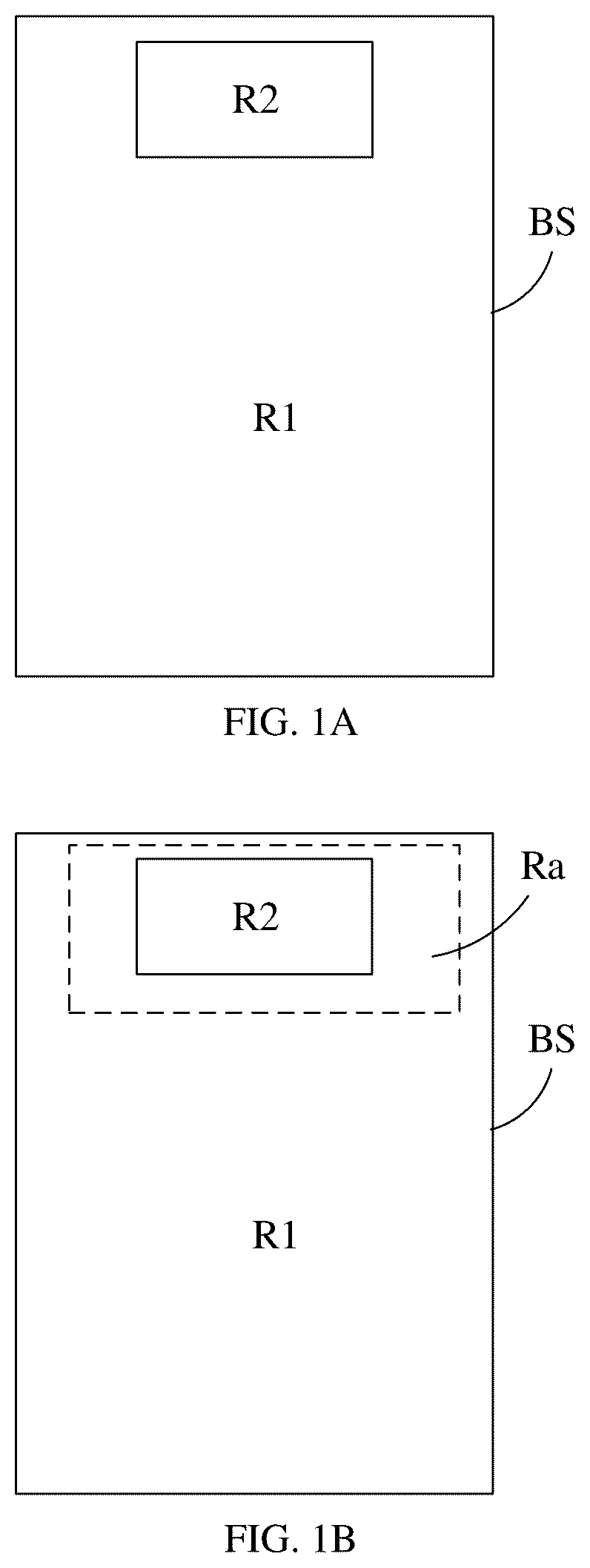
A is a schematic structural diagram of a display panel provided by an embodiment of the present disclosure. B is a schematic structural diagram of a display panel provided by an embodiment of the present disclosure. As illustrated in A and B , the display panel may include: a base substrate BS. The display panel includes a first display region R 1 and a second display region R 2 ; and the first display region R 1 may be located on at least one side of the second display region R 2 . For example, in some embodiments, the first display region R 1 surrounds the second display region R 2 . That is, the second display region R 2 may be surrounded by the first display region RE The second display region R 2 may also be arranged in other positions; and the arrangement position of the second display region R 2 may be determined as needed. For example, the second display region R 2 may be located in a top middle position of the base substrate BS, or may also be located in an upper left corner position or an upper right corner position of the base substrate BS. For example, a device such as a photosensitive sensor (e.g., a camera) is provided in the second display region R 2 of the display panel. For example, the second display region R 2 is a light-transmitting display region; and the first display region R 1 is a display region. For example, the first display region R 1 is opaque and only used for display. B illustrates that the first display region R 1 includes an auxiliary region Ra.
is a schematic diagram of a pixel unit of a display panel provided by an embodiment of the present disclosure. The display panel includes a pixel unit 100 ; and the pixel unit 100 is located on a base substrate. As illustrated in , the pixel unit 100 includes a pixel circuit 100 a and a light-emitting element 100 b ; and the pixel circuit 100 a is configured to drive the light-emitting element 100 b . For example, the pixel circuit 100 a is configured to supply a driving current to drive the light-emitting element 100 b to emit light. For example, the light-emitting element 100 b is an Organic Light-Emitting Diode (OLED); and the light-emitting element 100 b emits red light, green light, blue light, or white light, etc., under the driving of a pixel circuit 100 a corresponding thereto. A light-emitting color of the light-emitting element 100 b may be determined as needed.
In order to increase light transmittance of the second display region R 2 , the second display region R 2 may be provided with only light-emitting elements, while the pixel circuits for driving the light-emitting elements of the second display region R 2 may be provided in the first display region RE That is, the light transmittance of the second display region R 2 is increased by separately arranging the light-emitting element and the pixel circuit. That is, the second display region R 2 is not provided with the pixel circuit 100 a.
is a schematic diagram of a display panel provided by an embodiment of the present disclosure. As illustrated in , the display panel includes: a plurality of first-type pixel circuits 10 , a plurality of second-type pixel circuits 20 , and a plurality of first-region light-emitting elements 30 that are located in a first display region R 1 ; as well as a plurality of second-region light-emitting elements 40 located in a second display region R 2 . For example, the plurality of second-type pixel circuits 20 may be distributed at intervals among the plurality of first-type pixel circuits 10 .
For example, as illustrated in , at least one first-type pixel circuit 10 among the plurality of first-type pixel circuits 10 may be connected with at least one first-region light-emitting element 30 among the plurality of first-region light-emitting elements 30 ; and an orthographic projection of the at least one first-type pixel circuit 10 on the base substrate BS may at least partially overlap with an orthographic projection of the at least one first-region light-emitting element 30 on the base substrate BS. The at least one first-type pixel circuit 10 may be used to supply a drive signal to the first-region light-emitting element 30 connected therewith, to drive the first-region light-emitting element 30 to emit light.
For example, as illustrated in , at least one second-type pixel circuit 20 among the plurality of second-type pixel circuits 20 may be connected with at least one second-region light-emitting element 40 among the plurality of second-region light-emitting elements 40 through a conductive line L 1 ; and the at least one second-type pixel circuit 20 may be used to supply a drive signal to the second-region light-emitting element 40 connected therewith, to drive the second-region light-emitting element 40 to emit light. As illustrated in , because the second-region light-emitting element 40 and the second-type pixel circuit 20 are located in different regions, there is no overlapping portion between an orthographic projection of at least one second-type pixel circuit 20 on the base substrate BS and an orthographic projection of at least one second-region light-emitting element 40 on the base substrate BS.
For example, in the embodiment of the present disclosure, the first display region R 1 may be set as a non-transmitting display region; and the second display region R 2 may be set as a transmitting display region. For example, the first display region R 1 cannot transmit light; and the second display region R 2 can transmit light. In this way, the display panel provided by the embodiment of the present disclosure may have the required device structure such as the photosensitive sensor directly arranged in a position corresponding to the second display region R 2 on a side of the display panel, without performing digging process on the display panel to form a hole, which lays a solid foundation for implementing a true full screen. In addition, because the second display region R 2 only includes light-emitting elements and does not include pixel circuits, it is favorable for increasing light transmittance of the second display region R 2 , so that the display panel has a better display effect.
As illustrated in , the pixel unit 100 includes a first pixel unit 101 and a second pixel unit 102 ; the pixel circuit 100 a and the light-emitting element 100 b of the first pixel unit 101 are both located in the first display region R 1 ; the pixel circuit 100 a of the second pixel unit 101 is located in the first display region R 1 ; and the light-emitting element 100 b of the second pixel unit 102 is located in the second display region R 2 . In the embodiment of the present disclosure, the pixel circuit 100 a of the first pixel unit 101 is the first-type pixel circuit 10 ; the light-emitting element 100 b of the first pixel unit 101 is the first-region light-emitting element 30 ; the pixel circuit 100 a of the second pixel unit 101 is the second-type pixel circuit 20 ; and the light-emitting element 100 b of the second pixel unit 102 is the second-region light-emitting element 40 . For example, the first-region light-emitting element 30 may be referred to as an in-situ light-emitting element. For example, the first-type pixel circuit 10 may be referred to as an in-situ pixel circuit; and the second-type pixel circuit 20 may be referred to as an ex-situ pixel circuit.
For example, as illustrated in , the second-region light-emitting element 40 and the second-type pixel circuit 20 connected with the second-region light-emitting element 40 are located in a same row. That is, light-emitting signals of the second-region light-emitting elements 40 come from second-type pixel circuit in a same row. For example, pixel circuits of pixel units in a same row are connected with a same gate line.
As illustrated in , the pixel circuit (the second-type pixel circuit 20 ) of the second pixel unit 102 is connected with the light-emitting element (the second-region light-emitting element 40 ) of the second pixel unit 102 through a conductive line L 1 . For example, the conductive line L 1 is made of a transparent conductive material. For example, the conductive line L 1 is made of a conductive oxide material. For example, the conductive oxide material includes, but is not limited to, Indium Tin Oxide (ITO).
As illustrated in , one end of the conductive line L 1 is connected with the second-type pixel circuit 20 ; and the other end of the conductive line L 1 is connected with the second-region light-emitting element 40 . As illustrated in , the conductive line L 1 extends from the first display region R 1 to the second display region R 2 .
As illustrated in B and , in some embodiments, the first display region R 1 may include an auxiliary region Ra; and the auxiliary region Ra may be provided with the second-type pixel circuit 20 connected with the second-region light-emitting element 40 . For example, in a region of the first display region R 1 excluding the auxiliary region Ra, a plurality of dummy pixel circuits may be provided. The dummy pixel circuit is not connected with any light-emitting element. Providing the dummy pixel circuit is favorable for improving uniformity of components of respective film layers in an etching process. For example, the dummy pixel circuit has a same structure as the second-type pixel circuit 20 in a row or a column where it is located, except that it is not connected with any light-emitting element. For example, in the first display region R 1 , the auxiliary region Ra and the region of the first display region R 1 excluding the auxiliary region Ra (non-auxiliary region) have same pixel density, or same resolution, but it is not limited thereto.
illustrates three rows of light-emitting elements 100 b . A first row of light-emitting elements 100 b illustrated in passes through the first display region R 1 and the second display region R 2 , and is a row of light-emitting elements 100 b passing through two regions. A second row of light-emitting elements 100 b illustrated in passes through the first display region R 1 and the second display region R 2 , and is a row of light-emitting elements 100 b passing through two regions. A third row of light-emitting elements 100 b illustrated in only passes through the first display region R 1 but does not pass through the second display region R 2 , and is a row of light-emitting elements 100 b passing through one region. For example, in some embodiments, the light-emitting elements 100 b are divided into two types of row light-emitting elements, that is, a row of light-emitting elements passing through two regions and a row of light-emitting elements passing through one region.
is a schematic diagram of a first display region and a second display region in a display panel provided by an embodiment of the present disclosure. As illustrated in , in the second display region R 2 , a light-transmitting region R 0 is provided between adjacent second-region light-emitting elements 40 . For example, as illustrated in , a plurality of light-transmitting regions R 0 are connected with each other, to form a continuous light-transmitting region separated by a plurality of second-region light-emitting elements 40 . The conductive line L 1 is made of a transparent conductive material to increase light transmittance of the light-transmitting region R 0 as much as possible. As illustrated in , a region of the second display region R 2 except that provided with the second-region light-emitting element 40 may be a light-transmitting region.
A to C are partial plan views of a display panel provided by an embodiment of the present disclosure. A to C are described below.
A is a schematic diagram of a first display region and a second display region of a display panel provided by an embodiment of the present disclosure. As illustrated in A , the second display region R 2 is a light-transmitting display region; and the first display region R 1 is a display region.
B is a schematic diagram of a first-region light-emitting element in a first display region and a second-region light-emitting element in a second display region of a display panel provided by an embodiment of the present disclosure. B illustrates the first-region light-emitting element 30 and the second-region light-emitting element 40 .
Referring to A , B , and , in order to improve display effect, a density of the second-region light-emitting elements 40 may be equal to a density of the first-region light-emitting elements 30 . That is, a resolution of the second display region R 2 is the same as a resolution of the first display region RE Of course, in other embodiments, the density of the second-region light-emitting elements 40 may be greater or less than the density of the first-region light-emitting elements 30 . That is, the resolution of the second display region R 2 may be greater or less than the resolution of the first display region RE For example, as illustrated in B and , a light emission area of the second-region light-emitting element 40 is less than a light emission area of the first-region light-emitting element 30 . That is, the light emission area of the first-region light-emitting element 30 is greater than the light emission area of the second-region light-emitting element 40 . illustrates the light emission area of the second-region light-emitting element 40 and the light emission area of the first-region light-emitting element 30 with dotted lines. For example, the light emission area of the light-emitting element may correspond to an area of an opening of a pixel definition layer.
C illustrates the first-region light-emitting element 30 , the second-region light-emitting element 40 , the first-type pixel circuit 10 , the second-type pixel circuit 20 , the connecting element CE 0 , and the conductive line L 1 . Each pixel circuit is connected with a light-emitting element through a connecting element CE 0 . That is, each pixel unit has one connecting element CE 0 . That is, the first-type pixel circuit 10 is connected with the first-region light-emitting element 30 through a connecting element CE 0 ; and the second-type pixel circuit 20 is connected with the second-region light-emitting element 40 through a connecting element CE 0 .
For example, as illustrated in C , one end of the conductive line L 1 is connected with the second-region light-emitting element 40 ; and the other end of the conductive line L 1 is connected with the second-type pixel circuit 20 through the connecting element CE 0 . For example, the connecting element CE 0 is connected with the pixel circuit 100 a and the light-emitting element 100 b , respectively. For example, the connecting element CE 0 is connected with a light-emitting control transistor in the pixel circuit 100 a and a first electrode of the light-emitting element 100 b , respectively. For example, the connecting element CE 0 may be formed by a single conductive member, or may include two different conductive members located in different layers. For example, the connecting element CE 0 may include one conductive member located in one conductive layer and another conductive member located in another conductive layer.
As illustrated in C , a conductive line L 1 passes through a region where the pixel circuit of the pixel unit is located to respectively connect the second-type pixel circuit 20 and the second-region light-emitting element 40 on both sides of the pixel unit. For example, the region where the pixel circuit of the pixel unit is located overlaps with a plurality of conductive lines L 1 passing through the region. A region in the first display region R 1 where the second-type pixel circuit 20 is arranged may be referred to as an auxiliary region Ra (as illustrated in B and ); and the auxiliary region Ra may also be referred to as a transition region. C is described by taking that one first-type pixel circuit 10 overlaps with two conductive lines L 1 at most as an example; in other embodiments, one first-type pixel circuit 10 may also overlap with more conductive lines L 1 . For example, in some embodiments, one first-type pixel circuit 10 may overlap with 10 to 15 conductive lines L 1 . The number of conductive lines L 1 overlapping with one first-type pixel circuit 10 may be determined as needed. As illustrated in C , the second-type pixel circuit 20 may also overlap with the conductive line L 1 that is not connected with it.
In some embodiments, a pitch of the first-type pixel circuit 10 may be compressed in a first direction X to obtain a region where the second-type pixel circuit 20 is provided. For example, as illustrated in C , in the auxiliary region, a column of second-type pixel circuits 20 is arranged every other predetermined column of first-type pixel circuits 10 . For example, the number of columns of first-type pixel circuits 10 between two adjacent columns of second-type pixel circuits 20 may be determined as needed.
For example, in some embodiments, a pitch of the first-type pixel circuit 10 may be compressed in a first direction X to obtain a region where the second-type pixel circuit 20 is provided. For example, the pitch of the first-type pixel circuit 10 in the first direction X is less than a pitch of the first-region light-emitting element 30 in the first direction X. The first direction X is, for example, but is not limited to, a row direction. In other embodiments, the first direction X may also be a column direction. The embodiment of the present disclosure is described by taking the first direction X as a row direction.
D to F are schematic structural diagrams of display panels provided by some embodiments of the present disclosure. In order to further show that there are a plurality of extra columns of pixel circuits after the pixel circuit is compressed, D illustrates a schematic structural diagram of a first-region light-emitting element of a first display region RE E illustrates a schematic diagram of a portion of the structure (including only the pixel circuit) in A ; and F illustrates a schematic diagram of a portion of the structure (including only the light-emitting element) in A .
Referring to D to F , it may be seen that a width of the pixel circuit is less than a width of the light-emitting element. In this way, pixel circuits in the 2nd column and the 9th column from right to left are not connected with any first-region light-emitting element, which belong to the extra columns of pixel circuits, and may be used as the second-type pixel circuits 20 for connecting the second-region light-emitting elements 40 in the second display region R 2 . For example, as illustrated in F , the first-region light-emitting elements 30 may include first electrodes E 1 of 4 types of light-emitting elements RG 1 BG 2 ; and the first electrodes E 1 of the light-emitting elements are connected with the first-type pixel circuits 10 through a connecting element CE 0 . R refers to a light-emitting element emitting red light, G 1 refers to a light-emitting element emitting green light, B refers to a light-emitting element emitting blue light, and G 2 refers to a light-emitting element emitting green light. For example, the connecting element CE 0 includes two connecting electrodes, which may be respectively a connecting electrode CE 01 (as illustrated in E or B ) and a connecting electrode CE 02 (as illustrated in F or B ) mentioned later, but it is not limited thereto. For example, in order to provide sufficient space for arranging the conductive line L 1 , axes of the connecting electrodes CE 01 in a same row of pixel units may be located in a straight line.
F illustrates four rows of connecting elements CE 0 /connecting electrodes CE 02 , that is, F illustrates four rows of light-emitting elements. For example, light-emitting elements in each row are sequentially arranged in the first direction X in a manner of RGBG or BGRG. Of course, light-emitting colors of the light-emitting elements are not limited to RGB; arrangement mode of the light-emitting elements is not limited to that illustrated in F ; and the embodiment of the present disclosure is described by taking that the light-emitting element includes RGBG as an example. For example, as illustrated in F , G includes G 1 or G 2 . For example, in the pixel arrangement illustrated in F , one repeating unit RP includes two Gs arranged in a second direction Y and R and B respectively arranged on both sides of the two Gs in the first direction X, R and G constitute a pixel, and borrow B from another repeating unit adjacent thereto to constitute a virtual pixel for display; B and G constitute a pixel, and borrow R from another repeating unit adjacent thereto to constitute a virtual pixel for display, but it is not limited thereto.
Referring to , , and A to C , the display panel provided by some embodiments of the present disclosure includes: a base substrate BS, a plurality of light-emitting elements 100 b , and a plurality of pixel circuits 100 a . The base substrate BS has a first display region R 1 and a second display region R 2 ; and the first display region R 1 is located on at least one side of the second display region R 2 . The plurality of light-emitting elements 100 b are arranged in a plurality of rows and a plurality of columns.
Referring to , , C and F , the plurality of light-emitting elements 100 b includes a plurality of groups of light-emitting elements; light-emitting elements in each of the plurality of groups of light-emitting elements are arranged in the first direction X; and the plurality of groups of light-emitting elements are arranged in the second direction Y. and C both show three groups of light-emitting elements GP; the three groups of light-emitting elements GP are respectively one group of light-emitting elements GPx, one group of light-emitting elements GPy, and one group of light-emitting elements GPz; one group of light-emitting elements GPx and one group of light-emitting elements GPy pass through the first display region R 1 and the second display region R 2 ; and one group of light-emitting elements GPz only passes through the first display region R 1 . illustrates at least four groups of light-emitting elements GP arranged in the second direction Y. F illustrates at least four groups of light-emitting elements GP arranged in the second direction Y. In the display panel, the number of groups of light-emitting elements passing through the first display region R 1 and the second display region R 2 and the number of groups of light-emitting elements passing only through the first display region R 1 may be determined as needed.
For example, in some embodiments, one group of light-emitting elements may be one row of light-emitting elements. Of course, one group of light-emitting elements may not completely correspond to one column of light-emitting elements. In other embodiments, one group of light-emitting elements may be one column of light-emitting elements. Of course, one group of light-emitting elements may not completely correspond to one column of light-emitting elements. The embodiments of the present disclosure are described by taking one group of light-emitting elements as one row of light-emitting elements.
For example, referring to and C , at least one of the plurality of groups of light-emitting elements includes a plurality of first-region light-emitting elements 30 and a plurality of second-region light-emitting elements 40 . That is, at least one group of the plurality of groups of light-emitting elements passes through the first display region R 1 and the second display region R 2 .
For example, referring to , and C , the plurality of light-emitting elements 100 b include at least one row of light-emitting elements 100 b passing through two regions that passes through the first display region R 1 and the second display region R; and any row of light-emitting elements 100 b passing through two regions in the at least one row of light-emitting elements 100 b passing through two regions includes a plurality of first-region light-emitting elements 30 and a plurality of second-region light-emitting elements 40 .
For example, referring to , and C , a plurality of first-region light-emitting elements 30 are located in the first display region R 1 ; and a plurality of second-region light-emitting elements 40 are located in the second display region R 2 .
For example, referring to , C and E , the plurality of pixel circuits include a plurality of groups of pixel circuits GR; pixel circuits in each group of the plurality of pixel circuits are arranged in the first direction X; and the plurality of groups of pixel circuits are arranged in the second direction Y. For example, at least one group in the plurality of groups of pixel circuits 100 a includes a plurality of first-type pixel circuits 10 and a plurality of second-type pixel circuits 20 . and C respectively show three groups of pixel circuits GR. E illustrates four groups of pixel circuits GR. As illustrated in and C , the pixel circuit is only located in the first display region R 1 ; and no pixel circuit is provided in the second display region R 2 .
For example, referring to and C , a plurality of pixel circuits 100 a are arranged in a plurality of rows and a plurality of columns; and the plurality of pixel circuits 100 a include a plurality of first-type pixel circuits 10 and a plurality of second-type pixel circuits 20 located in a same row. In other words, at least one group of the plurality of groups of pixel circuits includes a plurality of first-type pixel circuits 10 and a plurality of second-type pixel circuits 20 .
For example, referring to and C , a plurality of first-type pixel circuits 10 and a plurality of second-type pixel circuits 20 are all located in the first display region R 1 ; and the plurality of second-type pixel circuits 20 are distributed at intervals between the plurality of first-type pixel circuits 10 . At least one first-type pixel circuit 10 among the plurality of first-type pixel circuits 10 is connected with at least one first-region light-emitting element 30 among the plurality of first-region light-emitting elements 30 ; an orthographic projection of the at least one first-type pixel circuit 10 on the base substrate BS at least partially overlaps with an orthographic projection of the at least one first-region light-emitting element 30 on the base substrate BS; and at least one second-type pixel circuit 20 among the plurality of second-type pixel circuits 20 is connected with at least one second-region light-emitting element 40 among the plurality of second-region light-emitting elements 40 through a conductive line.
A is a schematic diagram of a row of light-emitting elements located in a second display region and a second-type pixel circuit connected therewith in a display panel. B is a schematic diagram of capacitance of a conductive line in a display panel. C is a schematic diagram of display defect of a display panel. D to F are respectively schematic diagrams illustrating display defect in low gray scales. A is a schematic diagram of a row of light-emitting elements located in a second display region and a second-type pixel circuit connected therewith in a display panel provided by an embodiment of the present disclosure. B is a schematic diagram of capacitance of light-emitting elements emitting different colors of light in a same row of light-emitting elements located in a second display region of a display panel provided by an embodiment of the present disclosure.
For example, in the embodiment of the present disclosure, a row of light-emitting elements may refer to that pixel circuits connected with the row of light-emitting elements are all connected with the same gate line, but it is not limited thereto. For example, in the embodiment of the present disclosure, a row of pixel circuits may refer to that the row of pixel circuits are all connected with the same gate line, but it is not limited thereto. For example, in the embodiment of the present disclosure, a row of pixel units may refer to that the pixel circuits connected with the row of pixel units are all connected with the same gate line, but it is not limited thereto.
For example, as illustrated in A and A , in at least one group of light-emitting elements 100 b , the plurality of second-region light-emitting elements 40 include a plurality of first light-emitting elements 41 and a plurality of second light-emitting elements 42 ; the first light-emitting element 41 is configured to emit light of a first color; and the second light-emitting element 42 is configured to emit light of a second color. The plurality of second-type pixel circuits 20 include a plurality of first pixel circuits 21 and a plurality of second pixel circuits 22 ; the conductive lines L 1 include a plurality of first conductive lines La and a plurality of second conductive lines Lb; the plurality of light-emitting elements 41 are connected with the plurality of first pixel circuits 21 through a plurality of first conductive lines La; and the plurality of second light-emitting elements 42 are connected with the plurality of second pixel circuits 22 through a plurality of second conductive lines Lb. For example, one first light-emitting element 41 is connected with one first pixel circuit 21 through one first conductive line La; and one second light-emitting element 42 is connected with one second pixel circuit 22 through one second conductive line Lb.
For example, as illustrated in A and A , the plurality of second-region light-emitting elements 40 further include a plurality of third light-emitting elements 43 ; the third light-emitting elements 43 are configured to emit light of a third color; the plurality of second-type pixel circuits 20 further include a plurality of third pixel circuits 23 ; the conductive lines L 1 further include a plurality of third conductive lines Lc; and the plurality of third light-emitting elements 43 are connected with the plurality of third pixel circuits 23 through the plurality of third conductive lines Lc. For example, one third light-emitting element 43 is connected with one third pixel circuit 23 through one third conductive line Lc.
For example, as illustrated in A and A , the plurality of second-region light-emitting elements 40 further include a plurality of fourth light-emitting elements 44 ; the fourth light-emitting elements 44 are configured to emit light of a fourth color; the plurality of second-type pixel circuits 20 further include a plurality of fourth pixel circuits 24 ; the conductive lines L 1 further include a plurality of fourth conductive lines Ld; and the plurality of fourth light-emitting elements 44 are connected with the plurality of fourth pixel circuits 24 through the plurality of fourth conductive lines Ld. For example, one fourth light-emitting element 44 is connected with one fourth pixel circuit 24 through one fourth conductive line Ld.
For example, the light of a first color and the light of a fourth-color are both green light; one of the light of a second color and the light of a third color is red light; and the other of the light of a second color and the light of a third color is blue light.
For example, the fourth light-emitting element 44 and the first light-emitting element 41 are configured to emit light of the same color. For example, the fourth light-emitting element 44 and the first light-emitting element 41 are configured to emit green light; one of the second light-emitting element 42 and the third light-emitting element 43 is configured to emit red light; and the other of the second light-emitting element 42 and the third light-emitting element 43 is configured to emit blue light. The embodiment of the present disclosure is described by taking that the fourth light-emitting element 44 and the first light-emitting element 41 emit green light, the second light-emitting element 42 emits red light, and the third light-emitting element 43 emits blue light as an example; in other embodiments, the first light-emitting element 41 , the second light-emitting element 42 , the third light-emitting element 43 , and the fourth light-emitting element 44 may also emit light of other colors, which is not limited to the three colors of red, green and blue; and the color of light emitted by the first light-emitting element 41 , the second light-emitting element 42 , the third light-emitting element 43 , and the fourth light-emitting element 44 may be determined as needed.
As illustrated in B , an abscissa refers to a position of the second display region of the display panel in the first direction; and an ordinate refers to a ratio of capacitance of the conductive line connected with the light-emitting element in the position to total capacitance. In the display panel, capacitance difference of the conductive line varies greatly. Due to different lengths of the conductive lines connected with the respective light-emitting elements located in the second display region, capacitance difference of the light-emitting elements emitting light of different colors varies. As compared with capacitance difference of the conductive lines connected with light-emitting elements emitting red light and capacitance difference of the conductive lines connected with light-emitting elements emitting blue light, capacitance difference of the conductive lines connected with light-emitting elements emitting green light is greater. Because the capacitance difference of the conductive lines connected with light-emitting elements emitting green light is greater, light emission duration of the light-emitting elements emitting green light is reduced, so that brightness difference of the display panel occurs, resulting in display defect. For example, as illustrated in C , stripes appear when the display panel displays. For example, as illustrated in C , purple stripes appear when the display panel displays ( C is a gray-scale image, not marked with colors). For example, vertical purple stripes appear when the display panel displays. For example, as illustrated in D to F , at low gray scales, a defectiveness degree of the light-emitting element emitting green light is greater than a defectiveness degree of the light-emitting element emitting red light; a defectiveness degree of the light-emitting element emitting red light is greater than a defectiveness degree of the light-emitting element emitting blue light. For example, under the same gray scale, a driving current that drives the light-emitting element to emit blue light is greater than a driving current that drives the light-emitting element to emit red light; and a driving current that drives the light-emitting element to emit red light is greater than a driving current that drives the light-emitting element to emit green light.
B is a schematic diagram of capacitance distribution of conductive lines connected with light-emitting elements emitting light of different colors in a row of light-emitting elements located in the second display region corresponding to A . As illustrated in B , capacitance of the conductive line connected with the light-emitting element emitting green light is the smallest; and as illustrated in a left half of B , capacitance of the conductive line connected with the light-emitting element emitting green light presents a gradually increasing trend; so, capacitance difference of the two conductive lines connected with adjacent light-emitting elements emitting green light is smaller. Due to a symmetrical structure of the second display region of the display panel, a right half illustrated in B will not be described in details. As illustrated in B , the capacitance of the conductive line connected with the light-emitting element emitting green light is smaller than the capacitance of the conductive line connected with the light-emitting element emitting red light; and the capacitance of the conductive line connected with the light-emitting element emitting green light is smaller than the capacitance of the conductive line connected with the light-emitting element emitting blue light. As illustrated in B , the capacitance of the conductive line connected with the light-emitting element emitting red light presents a gradually increasing trend; and the capacitance of the conductive line connected with the light-emitting element emitting blue light presents a gradually increasing trend; and the capacitance of the conductive line connected with the light-emitting element emitting red light is not much different from the capacitance of the conductive line connected with the light-emitting element emitting blue light.
In the display panel provided by the embodiment of the present disclosure, in order to alleviate display defect, the arrangement order of the second-type pixel circuits connected with light-emitting elements emitting light of different colors is adjusted, to reduce or eliminate display defect caused by large differences in the lengths of the conductive lines. That is, when designing the second-type pixel circuits connected with the first light-emitting element, the lengths of the conductive lines and differences in the lengths of the conductive lines are considered, for example, a G-priority order is adopted. For example, G priority refers to that the second-type pixel circuits connected with the light-emitting element emitting green light is preferentially arranged close to the second display region.
As illustrated in A , in at least one group of light-emitting elements and at least one group of pixel circuits, the plurality of first pixel circuits 21 connected with the plurality of first light-emitting elements 41 are all closer to the second display region R 2 than each of the plurality of second pixel circuits 22 connected with the plurality of second light-emitting elements 42 . That is, as compared with the display panel illustrated in A , the display panel illustrated in A has the position of the first pixel circuit 21 connected with the first light-emitting element 41 adjusted, making the first pixel circuit 21 connected with the first light-emitting element 41 closer to the second display region R 2 than other second-type pixel circuits, so that the length difference of the first conductive line La connected with the first light-emitting element 41 is reduced, thereby reducing or avoiding display defect.
For example, in the embodiment of the present disclosure, being in at least one group of light-emitting elements and at least one group of pixel circuits, may refer to being in a row of light-emitting elements 100 b passing through two regions, or, may refer to being in a row of pixel units passing through two regions, but it is not limited thereto.
For example, as illustrated in A , in at least one group of light-emitting elements and at least one group of pixel circuits, no other second-type pixel circuit 20 is provided between two first pixel circuits 21 connected with two adjacent first conductive lines La. Such arrangement is favorable for reducing the lengths of the first conductive lines La, and is also favorable for reducing length difference between the first conductive lines La.
It should be noted that, in the display panel provided by the embodiment of the present disclosure, element A and element B being adjacent to each other, or adjacent element A and element B refers to that between element A and element B, there is no more element A or element B, but there may be other element besides element A and element B. Element A and element B may be the same element or different elements.
For example, as illustrated in C , E and A , in at least one group of light-emitting elements and at least one group of pixel circuits, at least one of the plurality of first-type pixel circuits 10 is arranged between two adjacent second-type pixel circuits 20 .
For example, as illustrated in A , in at least one group of light-emitting elements and at least one group of pixel circuits, the plurality of first pixel circuits 21 connected with the plurality of first conductive lines La are arranged at intervals among the plurality of first-type pixel circuits 10 ; and the plurality of second pixel circuits 22 connected with the plurality of second conductive lines Lb are arranged at intervals among the plurality of first-type pixel circuits 10 .
A only illustrates a row of light-emitting elements passing through two regions; it may be understood that an upper side, a lower side, or the upper side and the lower side of a row of light-emitting elements illustrated in A further include a plurality of rows of light-emitting elements the same as the row of light-emitting elements illustrated in the diagram. Thus, each light-emitting element illustrated in A is one of one column of light-emitting elements; and each pixel circuit illustrated in A is one of one column of pixel circuits.
For example, as illustrated in A , in at least one group of light-emitting elements and at least one group of pixel circuits, the plurality of first pixel circuits 21 connected with the plurality of first conductive lines La are all closer to the second display region R 2 than each of the plurality of third pixel circuits 23 connected with the plurality of third conductive lines Lc.
For example, as illustrated in A , in order to make the second conductive line Lb have a smaller capacitance difference, and to make the third conductive line Lc have a smaller capacitance difference, in at least one group of light-emitting elements and at least one group of pixel circuits, the plurality of second pixel circuits 22 connected with the plurality of second conductive lines Lb and the plurality of third pixel circuits 23 connected with the plurality of third conductive lines Lc are alternately arranged.
For example, as illustrated in A , in at least one group of light-emitting elements and at least one group of pixel circuits, the plurality of fourth pixel circuits 24 connected with the plurality of fourth conductive lines Ld are all closer to the second display region R 2 than each of the plurality of second pixel circuits 22 connected with the plurality of second conductive lines Lb. In the embodiment of the present disclosure, the fourth light-emitting element 44 and the first light-emitting element 41 emit light of the same color, so the plurality of fourth pixel circuits 24 are also preferentially arranged, that is, the plurality of fourth pixel circuits 24 are arranged closer to the second display region. Of course, in other embodiments, the fourth light-emitting element 44 may not be provided, and thus the fourth pixel circuit 24 does not need to be provided. For example, in this case, the pixels may be in a form of real RGB, but it is not limited thereto.
For example, as illustrated in A , in order to make the first conductive line La have a smaller capacitance difference and to make the fourth conductive line Ld have a smaller capacitance difference, in at least one group of light-emitting elements and at least one group of pixel circuits, the plurality of fourth pixel circuits 24 connected with the plurality of fourth conductive lines Ld and the plurality of first pixel circuits 21 connected with the plurality of first conductive lines La are alternately arranged.
For example, at least one selected from the group consisting of the first conductive line La, the second conductive line Lb, the third conductive line Lc, and the fourth conductive line Ld is made of a transparent conductive material.
C is a schematic diagram of a display panel provided by an embodiment of the present disclosure. As illustrated in C , the second display region R 2 of the display panel has an symmetrical shape, and has a first symmetry axis X 1 extending in the first direction X and a second symmetry axis X 2 extending in the second direction Y. For example, as illustrated in C , a plurality of conductive lines L 1 are arranged; and the plurality of conductive lines L 1 are symmetrical with respect to the first symmetry axis X 1 and are symmetrical with respect to the second symmetry axis X 2 . C only schematically illustrates four conductive lines L 1 . C illustrates that the second display region R 2 includes a first sub-region R 21 , a second sub-region R 22 , a third sub-region R 23 , and a fourth sub-region R 24 . The first sub-region R 21 and the second sub-region R 22 are symmetrical with respect to the second symmetry axis X 2 ; the third sub-region R 23 and the fourth sub-region R 24 are symmetrical with respect to the second symmetry axis X 2 ; the first sub-region R 21 and the third sub-region R 23 are symmetrical with respect to the first symmetry axis X 1 ; and the second sub-region R 22 and the fourth sub-region R 24 are symmetrical with respect to the first symmetry axis X 1 . For example, the plurality of second-region light-emitting elements are symmetrical with respect to the first symmetry axis X 1 and are symmetrical with respect to the second symmetry axis X 2 . The one row of light-emitting elements illustrated in A may be located in the first sub-region R 21 or the third sub-region R 23 .
A is a schematic diagram of a light-emitting element located in a second display region and a second-type pixel circuit connected therewith in a display panel provided by an embodiment of the present disclosure. A illustrates part of the light-emitting elements located in the second display region; for clarity of illustration, the light-emitting elements located in the first display region are omitted, and the first-type pixel circuits are omitted. Referring to A and A , it may be understood that one or more first-type pixel circuits and first-region light-emitting elements connected with the first-type pixel circuits are arranged between two adjacent second-type pixel circuits.
A illustrates two rows of light-emitting elements located in a left half of the second display region R 2 ; a structure in the second display region R 2 is symmetrical up and down with respect to an axis X 1 , and is symmetrical left and right with respect to the second symmetry axis X 2 . A illustrates two rows of light-emitting elements r 1 and r 2 ; and one row of light-emitting elements r 1 in A is used as a main object for description. For example, the two rows of light-emitting elements r 1 and r 2 are symmetrical with respect to the first symmetry axis X 1 . For example, the two rows of light-emitting elements r 1 and r 2 illustrated in A are respectively located in the first sub-region R 21 and the third sub-region R 23 illustrated in C .
B is a schematic diagram of the first conductive line La and the fourth conductive line Ld in A . C is a schematic diagram of the second conductive line Lb in A . D is a schematic diagram of the third conductive line Lc in A .
For example, in some embodiments, the first conductive line La and the fourth conductive line Ld are located in the same pattern layer; the second conductive line Lb is located in one pattern layer; and the third conductive line Ld is located in another pattern layer, thereby forming three pattern layers. For example, in some embodiments, the first conductive line La and the fourth conductive line Ld are located in the third pattern layer; the second conductive line Lb is located in the second pattern layer; and the third conductive line Ld is located in the first pattern layer. For example, the third pattern layer, the second pattern layer, and the first pattern layer are sequentially arranged in a direction perpendicular to the base substrate; the first pattern layer is closer to the base substrate than the second pattern layer; and the second pattern layer is closer to the base substrate than the third pattern layer. In the case where the number of conductive lines that need to be provided for each group of light-emitting elements is small, the conductive lines that need to be provided for the group of light-emitting elements may be arranged in one layer; and in the case where the number of conductive lines that need to be provided for each group of light-emitting elements is large, the conductive lines may be respectively arranged in several different layers; and according to needs, part of the conductive lines may be formed by segmentation, that is, formed by conductive portions located in different layers. In the case where there are more conductive lines to be provided, a mode of arranging by segmentation is adopted.
For example, as illustrated in A , B to D , the conductive lines connected with two adjacent rows of light-emitting elements 100 b passing through the two regions are axially symmetrical.
For example, as illustrated in A and B to D , the structure in the second display region R 2 is axially symmetrical.
E is a schematic diagram of a row of light-emitting elements r 1 of a display panel provided by another embodiment of the present disclosure. As illustrated in E , a solid line in the diagram indicates location in the second pattern layer; a single-dot dash indicates location in the first pattern layer; and a dashed line indicates location in the third pattern layer. Conductive portions of the same conductive line that are located in different layers are connected through via holes. As illustrated in E , in a densely wired region, in the second direction Y, adjacent conductive lines are located in different pattern layers; and such arrangement is favorable for reducing interference between the conductive lines.
For example, at least one selected from the group consisting of one of the plurality of first conductive lines La, one of the plurality of second conductive lines Lb, one of the plurality of third conductive lines Lc, and one of the plurality of fourth conductive lines Ld is formed integrally by one conductive line, or is formed by conductive portions located in different layers.
As illustrated in E , the conductive line Lb 1 is formed by conductive portions located in different layers; the conductive line Lc 1 is formed by conductive portions located in different layers; and other conductive lines in E are all formed integrally by one conductive line, and distributed in three different pattern layers.
For example, as illustrated in B , the first display region R 1 includes an auxiliary region Ra; a plurality of second-type pixel circuits 20 are located in the auxiliary region Ra; an area of the auxiliary region Ra is less than an area of the region of the first display region R 1 excluding the auxiliary region Ra.
For example, in order to facilitate arranging the second-type pixel circuit 20 in the first display region R 1 , a pitch of the first-type pixel circuit 10 in the first direction is less than a pitch of the first-region light-emitting element 30 in the first direction. For example, a pitch of the second-type pixel circuit 20 in the first direction is less than a pitch of the first-region light-emitting element 30 in the first direction. For example, the pitch of the first-type pixel circuit 10 in the first direction is equal to or substantially equal to the pitch of the second-type pixel circuit 20 in the first direction.
The display panel illustrated in A includes a fourth light-emitting element; in other embodiments, the display panel may not include a fourth light-emitting element. In a case where the display panel does not include the fourth light-emitting element, the fourth light-emitting element illustrated in A and the pixel circuit connected with the fourth light-emitting element may be removed, and positions of other components may be adjusted accordingly.
A is a schematic diagram of another display panel provided by an embodiment of the present disclosure. B is a schematic diagram of a display panel provided by another embodiment of the present disclosure. As illustrated in A , the fourth conductive line Ld and the first conductive line La are located on the same side of the row of light-emitting elements; and A is described by taking that the fourth conductive line Ld and the first conductive line La are located on an upper side of the row of light-emitting elements as an example. As illustrated in A , the fourth conductive line Ld partially overlaps with the first conductive line La. That is, an orthographic projection of the fourth conductive line Ld on the base substrate partially overlaps with an orthographic projection of the first conductive line La on the base substrate. As illustrated in B , the second conductive line Lb partially overlaps with the third conductive line Lc. That is, an orthographic projection of the second conductive line Lb on the base substrate partially overlaps with an orthographic projection of the third conductive line Lc on the base substrate. The overlapping arrangement of the conductive lines may help reduce space in the second display region that is occupied by the conductive lines connected with the row of light-emitting elements in the second direction Y, and facilitate arrangement of more conductive lines. As illustrated in A and B , the same line type indicates location in the same layer. For example, a portion illustrated by the single-dot dash indicates location in the first pattern layer L 11 ; a portion illustrated by the solid line indicates location in the second pattern layer L 12 ; and a portion illustrated by the dashed line indicates location in the third pattern layer L 13 . For example, the first pattern layer L 11 is closer to the base substrate than the second pattern layer L 12 ; and the second pattern layer L 12 is closer to the base substrate than the third pattern layer L 13 , but it is not limited thereto; a fabrication order of the respective pattern layers may also be adjusted as needed such that distances between the respective pattern layers and the base substrate are different from those in the previous description.
A to E are schematic diagrams of a display panel provided by an embodiment of the present disclosure. As illustrated in A to E , a row of light-emitting elements includes 48 second-region light-emitting elements; for clarity of illustration, not all of the second-region light-emitting elements are illustrated in a single diagram. A circle and a sign with a number in the circle indicate the second-region light-emitting element, and the number in the circle indicates a serial number of the second-region light-emitting element. Brackets and a sign with a number in the brackets indicate the second-type pixel circuit, and the number in the brackets indicate a serial number of the second-type pixel circuit. As illustrated in A , the second-region light-emitting element in the 48th column is connected with the second-type pixel circuit in the 25th column through a conductive line; for connection of remaining respective second-region light-emitting elements and second-type pixel circuits, the above description may be referred to. A to E are described by taking that the fourth light-emitting element 44 and the first light-emitting element 41 emit green light, the second light-emitting element 42 emits red light, and the third light-emitting element 43 emits blue light as an example; and the diagram illustrates that the second-region light-emitting elements are arranged in an order of RGBG. E illustrates G 1 (which may refer to the first light-emitting element 41 ) and G 2 (which may refer to the fourth light-emitting element 44 ), and thus, a form of RG 1 BG 2 is formed. In A to E , the conductive line connected with the first light-emitting element 41 (G 1 or G adjacent to B and located on the left side of B) is the first conductive line La; the conductive line connected with the second light-emitting element 42 (R) is the second conductive line Lb; the conductive line connected with the third light-emitting element 43 (B) is the third conductive line Lc; and the conductive line connected with the fourth light-emitting element 44 (G 2 or G adjacent to B and located on the right side of B) is the fourth conductive line Ld.
A illustrates the conductive line located in the first pattern layer L 11 ; A illustrates an entire conductive line and a first conductive portion L 01 for forming a conductive line; the first conductive portions L 01 are connected with the second-type pixel circuits in the 14th column to the 22nd column, respectively; and A illustrates 13 entire conductive lines and 9 first conductive portions L 01 .
B illustrates a conductive line located in the second pattern layer L 12 ; B illustrates an entire conductive line and a second conductive portion L 02 for forming a conductive line; the second conductive portions L 02 are respectively connected with 9 second-region light-emitting elements (odd-numbered light-emitting elements in the 31st column to the 47th column) illustrated in A ; and B illustrates 13 entire conductive lines and 9 second conductive portions L 02 .
C illustrates the conductive lines located in the third pattern layer L 13 ; C illustrates 13 entire conductive lines; and the 13 conductive lines are respectively connected with the second-region light-emitting elements from the 1st column to the 13th column.
D illustrates that the first conductive portion L 01 in A and the second conductive portion L 02 in B are connected through a via hole VO running through an insulating layer to form one conductive line. As illustrated in D , the third conductive line Lc may include a first conductive portion L 01 and a second conductive portion L 02 connected with each other; and the fourth conductive line Ld may include a first conductive portion L 01 and a second conductive portion L 02 connected with each other. As illustrated in D , the first conductive portion L 01 extends in the second direction Y; and the second conductive portion L 02 extends in the first direction X; in order to make adjacent conductive lines have a small capacitance difference, ends of a plurality of second conductive portions L 02 that are away from the second-region light-emitting element are flush with each other. For example, as illustrated in D , lengths of the plurality of first conductive portions L 01 in the second direction Y are different from each other.
Referring to E , a group of light-emitting elements includes a plurality of sub-groups of light-emitting elements sequentially arranged in the first direction X; and the plurality of sub-groups of light-emitting elements are located on the same side of a symmetry axis extending in the second direction Y of the second display region. For example, referring to E , a group of light-emitting elements includes a first sub-group of light-emitting elements GP 01 , a second sub-group of light-emitting elements GP 02 , and a third sub-group of light-emitting elements GP 03 . Of course, for other groups of light-emitting elements, the above-described mode of dividing light-emitting elements into a plurality of sub-groups may also be referred to.
For example, as illustrated in E , the first sub-group of light-emitting elements GP 01 includes the first to the thirteenth light-emitting elements located in the same group of light-emitting elements (the same group of second-region light-emitting elements); and the second sub-group of light-emitting elements GP 02 includes the fourteenth to the twenty-sixth light-emitting elements located in the same group of light-emitting elements (the same group of second-region light-emitting elements); the third sub-group of light-emitting elements GP 03 includes the twenty-seventh to the forty-eighth light-emitting elements located in the same group of light-emitting elements (the same group of second-region light-emitting elements). Of course, in other embodiments, the same group of light-emitting elements (the same group of second-region light-emitting elements) may also be provided with other number of light-emitting elements, which may be set as needed. Referring to C and E , the embodiment of the present disclosure is described by taking that the same group of light-emitting elements (the same group of second-region light-emitting elements) includes forty-eight light-emitting elements located on the left side of the second symmetry axis X 2 as an example.
For example, referring to C and E , the respective light-emitting elements in the first sub-group of light-emitting elements GP 01 are connected with the conductive lines L 1 located in the third pattern layer L 13 ; referring to B and E , the light-emitting elements in the second sub-group of light-emitting elements GP 02 are connected with the conductive lines L 1 located in the second pattern layer L 12 ; referring to A , B and E , part of light-emitting elements of the third sub-group of light-emitting elements GP 03 are connected through the conductive lines L 1 located in the first pattern layer L 11 ; another part of light-emitting elements of the third sub-group of light-emitting elements GP 03 are connected through conductive lines each of which is formed by a segment constituted by a first conductive portion L 01 located in the first pattern layer L 11 and a second conductive portion L 02 located in the second conductive layer L 12 .
Referring to E , a group of pixel circuits includes a plurality of sub-groups of pixel circuits sequentially arranged in the first direction X; and the plurality of sub-groups of pixel circuits are located on the same side of a symmetry axis extending in the second direction Y of the second display region. For example, referring to E , a group of pixel circuits includes a first sub-group of pixel circuits GR 01 to a seventh sub-group of pixel circuits GR 07 ; and the seventh sub-group of pixel circuits GR 07 is closer to the second display region than the first sub-group of pixel circuits GR 01 . Of course, for other groups of pixel circuits, the above-described mode of dividing pixel circuits into a plurality of sub-groups may also be referred to.
Referring to E , the conductive lines connected with the first sub-group of light-emitting elements GP 01 are located in the same layer; the conductive lines connected with the second sub-group of light-emitting elements GP 02 are located in the same layer; the conductive lines connected with the third sub-group of light-emitting elements GP 03 include a conductive line located in the same layer, and also include a conductive line formed in segments; and the conductive line formed in segments includes portions located in different layers.
Referring to E , the conductive lines connected with the first sub-group of light-emitting elements GP 01 are located in the third pattern layer L 13 ; the conductive lines connected with the second sub-group of light-emitting elements GP 02 are located in the second pattern layer L 12 ; the conductive lines connected with the third sub-group of light-emitting elements GP 03 include a conductive line located in the first pattern layer L 11 , and also include a conductive line formed in segments; and the conductive line formed in segments includes a first conductive portion L 01 located in the first pattern layer L 11 and a second conductive portion L 02 located in the second pattern layer L 12 .
Referring to E , the second light-emitting element 42 and the third light-emitting element 43 in the first sub-group of light-emitting elements GP 01 are connected with the second sub-group of pixel circuits GR 02 ; the second light-emitting element 42 and the third light-emitting element 43 in the second sub-group of light-emitting elements GP 02 are connected with the first sub-group of pixel circuits GR 01 ; the second light-emitting element 42 and the third light-emitting element 43 in the third sub-group of light-emitting elements GP 03 that are close to the second sub-group of light-emitting elements GP 02 are connected with the fourth sub-group of pixel circuits GR 04 ; the second light-emitting element 42 and the third light-emitting element 43 in the third sub-group of light-emitting elements GP 03 that are away from the second sub-group of light-emitting elements GP 02 are connected with the third sub-group of pixel circuits GR 03 ; the first light-emitting element 41 and the fourth light-emitting element 44 in the first sub-group of light-emitting elements GP 01 are connected with the seventh sub-group of pixel circuits GR 07 ; the first light-emitting element 41 and the fourth light-emitting element 44 in the second sub-group of light-emitting elements GP 02 are connected with the sixth sub-group of pixel circuits GR 06 ; and the first light-emitting element 41 and the fourth light-emitting element 44 in the third sub-group of light-emitting elements GP 03 are connected with the fifth sub-group of pixel circuits GR 05 .
As illustrated in E , in order to reduce an occupied area of the conductive lines, portions extending in the first direction X of two fourth conductive lines Ld located in different layers may at least partially overlap with each other. That is, orthographic projections of the portions extending in the first direction X of the two fourth conductive lines Ld located in different layers on the base substrate at least partially overlap with each other.
For example, in order to reduce the occupied area of the conductive lines, portions extending in the first direction X of two first conductive lines La located in different layers may at least partially overlap with each other. That is, orthographic projections of the portions extending in the first direction X of the two first conductive lines La located in different layers on the base substrate at least partially overlap with each other.
As illustrated in E , in order to reduce the occupied area of the conductive line, the portion extending in the first direction X of the fourth conductive line Ld may at least partially overlap with the portion extending in the first direction X of the first conductive line La that is located in a different layer from the portion extending in the first direction X of the fourth conductive line Ld. That is, an orthographic projection of the portion extending in the first direction X of the fourth conductive line Ld on the base substrate may at least partially overlap with an orthographic projection of the portion extending in the first direction X of the first conductive line La that is located in a different layer from the portion extending in the first direction X of the fourth conductive line Ld on the base substrate.
As illustrated in E , in order to reduce the occupied area of the conductive lines, the second conductive line Lb and the third conductive line Lc that are located in different layers partially overlap with each other. That is, an orthographic projection of the second conductive line Lb on the base substrate partially overlaps with an orthographic projection of the third conductive line Lc located in a different layer from the second conductive line Lb on the base substrate.
As illustrated in E , the third conductive lines Lc connected with the third sub-group of light-emitting elements GP 03 partially overlap with the second conductive lines Lb connected with the first sub-group of light-emitting elements GP 01 , that is, an orthographic projection of the third conductive lines Lc connected with the third sub-group of light-emitting elements GP 03 on the base substrate partially overlaps with an orthographic projection of the second conductive lines Lb connected with the first sub-group of light-emitting elements GP 01 on the base substrate.
As illustrated in E , the first conductive line La and the fourth conductive line Ld are located on the same side of the group of light-emitting elements. For example, as illustrated in E , an orthographic projection of a portion extending in the first direction X of one first conductive line La of the plurality of first conductive lines La on the base substrate at least partially overlaps with an orthographic projection of a portion extending in the first direction X of another first conductive line La located in a different layer from the first conductive line La on the base substrate; or an orthographic projection of a portion extending in the first direction X of one first conductive line La of the plurality of first conductive lines La on the base substrate at least partially overlaps with an orthographic projection of a portion extending in the first direction X of one fourth conductive line Ld of the plurality of fourth conductive lines Ld located in a different layer from the first conductive line La on the base substrate.
As illustrated in E , an orthographic projection of a portion extending in the first direction X of one second conductive line Lb of the plurality of second conductive lines Lb on the base substrate at least partially overlaps with an orthographic projection of a portion extending in the first direction X of one third conductive line Lc of the plurality of third conductive lines Lc located in a different layer from the second conductive line Lb on the base substrate.
As illustrated in E , a portion extending in the first direction of the conductive line L 1 connected with the second sub-group of light-emitting elements GP 02 does not overlap with a portion extending in the first direction of other conductive lines. Of course, the portion extending in the first direction of the conductive line L 1 connected with the second sub-group of light-emitting elements GP 02 may overlap with a portion extending in the second direction of other conductive lines. For example, the conductive lines L 1 connected with the second sub-group of light-emitting elements GP 02 are located in the second pattern layer L 12 ; the conductive lines L 1 connected with the first sub-group of light-emitting elements GP 01 are located in the third pattern layer L 13 ; and the conductive lines L 1 connected with the second light-emitting element 42 and the third light-emitting element 43 of the third sub-group of light-emitting elements GP 03 that are closer to the second sub-group of light-emitting elements GP 02 are located in the first pattern layer L 11 . As illustrated in E , the portion extending in the first direction of the conductive lines L 1 connected with the second sub-group of light-emitting elements GP 02 and the overlapping portions of two conductive lines overlapping with the portion extending in the first direction are alternately arranged. For example, the portion extending in the first direction of the conductive lines L 1 connected with the second sub-group of pixel circuits GR 02 overlaps with a portion extending in the first direction of the conductive lines L 1 connected with the fourth sub-group of pixel circuits GR 04 ; a portion extending in the first direction of the conductive lines L 1 connected with the first sub-group of pixel circuits GR 01 does not overlap with a portion extending in the first direction of the conductive lines L 1 connected with the second sub-group of pixel circuits GR 02 , and does not overlap with a portion extending in the first direction of the conductive line L 1 connected with the fourth sub-group of pixel circuits GR 04 . The conductive line in E includes a portion extending in the first direction X and portions extending in the second direction Y that are located on both sides of the portion extending in the first direction.
Referring to C and E , the conductive line connected with the second sub-group of pixel circuits GR 02 is located in the third pattern layer L 13 ; and the conductive line connected with the seventh sub-group of pixel circuits GR 07 is located in the second pattern layer L 12 .
Referring to B , D and E , the conductive lines connected with the first sub-group of pixel circuits GR 01 are located in the second pattern layer L 12 ; and the conductive lines connected with the sixth sub-group of pixel circuits GR 06 are located in the second pattern layer L 12 . The second conductive portions L 02 of the conductive lines connected with the third sub-group of pixel circuits GR 03 are located in the second pattern layer L 12 .
Referring to A and E , the conductive lines connected with the fifth sub-group of pixel circuits GR 05 are located in the first pattern layer L 11 ; and the conductive lines connected with the fourth sub-group of pixel circuits GR 04 are located in the first pattern layer L 11 . The first conductive portions L 01 of the conductive lines connected with the third sub-group of pixel circuits GR 03 are located in the first pattern layer L 11 .
Referring to A to E , the number of pixel circuits included in each sub-group of pixel circuits is as illustrated by the pixel circuits between two vertical dotted lines in the diagrams. It should be noted that, those skilled in the art may set the number of pixel circuits included by each sub-group of pixel circuits as needed. A to E are described by taking that the second display region includes 48 second-region light-emitting elements as an example, but it may also be set as needed.
Referring to A to E , for clarity of illustration, a first-type pixel circuit located between two second-type pixel circuits is omitted in the diagram, and the first-region light-emitting element connected with the first-type pixel circuit is omitted.
Referring to A , A , B , and A to E , in a group of pixel units, or in a row of pixel units, a distance between two adjacent second-type pixel circuits is greater than a distance between two adjacent second-region light-emitting elements.
For an arrangement mode of the second-type pixel circuits in the display panel illustrated in A to E , the arrangement mode of the second-type pixel circuits illustrated in A , A , A and B and related description may be referred to, and no details will be repeated here. The mode of arranging the pixel circuit connected with the first light-emitting element in the display panel illustrated in A to E closer to the second display region than other second-type pixel circuits is favorable for reducing capacitance of the conductive line of the first light-emitting element, and is favorable for reducing capacitance difference of conductive lines connected with adjacent first light-emitting elements, to alleviate display defect, and achieve a better display effect. The mode of arranging the pixel circuits connected with the second light-emitting elements in the display panel illustrated in A to E is also favorable for reducing capacitance of the conductive line of the second light-emitting element and reducing capacitance difference of conductive lines connected with adjacent second light-emitting elements, to alleviate display defect. The mode of arranging the conductive line connected with the third light-emitting element in the display panel illustrated in A to E is also favorable for reducing capacitance of the conductive line connected with the third light-emitting element and reducing capacitance difference of conductive lines connected with adjacent third light-emitting elements, to alleviate display defect. In a case where there are more conductive lines to be provided, the mode of arranging portions extending in the first direction of the conductive lines illustrated in A to E to overlap with each other may be adopted to reduce the occupied area of the conductive lines.
F is a schematic diagram of connecting elements in a column of second-type pixel circuits in a display panel provided by an embodiment of the present disclosure. As illustrated in F , the column of second-type pixel circuits may be a column of second-type pixel circuits in the third sub-group of pixel circuits GR 03 illustrated in E . As illustrated in F , the plurality of connecting elements CE 0 located in different groups of pixel circuits have the same pitch in the first direction X, to facilitate fabrication. F illustrates pixel circuits located in one column in the eight groups of pixel circuits GR arranged in the second direction Y, corresponding to eight connecting elements CE 0 . F is described by taking the second-type pixel circuit in the twenty-second column as an example.
G is a schematic diagram of a conductive line connected with a column of second-region light-emitting elements in a display panel provided by an embodiment of the present disclosure. As illustrated in G , the column of second-region light-emitting elements may be a column of light-emitting elements in the third sub-group of light-emitting elements GP 03 illustrated in E . F is described by taking the second-region light-emitting elements in the thirty-first column as an example. As illustrated in F , in the same column of light-emitting elements, a connection position between the first electrode of the light-emitting element and the conductive line L 1 is gradually away from the second symmetry axis X 2 and then gradually close to the second symmetry axis X 2 .
H is a schematic diagram of connecting elements in a column of second-type pixel circuits in a display panel provided by an embodiment of the present disclosure. As illustrated in H , the column of second-type pixel circuits may be a column of second-type pixel circuits in the third sub-group of pixel circuits GR 03 illustrated in E . As illustrated in H , pitches of the plurality of connecting elements CE 0 located in different groups of pixel circuits in the first direction X gradually change, for example, gradually decrease and then gradually increase, so as to facilitate arrangement of the conductive lines L 1 /first conductive portions of the conductive lines L 1 . H illustrates the pixel circuits located in one column in the eight groups of pixel circuits GR arranged in the second direction Y, corresponding to eight connecting elements CE 0 . H is described by taking the second-type pixel circuit in the twenty-second column as an example.
In the arrangement modes illustrated in F and G , or H and G , the conductive lines corresponding to different groups of light-emitting elements may be located in the same layer. Through the arrangement modes of conductive lines in the display panel illustrated in A to G , or H and G , those skilled in the art may know an arrangement mode of each group of light-emitting elements passing through the first display region and the second display region, and may know a mode of arranging the conductive lines. For example, overlapping of the conductive lines as described above refers to overlapping of the portions extending in the first direction X of the conductive lines, i.e., having a greater overlapping area or a greater overlapping length.
As illustrated in E , an entire conductive line located in the second pattern layer L 12 does not overlap with other conductive line in a large area. For example, a portion extending in the first direction of the entire conductive line located in the second pattern layer L 12 does not overlap with other conductive lines.
Referring to A , E , A , B and E , the second display region includes a first edge R 2 a , a second edge R 2 b , a third edge R 2 c , and a fourth edge R 2 d . For example, the first edge R 2 a , the second edge R 2 b , the third edge R 2 c , and the fourth edge R 2 d are edges of a quadrangle, respectively. A row of light-emitting elements overlap with the first edge R 2 a . Part of the conductive lines of the plurality of conductive lines pass through the second edge R 2 b intersecting with the first edge R 2 a from the second display region to the first display region. For example, the conductive line formed in segments passes through the second edge R 2 b intersecting with the first edge R 2 a from the second display region to the first display region.
For example, in the embodiment of the present disclosure, the conductive lines are not electrically connected with each other; and the two overlapping conductive lines are located in different layers. An insulating layer is arranged between the first pattern layer L 11 and the second pattern layer L 12 ; an insulating layer is arranged between the third pattern layer L 13 and the second pattern layer L 12 ; and an insulating layer is arranged between the first pattern layer L 11 and the pixel circuit.
In the embodiment of the present disclosure, the row of light-emitting elements or a row of light-emitting elements may also be replaced by a group of light-emitting elements or a group of pixel units. The row of pixel circuits or a row of pixel circuits may also be replaced by a group of pixel circuits or a group of pixel units.
is a schematic diagram of a display panel provided by an embodiment of the present disclosure. For example, as illustrated in , in the auxiliary region Ra, an orthographic projection of the conductive line L 1 on the base substrate BS overlaps with an orthographic projection of the first-type pixel circuit 10 on the base substrate BS. illustrates an arrangement mode of G priority. The auxiliary region Ra may also be regarded as a region where the conductive line L 1 is provided.
In the embodiment of the present disclosure, the first direction X and the second direction Y are both directions parallel with a main surface of the base substrate; and the third direction Z refers to a direction perpendicular to the main surface of the base substrate. For example, the main surface of the base substrate refers to the surface used to fabricate various components.
The display panel provided by the embodiments illustrated in the respective accompanying drawings of the present disclosure is described by taking that one conductive line L 1 is connected with one second-type pixel circuit and connected with one second-region light-emitting element as an example; in other embodiments, one conductive line may also be connected with a plurality of second-region light-emitting elements.
A is a schematic diagram of a pixel circuit in a display panel provided by an embodiment of the present disclosure. B is a layout diagram of a pixel circuit in a display panel provided by an embodiment of the present disclosure. C is a cross-sectional view taken along the line A-B of B . D is a layout diagram of a pixel circuit in a display panel provided by another embodiment of the present disclosure. E is a layout diagram of a pixel circuit in a display panel provided by another embodiment of the present disclosure.
The pixel circuit illustrated in A may be a low temperature polysilicon (LTPS) AMOLED pixel circuit commonly used in the related art.
A illustrates a pixel circuit of one pixel unit of the display panel. As illustrated in A , the pixel unit 100 includes the pixel circuit 100 a and the light-emitting element 100 b . The pixel circuit 100 a includes six switching transistors (T 2 -T 7 ), one driving transistor T 1 , and one storage capacitor Cst. The six switching transistors are respectively a data writing transistor T 2 , a threshold compensation transistor T 3 , a first light-emitting control transistor T 4 , a second light-emitting control transistor T 5 , a first reset transistor T 6 , and a second reset transistor T 7 . The light-emitting element 100 b includes a first electrode E 1 and a second electrode E 2 , and a light-emitting functional layer located between the first electrode E 1 and the second electrode E 2 . For example, the first electrode E 1 is an anode, and the second electrode E 2 is a cathode. Generally, the threshold compensation transistor T 3 and the first reset transistor T 6 reduce leakage current by adopting double-gate thin film transistors (TFT).
As illustrated in A , the display panel includes a gate line GT, a data line DT, a first power supply line PL 1 , a second power supply line PL 2 , a light-emitting control signal line EML, an initialization signal line INT, a reset control signal line RST, and the like. For example, the reset control signal line RST includes a first reset control signal line RST 1 and a second reset control signal line RST 2 . The first power supply line PL 1 is configured to provide a constant first voltage signal VDD to the pixel unit 100 , the second power supply line PL 2 is configured to provide a constant second voltage signal VSS to the pixel unit 100 , and the first voltage signal VDD is greater than the second voltage signal VSS. The gate line GT is configured to provide a scan signal SCAN to the pixel unit 100 , the data line DT is configured to provide a data signal DATA (data voltage VDATA) to the pixel unit 100 , the light-emitting control signal line EML is configured to provide a light-emitting control signal EM to the pixel unit 100 , the first reset control signal line RST 1 is configured to provide a first reset control signal RESET 1 to the pixel unit 100 , and the second reset control signal line RST 2 is configured to provide the scan signal SCAN to the pixel unit 100 . For example, in a row of pixel units, the second reset control signal line RST 2 can be connected with the gate line GT, so as to be supplied with the scan signal SCAN. Of course, the second reset control signal line RST 2 can be supplied with the second reset control signal RESET 2 . The first initialization signal line INT 1 is configured to provide a first initialization signal Vinit 1 to the pixel unit 100 . The second initialization signal line INT 2 is configured to provide a second initialization signal Vinit 2 to the pixel unit 100 . For example, the first initialization signal Vinit 1 and the second initialization signal Vinit 2 are constant voltage signals, and their magnitudes may be between the first voltage signal VDD and the second voltage signal VSS, but are not limited thereto. For example, the first initialization signal Vinit 1 and the second initialization signal Vinit 2 may both be less than or equal to the second voltage signal VSS. For example, in some embodiments, the first initialization signal line INT 1 and the second initialization signal line INT 1 are connected with each other, and are both configured to provide an initialization signal Vinit to the pixel unit 100 , that is, the first initialization signal line INT 1 and the second initialization signal line INT 2 are both referred to as an initialization signal line INT, and the first initialization signal Vinit 1 and the second initialization signal Vinit 2 are equal, and both are Vinit.
As illustrated in A , the driving transistor T 1 is electrically connected to the light-emitting element 100 b , and outputs a driving current to drive the light-emitting element 100 b to emit light under the control of the scan signal SCAN, the data signal DATA, the first voltage signal VDD, and the second voltage signal VSS.
For example, the light-emitting element 100 b includes an organic light emitting diode (OLED), and the light-emitting element 100 b emits red light, green light, blue light, or white light under the driving of its corresponding pixel circuit 100 a . For example, one pixel includes a plurality of pixel units. One pixel may include a plurality of pixel units that emit light of different colors. For example, one pixel includes a pixel unit that emits red light, a pixel unit that emits green light, and a pixel unit that emits blue light, but it is not limited to this. The number of pixel units included in a pixel and the light output of each pixel unit can be determined according to needs.
For example, as illustrated in A , a gate electrode T 20 of the data writing transistor T 2 is connected to the gate line GT, a first electrode T 21 of the data writing transistor T 2 is connected to the data line DT, and a second electrode T 22 of the data writing transistor T 2 is connected to a first electrode T 11 of the driving transistor T 1 .
For example, as illustrated in A , the pixel circuit 100 a further includes the threshold compensation transistor T 3 , a gate electrode T 30 of the threshold compensation transistor T 3 is connected to the gate line GT, a first electrode T 31 of the threshold compensation transistor T 3 is connected to a second electrode T 12 of the driving transistor T 1 , and a second electrode T 32 of the threshold compensation transistor T 3 is connected to a gate electrode T 10 of the driving transistor T 1 .
For example, as illustrated in A , the display panel further includes the light-emitting control signal line EML, and the pixel circuit 100 a further includes the first light-emitting control transistor T 4 and the second light-emitting control transistor T 5 . A gate electrode T 40 of the first light-emitting control transistor T 4 is connected to the light-emitting control signal line EML, a first electrode T 41 of the first light-emitting control transistor T 4 is connected to the first power supply line PL 1 , and a second electrode T 42 of the first light-emitting control transistor T 4 is connected to the first electrode T 11 of the driving transistor T 1 . A gate electrode T 50 of the second light-emitting control transistor T 5 is connected to the light-emitting control signal line EML, a first electrode T 51 of the second light-emitting control transistor T 5 is connected to the second electrode T 12 of the driving transistor T 1 , and a second electrode T 52 of the second light-emitting control transistors T 5 is connected to a first electrode E 1 of the light-emitting element 100 b.
As illustrated in A , the first reset transistor T 6 is connected to the gate electrode T 10 of the driving transistor T 1 and is configured to reset the gate electrode of the driving transistor T 1 , and the second reset transistor T 7 is connected to the first electrode E 1 of the light-emitting element 100 b and is configured to reset the first electrode E 1 of the light-emitting element 100 b . The first initialization signal line INT 1 is connected to the gate electrode of the driving transistor T 1 through the first reset transistor T 6 . The second initialization signal line INT 2 is connected to the first electrode E 1 of the light-emitting element 100 b through the second reset transistor T 7 . For example, the first initialization signal line INT 1 and the second initialization signal line INT 2 are connected to each other and are input with the same initialization signal, but it is not limited to this. In some embodiments, the first initialization signal line INT 1 and the second initialization signal line INT 2 may also be insulated from each other and configured to input signals respectively.
For example, as illustrated in A , a first electrode T 61 of the first reset transistor T 6 is connected to the first initialization signal line INT 1 , a second electrode T 62 of the first reset transistor T 6 is connected to the gate electrode T 10 of the driving transistor T 1 , a first electrode T 71 of the second reset transistor T 7 is connected to the second initialization signal line INT 2 , and a second electrode T 72 of the second reset transistor T 7 is connected to the first electrode E 1 of the light-emitting element 100 b . For example, as illustrated in A , a gate electrode T 60 of the first reset transistor T 6 is connected to the first reset control signal line RST 1 , and a gate electrode T 70 of the second reset transistor T 7 is connected to the second reset control signal line RST 2 .
As illustrated in A , the first power supply line PL 1 is configured to provide the first voltage signal VDD to the pixel circuit 100 a . The pixel circuit further includes the storage capacitor Cst, a first electrode Ca of the storage capacitor Cst is connected to the gate electrode T 10 of the driving transistor T 1 , and a second electrode Cb of the storage capacitor Cst is connected to the first power supply line PL 1 .
For example, as illustrated in A , the display panel further includes the second power supply line PL 2 , and the second power supply line PL 2 is connected to a second electrode E 2 of the light-emitting element 100 b.
A illustrates a first node N 1 , a second node N 2 , a third node N 3 , and a fourth node N 4 . For example, in some embodiments, referring to A , a capacitor is formed between the first node N 1 and the conductive line L 1 , and a capacitor is formed between the conductive line L 1 and the fourth node N 4 , that is, the conductive line L 1 is coupled with the first node N 1 and the fourth node N 4 , respectively, resulting in brightness differences and display defects (for example, forming stripes (Mura)), which affects the display quality.
As illustrated in B , the pixel circuit includes the driving transistor T 1 , and the driving transistor includes the gate electrode T 10 . Referring to B and C , the second electrode Cb of the storage capacitor Cst has an opening OPN 1 , and one end of the connecting electrode CE 1 is connected to the gate electrode T 10 of the driving transistor T 1 through the opening OPN 1 . The connection electrode CE 1 may also be referred to as a first gate signal line SL 1 . As illustrated in B , the first gate signal line SL 1 is connected to the gate electrode T 10 of the driving transistor T 1 .
As illustrated in B , the first gate signal line SL 1 is connected to the second gate signal line SL 2 . The gate electrode T 10 of the driving transistor T 1 , the first gate signal line SL 1 , and the second gate signal line SL 2 constitute a gate signal portion PT 1 . The potentials on the gate signal portion PT 1 are the same. Of course, in other embodiments, the second gate signal line SL 2 may not be provided, in this case, the gate electrode T 10 of the driving transistor T 1 and the first gate signal line SL 1 constitute the gate signal portion PT 1 . For example, the second gate signal line SL 2 is the second electrode T 62 of the first reset transistor T 6 .
Referring to B and C , in order to stabilize the potentials on the gate signal portion PT 1 , the display panel provided by the embodiment of the present disclosure provides a shield electrode SE and a constant voltage line L 0 , and the constant voltage line L 0 is configured to provide a constant voltage to the pixel circuit. The shield electrode SE is connected to the constant voltage line L 0 , so that the voltage on the shield electrode SE is stable and can play a shielding role to prevent the conductive line L 1 from affecting the potentials on the gate signal portion PT 1 . The orthographic projection of the first gate signal line SL 1 on the base substrate BS falls within the orthographic projection of the shield electrode SE on the base substrate BS.
Referring to B , D to E , in order to make the shield electrode play a better shielding effect and increase the shielding amount, the orthographic projection of the first gate signal line SL 1 on the base substrate BS completely falls within the orthographic projection of the shield electrode SE on the base substrate BS.
For example, in order to reduce display defects (mura) and improve the display effect, the distance between a boundary of the orthographic projection of the first gate signal line SL 1 on the base substrate BS and a boundary of the orthographic projection of the shield electrode SE on the base substrate BS is greater than or equal to 1.75 μm. Because the area occupied by the pixel unit is limited, the distance of the shield electrode SE beyond the first gate signal line SL 1 can be defined. For example, in some embodiments, in order to obtain a better shielding effect, the distance between the boundary of the orthographic projection of the first gate signal line SL 1 on the base substrate BS and the boundary of the orthographic projection of the shield electrode SE on the base substrate BS is greater than or equal to 2.33 μm.
As illustrated in B , the display panel further includes a block BK, and the block BK is connected to the first power supply line PL 1 . The threshold compensation transistor T 3 includes a first channel CN 1 and a second channel CN 2 , and the first channel CN 1 and the second channel CN 2 are connected by a conductive connection portion CP. The orthographic projection of the block BK on the base substrate BS at least partially overlaps with the orthographic projection of the conductive connection portion CP of the threshold compensation transistor T 3 on the base substrate BS. As illustrated in B , the block BK of the pixel unit of the adjacent column is used to shield the conductive connection portion CP of the threshold compensation transistor T 3 of the pixel unit of the current column.
For example, as illustrated in B , in the case where the display panel includes the second gate signal line SL 2 , the second gate signal line SL 2 is connected to the first gate signal line SL 1 , and the orthographic projection of the second gate signal line SL 2 on the base substrate BS falls within the orthographic projection of the block BK on the base substrate BS. For further example, the boundary of the orthographic projection of the block BK on the base substrate BS exceeds the boundary of the orthographic projection of the second gate signal line SL 2 on the base substrate BS. For example, the boundary of the orthographic projection of the block BK on the base substrate BS exceeds the boundary of the orthographic projection of the second gate signal line SL 2 on the base substrate BS by a distance greater than or equal to 1.75 μm. For example, the boundary of the orthographic projection of the block BK on the base substrate BS exceeds the boundary of the orthographic projection of the second gate signal line SL 2 on the base substrate BS by a distance greater than or equal to 2.33 μm. Of course, in other embodiments, the shield electrode SE can also be used to replace the role of the block BK, or the orthographic projection of the second gate signal line SL 2 on the base substrate BS not only falls within the orthographic projection of the block BK on the base substrate BS, but also falls within the orthographic projection of the shield electrode SE on the base substrate BS.
For example, the material of the first gate signal line SL 1 is different from the material of the second gate signal line SL 2 . For example, the material of the first gate signal line SL 1 includes a metal, and the material of the second gate signal line SL 2 includes a conductive material formed by conducting a semiconductor material.
For example, as illustrated in B , in order to save wiring, the first power supply line PL 1 serves as the constant voltage line L 0 . In other embodiments, in order to save wiring, the first initialization signal line INL 1 can also be used as the constant voltage line or the second initialization signal line INL 2 can also be used as the constant voltage line. Examples of the constant voltage line L 0 are not limited to the first power supply line PL 1 , the first initialization signal line INL 1 , and the second initialization signal line INL 2 , and any signal line that provides a constant voltage in the pixel circuit can be used as the constant voltage line L 0 . The embodiment of the present disclosure takes the first power supply line PL 1 as the constant voltage line L 0 as an example for description, and in the case where a signal line that provides a constant voltage other than the first power supply line PL 1 is used as the constant voltage line L 0 , the shape of the shield electrode SE may be adjusted so that it is connected to the signal line supplying a constant voltage.
For example, the orthographic projection of the conductive line L 1 on the base substrate BS partially overlaps with the orthographic projection of the pixel circuit (the first pixel circuit 10 ) of the first pixel unit 101 on the base substrate BS. For example, the shield electrode SE is located between the conductive line L 1 and the first gate signal line SL 1 . In the embodiment of the present disclosure, after the pixel circuit is formed, the shield electrode SE is formed, then the conductive line L 1 is formed, and then the light-emitting element is formed, so that the shield electrode SE is located between the conductive line L 1 and the first gate signal line SL 1 , and the shield electrode SE is located between the conductive line L 1 and the gate electrode T 10 of the driving transistor.
For example, the conductive line L 1 is disposed in the auxiliary region, and the conductive line L 1 is not disposed in the region other than the auxiliary region of the first display region, so that the orthographic projection of the pixel circuit (the first-type pixel circuit), which is in the region of the first display region except the auxiliary region, on the base substrate BS does not overlap with the orthographic projection of the conductive line L 1 on the base substrate BS.
For example, the orthographic projection of the conductive line L 1 on the base substrate BS partially overlaps with the orthographic projection of the first gate signal line SL 1 in the pixel circuit of the first pixel unit 101 on the base substrate BS.
Referring to C and B a buffer layer BL is disposed on the base substrate BS, an isolation layer BR is disposed on the buffer layer BL, an active layer LY 0 is disposed on the isolation layer BR, a first insulating layer ISL 1 is disposed on the active layer LY 0 , a first conductive layer LY 1 is disposed on the first insulating layer ISL 1 , a second insulating layer ISL 2 is disposed on the first conductive layer LY 1 , a second conductive layer LY 2 is disposed on the second insulating layer ISL 2 , a third insulating layer ISL 3 is disposed on the second conductive layer LY 2 , and a third conductive layer LY 3 is disposed on the third insulating layer ISL 3 . The third conductive layer LY 3 includes a connecting electrode CE 01 , and the connecting electrode CE 01 is connected to the second electrode T 52 of the second light-emitting control transistor T 5 through a via hole H 3 penetrating the first insulating layer ISL 1 , the second insulating layer ISL 2 , and the third insulating layer ISL 3 . A fourth insulating layer and a fifth insulating layer are disposed on the third conductive layer LY 3 , and a fourth conductive layer LY 4 is disposed on the fourth insulating layer and the fifth insulating layer. The fourth conductive layer LY 4 includes a connecting electrode CE 02 , and the connecting electrode CE 02 is connected to the connecting electrode CE 01 through a via hole H 22 that penetrates the fourth insulating layer and the fifth insulating layer. A sixth insulating layer is disposed on the fourth conductive layer LY 4 , and the light-emitting element 100 b (the second-region light-emitting element 30 ) is connected to the connection electrode CE 02 through a via hole penetrating the sixth insulating layer. The light-emitting element 100 b includes a first electrode E 1 , a second electrode E 2 , and a light-emitting functional layer located between the first electrode E 1 and the second electrode E 2 . For example, the connecting element CE 0 includes the connecting electrode CE 01 and the connecting electrode CE 02 .
As illustrated in B , one end of the connecting electrode CE 1 is connected to the gate electrode T 10 of the driving transistor T 1 through a via hole H 1 , and the other end of the connecting electrode CE 1 is connected to the second electrode T 62 of the first reset transistor T 6 through a via hole H 2 . One end of the connecting electrode CE 2 is connected to the first initialization signal line INL 1 through a via hole H 4 , and the other end of the connecting electrode CE 2 is connected to the first electrode T 61 of the first reset transistor T 6 through a via hole H 5 . One end of the connecting electrode CE 3 is connected to the second initialization signal line INL 2 through a via hole H 6 , and the other end of the connecting electrode CE 3 is connected to the first electrode T 71 of the second reset transistor T 7 through a via hole H 7 . The first power supply line PL 1 is connected to the first electrode T 41 of the first light-emitting control transistor T 4 through a via hole H 8 . The first power supply line PL 1 is connected to the second electrode Cb of the storage capacitor Cst through a via hole H 9 . The first power supply line PL 1 is connected to the block BK through a via hole Hk. The data line DT is connected to the first electrode T 21 of the data writing transistor T 2 through a via hole H 0 .
For example, in the manufacturing process of the display panel, a self-aligned process is adopted, and a semiconductor patterned layer is subject to a conductor process by using the first conductive layer LY 1 as a mask. The semiconductor pattern layer can be formed by patterning a semiconductor film. For example, the semiconductor pattern layer is heavily doped by ion implantation, so that the portion of the semiconductor pattern layer that is not covered by the first conductive layer LY 1 is conducted, and a source electrode region (the first electrode T 11 ) and a drain electrode region (the second electrode T 12 ) of the driving transistor T 1 , a source electrode region (the first electrode T 21 ) and a drain electrode region (the second electrode T 22 ) of the data writing transistor T 2 , a source electrode region (the first electrode T 31 ) and a drain electrode region (the second electrode T 32 ) of the threshold compensation transistor T 3 , a source electrode region (the first electrode T 41 ) and a drain electrode region (the second electrode T 42 ) of the first light-emitting control transistor T 4 , a source electrode region (the first electrode T 51 ) and a drain electrode region (the second electrode T 52 ) of the second light-emitting control transistor T 5 , a source electrode region (the first electrode T 61 ) and a drain electrode region (the second electrode T 62 ) of the first reset transistor T 6 , and a source electrode region (the first electrode T 71 ) and a drain electrode region (the second electrode T 72 ) of the second reset transistor T 7 are formed. The portion of the semiconductor pattern layer covered by the first conductive layer LY 1 retains semiconductor characteristics, and can form a channel region of the driving transistor T 1 , a channel region of the data writing transistor T 2 , a channel region of the threshold compensation transistor T 3 , a channel region of the first light-emitting control transistor T 4 , a channel region of the second light-emitting control transistor T 5 , a channel region of the first reset transistor T 6 , and a channel region of the second reset transistor T 7 . For example, as illustrated in B , the second electrode T 72 of the second reset transistor T 7 and the second electrode T 52 of the second light-emitting control transistor T 5 are formed as an integrated structure; the first electrode T 51 of the second light-emitting control transistor T 5 , the second electrode T 12 of the driving transistor T 1 , and the first electrode T 31 of the threshold compensation transistor T 3 are formed as an integrated structure; the first electrode T 11 of the driving transistor T 1 , the second electrode T 22 of the data writing transistor T 2 , and the second electrode T 42 of the first light-emitting control transistor T 4 are formed as an integrated structure; and the second electrode T 32 of the threshold compensation transistor T 3 and the second electrode T 62 of the first reset transistor T 6 are formed as an integrated structure. In some embodiments, as illustrated in B , the first electrode T 71 of the second reset transistor T 7 and the first electrode T 61 of the first reset transistor T 6 may be formed as an integrated structure.
For example, the channel regions of the transistors used in the embodiment of the present disclosure may adopt monocrystalline silicon, polycrystalline silicon (such as low temperature polysilicon), or metal oxide semiconductor materials (such as IGZO, AZO, etc.). In one embodiment, the transistors are all P-type low temperature polysilicon (LTPS) thin film transistors. In another embodiment, the threshold compensation transistor T 3 and the first reset transistor T 6 , that are directly connected to the gate electrode of the driving transistor T 1 , are metal oxide semiconductor thin film transistors, that is, the channel material of the transistor is a metal oxide semiconductor material (such as IGZO, AZO, etc.). The metal oxide semiconductor thin film transistor has a lower leakage current, which can help reduce the leakage current of the gate electrode of the driving transistor T 1 .
For example, the transistors adopted in the embodiments of the present disclosure may include various structures, such as a top gate type, a bottom gate type, or a dual-gate structure. In one embodiment, the threshold compensation transistor T 3 and the first reset transistor T 6 , which are directly connected to the gate electrode of the driving transistor T 1 , are dual-gate thin film transistors, which can help reduce the leakage current of the gate electrode of the driving transistor T 1 .
For example, the display panel further includes a pixel definition layer and a spacer. The pixel definition layer has an opening, and the opening of the pixel definition layer is configured to define the light-emitting area (light exit region, effective light-emitting area) of the pixel unit. The spacer is configured to support a fine metal mask when forming the light-emitting functional layer.
For example, the opening is the light exit region of the pixel unit. The light-emitting functional layer is located on the first electrode E 1 of the light-emitting element 100 b , and the second electrode E 2 of the light-emitting element 100 b is located on the light-emitting functional layer. For example, an encapsulation layer is disposed on the light-emitting element 100 b . The encapsulation layer includes a first encapsulation layer, a second encapsulation layer, and a third encapsulation layer. For example, the first encapsulation layer and the third encapsulation layer are inorganic material layers, and the second encapsulation layer is an organic material layer. For example, the first electrode E 1 is the anode of the light-emitting element 100 b , and the second electrode E 2 is the cathode of the light-emitting element 100 b , but it is not limited thereto.
D is a layout diagram of a first-type pixel circuit or a second-type pixel circuit in a display panel provided by an embodiment of the present disclosure. For example, as illustrated in D , the orthographic projection of the gate electrode T 10 of the driving transistor T 1 on the base substrate BS falls within the orthographic projection of the shield electrode SE on the base substrate BS.
For example, as illustrated in D , in the case where the display panel includes the second gate signal line SL 2 , the second gate signal line SL 2 is connected to the first gate signal line SL 1 , and the orthographic projection of the second gate signal line SL 2 on the base substrate BS also falls within the orthographic projection of the shield electrode SE on the base substrate BS. For further example, the boundary of the orthographic projection of the shield electrode SE on the base substrate BS exceeds the boundary of the orthographic projection of the second gate signal line SL 2 on the base substrate BS. For example, the boundary of the orthographic projection of the shield electrode SE on the base substrate BS exceeds the boundary of the orthographic projection of the second gate signal line SL 2 on the base substrate BS by a distance greater than or equal to 1.75 μm. For example, the boundary of the orthographic projection of the shield electrode SE on the base substrate BS exceeds the boundary of the orthographic projection of the second gate signal line SL 2 on the base substrate BS by a distance greater than or equal to 2.33 μm.
For example, as illustrated in D , the orthographic projections of the gate electrode T 10 of the driving transistor T 1 , the first gate signal line SL 1 , and the second gate signal line SL 2 on the base substrate BS all fall into the orthographic projection of the shield electrode SE on the base substrate BS.
For example, as illustrated in D , the orthographic projection of the shield electrode SE on the base substrate BS partially overlaps with the orthographic projection of the second gate signal line SL 2 on the base substrate BS, and the orthographic projection of the block BK on the base substrate BS partially overlaps with the orthographic projection of the second gate signal line SL 2 on the base substrate BS. Thus, in the display panel illustrated in D , the shield electrode SE and the block BK form a double-layer shield for the second gate signal line SL 2 .
For example, as illustrated in D , the orthographic projection of the shield electrode SE on the base substrate BS partially overlaps with the orthographic projection of the block BK on the base substrate BS.
Of course, in other embodiments, the block BK may not be provided, or the orthographic projection of the block BK on the base substrate BS does not overlap with the orthographic projection of the second gate signal line SL 2 on the base substrate BS.
E is a layout diagram of a first-type pixel circuit or a second-type pixel circuit in a display panel provided by an embodiment of the present disclosure. As illustrated in E , the fourth conductive layer LY 4 further includes a third power supply line PL 3 . The third power supply line PL 3 is formed integrally with the shield electrode SE. The third power supply line PL 3 is connected to the first power supply line PL 1 through a via hole H 21 to form a parallel structure to reduce resistance. The third power supply line PL 3 extends in the second direction Y. As illustrated in E , the size of the third power supply line PL 3 in the second direction Y is larger than the size of the shield electrode SE in the second direction Y.
For example, as illustrated in B , and E , the orthographic projection of the block BK on the base substrate BS partially overlaps with the orthographic projection of the second gate signal line SL 2 on the base substrate BS, and the orthographic projection of the shield electrode SE on the base substrate BS partially overlaps with the orthographic projection of the first gate signal line SL 1 on the base substrate BS, so that the block BK and the shield electrode SE jointly function as a shield for the gate signal portion PT 1 . Of course, in other embodiments, the block BK may not be provided, or the orthographic projection of the block BK on the base substrate BS dose not overlap with the orthographic projection of the second gate signal line SL 2 on the base substrate BS.
For example, as illustrated in B , and E , the block BK on the left extends to a pixel unit on the left side of the pixel unit illustrated in the figure, in order to shield the conductive connection portion CP of the threshold compensation transistor T 3 , while the block BK on the right is extended from the block BK connected to a pixel unit on the right side of the pixel unit illustrated in the figure.
As illustrated in B , D , and E , the channel of each transistor as well as the first electrode and the second electrode on both sides of the channel are located in the active layer LY 0 ; the first reset control signal line RST 1 , the gate line GT, the gate electrode T 10 of the driving transistor (the first electrode Ca of the storage capacitor Cst), the light-emitting control signal line EML and the second reset control signal line RST 2 are located in the first conductive layer LY 1 ; the first initialization signal line INL 1 , the second electrode Cb of the storage capacitor Cst, and the second initialization signal line INL 2 are located in the second conductive layer LY 2 ; the data line DT, the first power supply line PL 1 , the connecting electrode CE 1 , the connecting electrode CE 2 , the connecting electrode CE 3 , and the connecting electrode CE 01 are located in the third conductive layer LY 3 ; and the shield electrode SE is located in the fourth conductive layer LY 4 . As illustrated in E , the shield electrode SE and the third power supply line PL 3 are located in the fourth conductive layer LY 4 .
As illustrated in B , D , and E , the first initialization signal line INL 1 , the first reset control signal line RST 1 , the gate line GT, the light-emitting control signal line EML, the second initialization signal line INL 2 , and the second reset control signal lines RST 2 all extend in the first direction X. As illustrated in B , D , and E , the data line DT and the first power supply line PL 1 both extend in the second direction Y.
In the embodiments of the present disclosure, an orthographic projection of an element A on the base substrate BS falls within an orthographic projection of an element B on the base substrate BS means that the orthographic projection of the element A on the base substrate BS completely falls into the orthographic projection of the element B on the base substrate BS, that is, the orthographic projection of the element B on the base substrate BS covers the orthographic projection of the element A on the base substrate BS, and the area of the orthographic projection of the element A on the base substrate BS is less than or equal to the area of the orthographic projection of the element B on the base substrate BS.
For example, in some embodiments of the present disclosure, each pixel circuit 100 a is provided with any one of the shield electrodes SE described above. That is, both the first-type pixel circuit 10 of the first pixel unit 101 and the second-type pixel circuit 20 of the second pixel unit 102 are provided with any one of the shield electrodes SE described above, but it is not limited thereto. For example, in some embodiments, the shield electrodes SE is not provided in each pixel circuit 100 a.
For example, the transistors in the pixel circuit of the embodiment of the present disclosure are all thin film transistors. For example, the first conductive layer LY 1 , the second conductive layer LY 2 , the third conductive layer LY 3 , and the fourth conductive layer LY 4 are all made of metal materials. For example, the first conductive layer LY 1 and the second conductive layer LY 2 are formed of metal materials such as nickel and aluminum, etc., but are not limited thereto. For example, the third conductive layer LY 3 and the fourth conductive layer LY 4 are formed of materials such as titanium, aluminum, etc., but are not limited thereto. For example, the third conductive layer LY 3 and the fourth conductive layer LY 4 are respectively a structure formed by three sub-layers of Ti/AL/Ti, but are not limited thereto. For example, the base substrate may be a glass substrate or a polyimide substrate, but it is not limited to this, and can be selected as required. For example, the buffer layer BL, the isolation layer BR, the first insulating layer ISL 1 , the second insulating layer ISL 2 , the third insulating layer ISL 3 , the fourth insulating layer IS 4 , the fifth insulating layer, and the sixth insulating layer are all made of insulating materials. The materials of the first electrode E 1 and the second electrode E 2 of the light-emitting element can be selected as required. In some embodiments, the first electrode E 1 may adopt at least one of transparent conductive metal oxide and silver, but it is not limited thereto. For example, the transparent conductive metal oxide includes indium tin oxide (ITO), but is not limited thereto. For example, the first electrode E 1 may adopt a structure in which three sub-layers of ITO-Ag-ITO are arranged. In some embodiments, the second electrode E 2 may adopt a metal of low work function, for example at least one of magnesium and silver, but is not limited thereto.
For example, referring to the layout diagrams and the cross-sectional views of the embodiment of the present disclosure, the display panel provided by at least one embodiment of the present disclosure can be manufactured by the following method.
•
• (1) Forming a buffer layer BL and an isolation layer BR on the base substrate BS. • (2) Forming a semiconductor film on the isolation layer BR. • (3) Patterning the semiconductor film to form a semiconductor pattern layer. • (4) Forming a first insulating film on the semiconductor pattern layer. • (5) Forming a first conductive film on the first insulating film, and patterning the first conductive film to form the first conductive layer LY 1 . • (6) Dopping the semiconductor pattern layer by using the first conductive layer LY 1 as a mask, so as to form the active layer LY 0 . • (7) Forming a second insulating film on the first conductive layer LY 1 . • (8) Forming a second conductive film on the second insulating layer ISL 2 , and patterning the second conductive film to form the second conductive layer LY 2 . • (9) Forming a third insulating film on the second conductive layer LY 2 . • (10) Patterning at least one of the first insulating film, the second insulating film, and the third insulating film to simultaneously form via holes, the first insulating layer ISL 1 , the second insulating layer ISL 2 , and the third insulating layer ISL 3 . • (11) Forming a third conductive film, and patterning the third conductive film to form the third conductive layer LY 3 ; the components in the third conductive layer LY 3 being connected to the components located under the third conductive layer LY 3 through the via holes. • (12) Forming a fourth insulating film and a fifth insulating film, and patterning the fourth insulating film and the fifth insulating film to simultaneously form via holes, the fourth insulating layer and the fifth insulating layer. • (13) Forming a fourth conductive film, and patterning the fourth conductive film to form the fourth conductive layer LY 4 . • (14) Forming at least one insulating layer and at least one transparent conductive layer, and the transparent conductive layer including the conductive lines L 1 . • (15) Forming a first electrode E 1 of the light-emitting element. • (16) Forming a pixel definition layer and a spacer. • (17) Forming a light-emitting functional layer. • (18) Forming a second electrode E 2 of the light-emitting element. • (19) Forming an encapsulation layer CPS.
Of course, in the display panel provided by the embodiment of the present disclosure, the shield electrode SE may not be provided.
At least one embodiment of the present disclosure provides a display device, including any one of the above-described display panels.
A and B are schematic diagrams of a display device provided by an embodiment of the present disclosure. As illustrated in A and B , a sensor SS is located on a side of the display panel DS and located in a second display region R 2 . Ambient light may be transmitted through the second display region R 2 and sensed by the sensor SS. As illustrated in B , a side of the display panel where the sensor SS is not provided is a display side, which may display images. For example, the sensor includes a photosensitive sensor; and the photosensitive sensor is located on a side of the display panel.
For example, the second display region R 2 may be rectangular, and an area of an orthographic projection of the sensor SS on the base substrate BS may be less than or equal to an area of an inscribed circle of the second display region R 2 . That is, a pitch of a region where the sensor SS is located may be less than or equal to a pitch of the inscribed circle of the second display region R 2 . For example, the pitch of the region where the sensor SS is located is equal to the pitch of the inscribed circle of the second display region R 2 , that is, a shape of the region where the sensor SS is located may be circular, and correspondingly, the region where the sensor SS is located may also be referred to as a light-transmitting hole. Of course, in some embodiments, the second display region R 2 may also have a shape other than a rectangle, for example, a circle or an ellipse.
For example, the display device is a full-screen display device with an under-screen camera. For example, the display device includes products or components with display function that including the above-mentioned display panel, such as a TV, a digital camera, a mobile phone, a watch, a tablet computer, a laptop computer, a navigator, and the like.
is a working timing diagram of the pixel circuit illustrated in A . As illustrated in , during one frame of display period, the driving method of the pixel unit includes a first reset stage t 1 , a data writing, threshold compensation and second reset stage t 2 , and a light-emitting stage t 3 . When the reset control signal RESET is at a low level, the gate electrode of the driving transistor T 1 is reset, and when the scan signal SCAN is at a low level, the first electrode E 1 (for example, the anode) of the light-emitting element 100 b is reset. For example, as illustrated in A , when the scan signal SCAN is at a low level, the data voltage VDATA is written, and the threshold voltage Vth of the driving transistor T 1 is obtained at the same time, and the data voltage VDADA containing the data information on the data line is stored in the capacitor Cst. When the light-emitting control signal line EML is at a low level, the light-emitting element 100 b emits light, and the voltage of the first node N 1 (node of the gate electrode) is maintained by the storage capacitor Cst (the light-emitting stability of the light-emitting element 100 b ). In the driving process of the pixel circuit 10 , in the light-emitting stage, the storage capacitor is used to maintain the voltage signal, so that the potential of the signal holding terminal can be kept constant, and a voltage is formed between the gate electrode and the source electrode of the driving transistor, thereby controlling the driving transistor to form a driving current, and then driving the light-emitting element 100 b to emit light.
As illustrated in , in the reset stage t 1 , the light-emitting control signal EM is set to a turn-off voltage, the reset control signal RESET is set to a turn-on voltage, and the scan signal SCAN is set to the turn-off voltage.
As illustrated in , in the data writing, threshold compensation and second reset stage t 2 , the light-emitting control signal EM is set to the turn-off voltage, the reset control signal RESET is set to the turn-off voltage, and the scan signal SCAN is set to the turn-on voltage.
As illustrated in , in the light-emitting stage t 3 , the light-emitting control signal EM is set to the turn-on voltage, the reset control signal RESET is set to the turn-off voltage, and the scan signal SCAN is set to the turn-off voltage.
As illustrated in , the first voltage signal ELVDD and the second voltage signal ELVSS are both constant voltage signals. For example, the level of the initialization signal Vinit is between the level of the first voltage signal ELVDD and the level of the second voltage signal ELVSS.
For example, the turn-on voltage in the embodiment of the present disclosure refers to a voltage that can electrically connect the first electrode and the second electrode of the corresponding transistor (the transistor is in ON state), and the turn-off voltage refers to a voltage that can electrically disconnect the first electrode and the second electrode of the corresponding transistor (the transistor is in OFF state). In the case where the transistor is a P-type transistor, the turn-on voltage is a low voltage (for example, 0V), and the turn-off voltage is a high voltage (for example, 5V); and in the case where the transistor is an N-type transistor, the turn-on voltage is a high voltage (for example, 5V) and the turn-off voltage is a low voltage (for example, 0V). The driving waveforms illustrated in are all explained by taking the P-type transistor as an example. For example, the turn-on voltage is a low voltage (for example, 0V), and the turn-off voltage is a high voltage (for example, 5V), but it is not limited to this.
Please refer to A and together. In the first reset stage t 1 , the light-emitting control signal EM is of the turn-off voltage, the reset control signal RESET is of the turn-on voltage, and the scan signal SCAN is of the turn-off voltage. At this time, the first reset transistor T 6 is in an ON state, and the second reset transistor T 7 , the data writing transistor T 2 , the threshold compensation transistor T 3 , the first light-emitting control transistor T 4 , and the second light-emitting control transistor T 5 are in an OFF state. The first reset transistor T 6 transmits the first initialization signal (initialization voltage Vinit) Vinit 1 to the gate electrode of the driving transistor T 1 , and the first initialization signal Vinit 1 is stored by the storage capacitor Cst. The driving transistor T 1 is reset, and the data stored during the last (previous frame) light-emitting is erased.
In the data writing, threshold compensation, and second reset stage t 2 , the light-emitting control signal EM is of the turn-off voltage, the reset control signal RESET is of the turn-off voltage, and the scan signal SCAN is of the turn-on voltage. At this time, the data writing transistor T 2 and the threshold compensation transistor T 3 are in the ON state, the second reset transistor T 7 is in the ON state, and the second reset transistor T 7 transmits the second initialization signal (initialization voltage Vinit) Vinit 2 to the first electrode E 1 of the light-emitting element 100 b to reset the light-emitting element 100 b . The first light-emitting control transistor T 4 , the second light-emitting control transistor T 5 , and the first reset transistor T 6 are in the OFF state. At this time, the data writing transistor T 2 transmits the data voltage VDATA to the first electrode of the driving transistor T 1 , that is, the data writing transistor T 2 receives the scan signal SCAN and the data voltage VDATA and writes the data voltage VDATA to the first electrode of the driving transistor T 1 according to the scan signal SCAN. The threshold compensation transistor T 3 is turned on to connect the driving transistor T 1 into a diode structure, thereby charging the gate electrode of the driving transistor T 1 . After the charging is completed, the voltage of the gate electrode of the driving transistor T 1 is VDATA+Vth, where VDATA is the data voltage and Vth is the threshold voltage of the driving transistor T 1 , that is, the threshold compensation transistor T 3 receives the scan signal SCAN and performs threshold voltage compensation to the gate electrode of the driving transistor T 1 according to the scan signal SCAN. During this stage, the voltage difference between both ends of the storage capacitor Cst is ELVDD-VDATA-Vth.
In the light-emitting stage t 3 , the light-emitting control signal EM is of the turn-on voltage, the reset control signal RESET is of the turn-off voltage, and the scan signal SCAN is of the turn-off voltage. The first light-emitting control transistor T 4 and the second light-emitting control transistor T 5 are in the ON state, while the data writing transistor T 2 , the threshold compensation transistor T 3 , the first reset transistor T 6 and the second reset transistor T 7 are in the OFF state. The first voltage signal ELVDD is transmitted to the first electrode of the driving transistor T 1 through the first light-emitting control transistor T 4 , the voltage of the gate electrode of the driving transistor T 1 is maintained at VDATA+Vth, and the light-emitting current I flows into the light-emitting element 100 b through the first light-emitting control transistor T 4 , the driving transistor T 1 , and the second light-emitting control transistor T 5 , and then the light-emitting element 100 b emits light. That is, the first light-emitting control transistor T 4 and the second light-emitting control transistor T 5 receive the light-emitting control signal EM, and control the light-emitting element 100 b to emit light according to the light-emitting control signal EM. The light-emitting current I satisfies the following saturation current formula: K ( Vgs−Vth ) 2 =K ( V DATA+ Vth −ELVDD− Vth ) 2 =K ( V DATA−ELVDD) 2
Among them,
K = 0 . 5 μ n Cox W L , μn is the channel mobility of the driving transistor, Cox is the channel capacitance per unit area of the driving transistor T 1 , W and L are the channel width and channel length of the driving transistor T 1 , respectively, and Vgs is the voltage difference between the gate electrode and the source electrode (that is, the first electrode of the driving transistor T 1 in this embodiment) of the driving transistor T 1 .
It can be seen from the above formula that the current flowing through the light-emitting element 100 b is independent of the threshold voltage of the driving transistor T 1 . Therefore, the pixel circuit compensates the threshold voltage of the driving transistor T 1 very well.
For example, the ratio of the duration of the light-emitting stage t 3 to the display period of one frame can be adjusted. In this way, the luminous brightness can be controlled by adjusting the ratio of the duration of the light-emitting stage t 3 to the display period of one frame. For example, by controlling a scan driving circuit in the display panel or an additional driving circuit, the ratio of the duration of the light-emitting stage t 3 to the display period of one frame can be adjusted.
For example, the embodiments of the present disclosure are not limited to the specific pixel circuit illustrated in A , and other pixel circuits that can realize compensation for the driving transistor may be adopted. Based on the description and teaching of the implementation manner in the present disclosure, other setting manners that a person of ordinary skill in the art can easily think of without creative work fall within the protection scope of the present disclosure.
The above description takes the 7T1C pixel circuit as an example, and the embodiments of the present disclosure include but are not limited to this. It should be noted that the embodiments of the present disclosure do not limit the number of thin film transistors and the number of capacitors included in the pixel circuit. For example, in some other embodiments, the pixel circuit of the display panel may also be a structure including other numbers of transistors, such as a 7T2C structure, a 6T1C structure, a 6T2C structure, or a 9T2C structure, which is not limited in the embodiments of the present disclosure. Of course, the display panel may also include pixel circuits with less than 7 transistors.
Generally, for example, a first initialization signal Vinit 1 and a second initialization signal Vinit 2 both use a constant voltage of −3 V. In the display panel provided by some embodiments of the present disclosure, the second initialization signal Vinit 2 may be a constant voltage greater than or equal to −2 V, that is, the second initialization signal Vinit 2 is increased from −3 V to −2 V or above −2 V, thereby increasing light emission duration of the first light-emitting element to alleviate display defect. In a case where the display panel has a fourth light-emitting element, light emission duration of the first light-emitting element and the fourth light-emitting element is increased. For example, the light emission duration of the first light-emitting element and the fourth light-emitting element may be increased by 12%.
In the related art, the pixel circuit (including the first-type pixel circuit 10 and the second-type pixel circuit 20 ) has the same pitch as that of the first-region light-emitting element 30 . For example, generally, a width is about 30 microns (μm) to 32 μm, and a length is about 60 μm to 65 μm. In the embodiment of the present disclosure, in order to provide sufficient space for arrangement of the second-type pixel circuit 20 without reducing the number of pixels in the first display region R 1 , the respective pixel circuits may be compressed in the first direction X (e.g., a gate line extension direction, which may also be referred to as a lateral direction), so that a width of the pixel circuit in the first direction is less than a width of the first-region light-emitting element 30 ; or the first-region light-emitting element 30 is stretched in the first direction X, so that a width of the first-region light-emitting element 30 is greater than the width of the first-region light-emitting element 30 . In this way, under the premise that the base substrates BS have the same pitch, there may be more extra regions in the first display region R 1 , and accordingly, the second-type pixel circuit 20 for driving the second light-emitting element 40 located in the second display region R 2 may be provided in the extra regions.
For example, a width of each pixel circuit may be different from the width of the first-region light-emitting element 30 by about 4 μm. Taking compressed pixel circuits with a width difference of 4 μm as an example, illustrates a structural layout of the pixel circuit before and after compression. Referring to , it may be seen that the pixel circuit may include a driving structure and a connecting element CE 0 to be coupled to a first electrode (anode) of the light-emitting element; and a pitch of the connecting element CE 0 may represent the pitch of the pixel circuit. The pitches of the pixel circuit and the light-emitting element before compression are both 1 μm to 100 μm in width and 2 μm to 100 μm in height. The pitch of the light-emitting element after compression may remain unchanged as compared with that before compression. For example, the pitch of the second-region light-emitting element 40 may be equal to or less than the pitch of the first-region light-emitting element 20 . The compressed pixel circuit has the height unchanged, but the width reduced by 1 μm to 20 μm. In this way, there may be one or more extra columns of compressed pixel circuits every few columns of compressed pixel circuits; and the entire screen adopts such design to achieve full-screen compression. Among them, these extra columns may be selected to be connected with the second-region light-emitting element 40 in the second display region R 2 to control the second-region light-emitting element 40 to emit light. In some embodiments, extra columns of pixel circuits close to the periphery of the second display region R 2 are selected as the second-type pixel circuit 20 to be connected with the second-region light-emitting element 40 . In this way, normal display may be implemented without changing resolution of the display panel. That is, the existing space of the display panel is fully utilized to implement normal display. The effect achieved by compressing the pitch of the pixel circuit is that: the number of light-emitting elements (including the first-region light-emitting elements 30 and the second light-emitting elements 40 ) remains unchanged, and further, there is no significant difference in display effect as compared with that before compression; and the display panel has a better display effect.
In the embodiments of the present disclosure, the elements located in the same layer can be formed by the same film layer through the same patterning process. For example, the elements located in the same layer may be located on the surface of the same element away from the base substrate.
It should be noted that, for the sake of clarity, in the drawings used to describe the embodiments of the present disclosure, the thickness of a layer or region is exaggerated. It can be understood that when an element such as a layer, film, region, or substrate is referred to as being “on” or “under” another element, the element can be “directly” “on” or “under” the other element, or there may be intermediate elements.
In the embodiments of the present disclosure, the patterning or patterning process may only include a photolithography process, or include a photolithography process and an etching process, or may include other processes for forming predetermined patterns such as printing process and inkjet process. The photolithography process refers to the process including film formation, exposure, development, etc., using photoresist, mask, exposure machine, etc. to form patterns. The corresponding patterning process can be selected according to the structure formed in the embodiment of the present disclosure.
In the case of no conflict, the features in the same embodiment and different embodiments of the present disclosure can be combined with each other.
The above are only specific embodiments of the present disclosure, but the protection scope of the present disclosure is not limited thereto. Any person skilled in the art can easily think of changes or substitutions within the technical scope disclosed in the present disclosure. It should be covered within the protection scope of the present disclosure. Therefore, the protection scope of the present disclosure should be subject to the protection scope of the claims.
Figures (20)
Citations
This patent cites (50)
- US10733931
- US10756136
- US10854124
- US11074856
- US11114032
- US11183544
- US11227538
- US20090179838
- US20190004354
- US20200052048
- US20210090501
- US20210351255
- US20220069047
- US20220093038
- US20220093682
- US20220189394
- US20220199710
- US20220285470
- US20220293692
- US107610635
- US107610645
- US108365123
- US109904214
- US109950288
- US110061014
- US110232892
- US110265455
- US110459175
- US110767681
- US110874990
- US110890026
- US110969982
- US111180494
- US210515985
- US111261677
- US111261684
- US111402743
- US111446282
- US111508377
- US111710276
- US111725287
- US111785761
- US111916486
- US112186021
- US112542121
- US113053981
- US113517324
- US3 176 772
- US2020038758
- US2021/147987