Abstract
A scan driver is disclosed that includes a plurality of stages for supplying scan signals to scan lines. A first stage among the stages includes: a first sub-stage circuit for generating a first scan signal, based on an input signal, a first clock signal, a second clock signal, a first power source, and a second power source; and a first charge pump circuit for supplying a bias voltage to the first sub-stage circuit, based on a third power source. The first sub-stage circuit includes: a first driver for controlling voltages of a first node and a second node, based on the input signal, the first clock signal, the second clock signal, the first power source, and the second power source; a second driver for controlling a voltage of an output node, based on the voltage of the first node, the voltage of the second node, the first power source, and the second power source; and an output unit for outputting the first scan signal through a first output terminal, based on the voltage of the output node, the first power source, and the second power source.
Claims (20)
1. A scan driver comprising: a plurality of stages configured to supply scan signals to scan lines, wherein a first stage among the stages includes: a first sub-stage circuit configured to generate a first scan signal, based on an input signal, a first clock signal, a second clock signal, a first power source, and a second power source; and a first charge pump circuit configured to supply a bias voltage to the first sub-stage circuit, based on a third power source, and wherein the first sub-stage circuit includes: a first driver configured to control voltages of a first node and a second node, based on the input signal, the first clock signal, the second clock signal, the first power source, and the second power source; a second driver configured to control a voltage of an output node, based on the voltage of the first node, the voltage of the second node, the first power source, and the second power source; and an output unit configured to output the first scan signal through a first output terminal, based on the voltage of the output node, the first power source, and the second power source.
15. A scan driver comprising: a plurality of sub-stage circuits configured to supply scan signals to scan lines and a plurality of charge pump circuits configured to generate a bias voltage, wherein each of the sub-stage circuits includes: a first driver configured to control voltages of a first node and a second node, based on an input signal, a first clock signal, a second clock signal, a first power source, and a second power source; a second driver configured to control a voltage of an output node, based on the voltage of the first node, the voltage of the second node, the first power source, and the second power source; and an output unit configured to output a scan signal through an output terminal, based on the voltage of the output node, the first power source, and the second power source, and wherein a first sub-stage circuit configured to generate a first scan signal as the scan signal and a second sub-stage circuit configured to generate a second scan signal as the scan signal among the sub-stage circuits are commonly connected to a first charge pump circuit among the charge pump circuits.
17. A scan driver comprising: a plurality of stages configured to supply first sub-scan signals to first sub-scan lines, and supply second sub-scan signal to second sub-scan lines, wherein a first stage among the stages includes: a first sub-stage circuit configured to generate a (1-1)th sub-scan signal and a (2-1)th sub-scan signal, based on an input signal, a first clock signal, a second clock signal, a fourth clock signal, a first power source, and a second power source; and a first charge pump circuit configured to supply a bias voltage to the first sub-stage circuit, based on a third power source, wherein the first sub-stage circuit includes: a first driver configured to control voltages of a first node and a second node, based on the input signal, the first clock signal, the second clock signal, the first power source, and the second power source; a second driver configured to control a voltage of an output node, based on the voltage of the first node, the voltage of the second node, the first power source, and the fourth clock signal; a first sub-output unit configured to output the (1-1)th sub-scan signal through a (1-1)th sub-output terminal, based on the voltage of the output node, the first power source, and the second power source; and a second sub-output unit configured to output the (2-1)th sub-scan signal through a (2-1)th sub-output terminal, based on the voltage of the first node, the voltage of the second node, the first power source, and the second clock signal, and wherein the (1-1)th sub-scan signal has a pulse of a high level, and the (2-1)th sub-scan signal has a pulse of a low level.
Show 17 dependent claims
2. The scan driver of claim 1 , wherein the output unit includes an n-type transistor and a p-type transistor, and wherein the first charge pump circuit supplies the bias voltage to a back-gate electrode of the n-type transistor included in the output unit.
3. The scan driver of claim 1 , wherein a voltage level of the third power source is lower than a voltage level of the first power source and is higher than a voltage level of the second power source, and wherein a voltage level of the bias voltage is lower than the voltage level of the second power source.
4. The scan driver of claim 1 , wherein the first driver includes: a first transistor connected between a first input terminal to which the input signal is supplied and an input node, the first transistor including a gate electrode connected to a second input terminal to which the first clock signal is supplied; a second transistor including a first electrode connected to a first power input terminal to which a voltage of the first power source is supplied and a gate electrode connected to the second node; a third transistor connected between a second electrode of the second transistor and the input node, the third transistor including a gate electrode connected to a third input terminal to which the second clock signal is supplied; a fourth transistor connected between the second node and the second input terminal, the fourth transistor including a gate electrode connected to the input node; a fifth transistor connected between the second node and a second power input terminal to which a voltage of the second power source is supplied, the fifth transistor including a gate electrode connected to the second input terminal; and a sixth transistor connected between the input node and the first node, the sixth transistor including a gate electrode connected to the second power input terminal.
5. The scan driver of claim 4 , wherein the first driver further includes a first capacitor connected between the first power input terminal and the second node.
6. The scan driver of claim 1 , wherein the second driver includes: a seventh transistor connected between a first power input terminal to which a voltage of the first power source is supplied and the output node, the seventh transistor including a gate electrode connected to the second node; and an eighth transistor connected between the output node and a third input terminal to which the second clock signal is supplied, the eighth transistor including a gate electrode connected to the first node.
7. The scan driver of claim 6 , wherein the second driver further includes a second capacitor connected between the output node and the first node.
8. The scan driver of claim 1 , wherein the output unit includes: a ninth transistor connected between a first power input terminal to which a voltage of the first power source is supplied and the first output terminal, the ninth transistor including a gate electrode connected to the output node; and a tenth transistor connected between the first output terminal and a second power input terminal to which a voltage of the second power source is supplied, the tenth transistor including a gate electrode connected to the output node.
9. The scan driver of claim 8 , wherein the ninth transistor is a p-type transistor, and the tenth transistor is an n-type transistor.
10. The scan driver of claim 1 , wherein the first charge pump circuit includes: an eleventh transistor connected between a third power input terminal to which a voltage of the third power source is supplied and a third node, the eleventh transistor including a gate electrode connected to the third power input terminal; a twelfth transistor including a first electrode connected to a third input terminal to which the second clock signal is supplied and a gate electrode connected to the third node; a third capacitor connected between a second electrode of the twelfth transistor and the third node; a fourth capacitor including a first electrode connected to any one of a first power input terminal to which a voltage of the first power source is supplied, a second power input terminal to which a voltage of the second power source is supplied, and the third power input terminal; and a thirteenth transistor connected between a second electrode of the fourth capacitor and the third node, the thirteenth transistor including a gate electrode connected to the third node.
11. The scan driver of claim 1 , wherein the first charge pump circuit includes: a fourteenth transistor including a first electrode connected to a third power input terminal to which a voltage of the third power source is supplied and a gate electrode connected to a second input terminal to which the first clock signal is supplied; an eleventh transistor connected between a second electrode of the fourteenth transistor and a third node, the eleventh transistor including a gate electrode connected to a second power input terminal to which a voltage of the second power source is supplied; a twelfth transistor including a first electrode connected to a third input terminal to which the second clock signal is supplied and a gate electrode connected to the third node; and a third capacitor connected between a second electrode of the twelfth transistor and the third node.
12. The scan driver of claim 11 , wherein the first charge pump circuit further includes: a fourth capacitor including a first electrode connected to any one of a first power input terminal to which a voltage of the first power source is supplied, the second power input terminal, and the third power input terminal; and a thirteenth transistor connected between a second electrode of the fourth capacitor and the third node, the thirteenth transistor including a gate electrode connected to the third node.
13. The scan driver of claim 12 , wherein the bias voltage corresponds to a voltage of a node to which the second electrode of the fourth capacitor is connected.
14. The scan driver of claim 11 , wherein the first charge pump circuit further includes: a fourth capacitor including a first electrode connected to any one of a first power input terminal to which a voltage of the first power source is supplied, the second power input terminal, and the third power input terminal; a thirteenth transistor including a first electrode connected to a second electrode of the fourth transistor, a second electrode, and a gate electrode; and a fifteenth transistor connected between a node to which the second electrode and the gate electrode of the thirteenth transistor are connected and the third node, the fifteenth transistor including a gate electrode connected to the third node.
16. The scan driver of claim 15 , wherein the first charge pump circuit supplies the bias voltage to each of the output unit included in the first sub-stage circuit and the output unit included in the second sub-stage circuit.
18. The scan driver of claim 17 , wherein the first sub-output unit includes: a ninth transistor connected between a first power input terminal to which a voltage of the first power source is supplied and the (1-1)th sub-output terminal, the ninth transistor including a gate electrode connected to the output node; and a tenth transistor connected between the (1-1)th sub-output terminal and a fifth input terminal to which the fourth clock signal is supplied, the tenth transistor including a gate electrode connected to the output node, and wherein the ninth transistor is a p-type transistor, and the tenth transistor is an n-type transistor.
19. The scan driver of claim 18 , wherein the second sub-output unit includes: a sixteenth transistor connected between the first power input terminal and the (2-1)th sub-output terminal, the sixteenth transistor including a gate electrode connected to the second node; and a seventeenth transistor connected between a third input terminal to which the second clock signal is supplied and the (2-1)th sub-output terminal, the seventeenth transistor including a gate electrode connected to the first node.
20. The scan driver of claim 17 , wherein the first stage among the stages receives the fourth clock signal, and a second stage among the stages receives a third clock signal, and wherein the fourth clock signal is a signal shifted from the third clock signal.
Full Description
Show full text →
CROSS-REFERENCE TO RELATED APPLICATION
The present application claims priority under 35 U.S.C. § 119(a) to Korean patent application No. 10-2022-0025477 filed on Feb. 25, 2022, in the Korean Intellectual Property Office, the entire disclosure of which is incorporated herein by reference.
BACKGROUND
1. Technical Field
The present disclosure generally relates to a scan driver.
2. Related Art
A display device includes a data driver for supplying a data signal to data lines, a scan driver for supplying a scan signal to scan lines, an emission driver for supplying an emission control signal to emission control lines, and pixels located to be connected to the data lines, the scan lines, and the emission control lines.
The scan driver includes a stage for generating a scan signal. The stage may include a plurality of transistors and a plurality of capacitors, and generate an output signal obtained by shifting an input signal, based on a plurality of clock signals.
SUMMARY
Embodiments may provide a scan driver capable of reducing power consumption.
According to an embodiment, there is provided a scan driver including: a plurality of stages configured to supply scan signals to scan lines, wherein a first stage among the stages includes: a first sub-stage circuit configured to generate a first scan signal, based on an input signal, a first clock signal, a second clock signal, a first power source, and a second power source; and a first charge pump circuit configured to supply a bias voltage to the first sub-stage circuit, based on a third power source, and wherein the first sub-stage circuit includes: a first driver configured to control voltages of a first node and a second node, based on the input signal, the first clock signal, the second clock signal, the first power source, and the second power source; a second driver configured to control a voltage of an output node, based on the voltage of the first node, the voltage of the second node, the first power source, and the second power source; and an output unit configured to output the first scan signal through a first output terminal, based on the voltage of the output node, the first power source, and the second power source.
In an embodiment, the output unit may include an n-type transistor and a p-type transistor. The first charge pump circuit may supply the bias voltage to a back-gate electrode of the n-type transistor included in the output unit.
In an embodiment, a voltage level of the third power source may be lower than a voltage level of the first power source and be higher than a voltage level of the second power source. A voltage level of the bias voltage may be lower than the voltage level of the second power source.
In an embodiment, the first driver may include: a first transistor connected between a first input terminal to which the input signal is supplied and an input node, the first transistor including a gate electrode connected to a second input terminal to which the first clock signal is supplied; a second transistor including a first electrode connected to a first power input terminal to which a voltage of the first power source is supplied and a gate electrode connected to the second node; a third transistor connected between a second electrode of the second transistor and the input node, the third transistor including a gate electrode connected to a third input terminal to which the second clock signal is supplied; a fourth transistor connected between the second node and the second input terminal, the fourth transistor including a gate electrode connected to the input node; a fifth transistor connected between the second node and a second power input terminal to which a voltage of the second power source is supplied, the fifth transistor including a gate electrode connected to the second input terminal; and a sixth transistor connected between the input node and the first node, the sixth transistor including a gate electrode connected to the second power input terminal.
In an embodiment, the first driver may further include a first capacitor connected between the first power input terminal and the second node.
In an embodiment, the second driver may include: a seventh transistor connected between a first power input terminal to which a voltage of the first power source is supplied and the output node, the seventh transistor including a gate electrode connected to the second node; and an eighth transistor connected between the output node and a third input terminal to which the second clock signal is supplied, the eighth transistor including a gate electrode connected to the first node.
In an embodiment, the second driver may further include a second capacitor connected between the output node and the first node.
In an embodiment, the output unit may include: a ninth transistor connected between a first power input terminal to which a voltage of the first power source is supplied and the first output terminal, the ninth transistor including a gate electrode connected to the output node; and a tenth transistor connected between the first output terminal and a second power input terminal to which a voltage of the second power source is supplied, the tenth transistor including a gate electrode connected to the output node.
In an embodiment, the ninth transistor may be a p-type transistor, and the tenth transistor may be an n-type transistor.
In an embodiment, the first charge pump circuit may include: an eleventh transistor connected between a third power input terminal to which a voltage of the third power source is supplied and a third node, the eleventh transistor including a gate electrode connected to the third power input terminal; a twelfth transistor including a first electrode connected to a third input terminal to which the second clock signal is supplied and a gate electrode connected to the third node; a third capacitor connected between a second electrode of the twelfth transistor and the third node; a fourth capacitor including a first electrode connected to any one of a first power input terminal to which a voltage of the first power source is supplied, a second power input terminal to which a voltage of the second power source is supplied, and the third power input terminal; and a thirteenth transistor connected between a second electrode of the fourth capacitor and the third node, the thirteenth transistor including a gate electrode connected to the third node.
In an embodiment, the first charge pump circuit may include: a fourteenth transistor including a first electrode connected to a third power input terminal to which a voltage of the third power source is supplied and a gate electrode connected to a second input terminal to which the first clock signal is supplied; an eleventh transistor connected between a second electrode of the fourteenth transistor and a third node, the eleventh transistor including a gate electrode connected to a second power input terminal to which a voltage of the second power source is supplied; a twelfth transistor including a first electrode connected to a third input terminal to which the second clock signal is supplied and a gate electrode connected to the third node; and a third capacitor connected between a second electrode of the twelfth transistor and the third node.
In an embodiment, the first charge pump circuit may further include: a fourth capacitor including a first electrode connected to any one of a first power input terminal to which a voltage of the first power source is supplied, the second power input terminal, and the third power input terminal; and a thirteenth transistor connected between a second electrode of the fourth capacitor and the third node, the thirteenth transistor including a gate electrode connected to the third node.
In an embodiment, the bias voltage may correspond to a voltage of a node to which the second electrode of the fourth capacitor is connected.
In an embodiment, the first charge pump circuit may further include: a fourth capacitor including a first electrode connected to any one of a first power input terminal to which a voltage of the first power source is supplied, the second power input terminal, and the third power input terminal; a thirteenth transistor including a first electrode connected to a second electrode of the fourth transistor, a second electrode, and a gate electrode; and a fifteenth transistor connected between a node to which the second electrode and the gate electrode of the thirteenth transistor are connected and the third node, the fifteenth transistor including a gate electrode connected to the third node.
According to an embodiment, there is provided a scan driver including a plurality of sub-stage circuits configured to supply scan signals to scan lines and a plurality of charge pump circuits configured to generate a bias voltage, wherein each of the sub-stage circuits includes: a first driver configured to control voltages of a first node and a second node, based on an input signal, a first clock signal, a second clock signal, a first power source, and a second power source; a second driver configured to control a voltage of an output node, based on the voltage of the first node, the voltage of the second node, the first power source, and the second power source; and an output unit configured to output a scan signal through an output terminal, based on the voltage of the output node, the first power source, and the second power source, and wherein a first sub-stage circuit configured to generate a first scan signal as the scan signal and a second sub-stage circuit configured to generate a second scan signal as the scan signal among the sub-stage circuits are commonly connected to a first charge pump circuit among the charge pump circuits.
In an embodiment, the first charge pump circuit may supply the bias voltage to each of the output unit included in the first sub-stage circuit and the output unit included in the second sub-stage circuit.
According to an embodiment, there is provided a scan driver including a plurality of stages configured to supply first sub-scan signals to first sub-scan lines, and supply second sub-scan signal to second sub-scan lines, wherein a first stage among the stages includes: a first sub-stage circuit configured to generate a (1-1)th sub-scan signal and a (2-1)th sub-scan signal, based on an input signal, a first clock signal, a second clock signal, a fourth clock signal, a first power source, and a second power source; and a first charge pump circuit configured to supply a bias voltage to the first sub-stage circuit, based on a third power source, wherein the first sub-stage circuit includes: a first driver configured to control voltages of a first node and a second node, based on the input signal, the first clock signal, the second clock signal, the first power source, and the second power source; a second driver configured to control a voltage of an output node, based on the voltage of the first node, the voltage of the second node, the first power source, and the fourth clock signal; a first sub-output unit configured to output the (1-1)th sub-scan signal through a (1-1)th sub-output terminal, based on the voltage of the output node, the first power source, and the second power source; and a second sub-output unit configured to output the (2-1)th sub-scan signal through a (2-1)th sub-output terminal, based on the voltage of the first node, the voltage of the second node, the first power source, and the second clock signal, and wherein the (1-1)th sub-scan signal has a pulse of a high level, and the (2-1)th sub-scan signal has a pulse of a low level.
In an embodiment, the first sub-output unit may include: a ninth transistor connected between a first power input terminal to which a voltage of the first power source is supplied and the (1-1)th sub-output terminal, the ninth transistor including a gate electrode connected to the output node; and a tenth transistor connected between the (1-1)th sub-output terminal and a fifth input terminal to which the fourth clock signal is supplied, the tenth transistor including a gate electrode connected to the output node. The ninth transistor may be a p-type transistor, and the tenth transistor may be an n-type transistor.
In an embodiment, the second sub-output unit may include: a sixteenth transistor connected between the first power input terminal and the (2-1)th sub-output terminal, the sixteenth transistor including a gate electrode connected to the second node; and a seventeenth transistor connected between a third input terminal to which the second clock signal is supplied and the (2-1)th sub-output terminal, the seventeenth transistor including a gate electrode connected to the first node.
In an embodiment, the first stage among the stages may receive the fourth clock signal, and a second stage among the stages may receive a third clock signal. The fourth clock signal may be a signal shifted from the third clock signal.
BRIEF DESCRIPTION OF THE DRAWINGS
Example embodiments will now be described more fully hereinafter with reference to the accompanying drawings; however, they may be embodied in different forms and should not be construed as limited to the embodiments set forth herein. Rather, these embodiments are provided so that this disclosure will be thorough and complete, and will fully convey the scope of the example embodiments to those skilled in the art.
In the drawing figures, dimensions may be exaggerated for clarity of illustration. It will be understood that when an element is referred to as being “between” two elements, it can be the only element between the two elements, or one or more intervening elements may also be present. Like reference numerals refer to like elements throughout.
As used herein, the word “or” means logical “or” so, unless the context indicates otherwise, the expression “A, B, or C” means “A and B and C,” “A and B but not C,” “A and C but not B,” “B and C but not A,” “A but not B and not C,” “B but not A and not C,” and “C but not A and not B.”
is a block diagram illustrating a display device in accordance with embodiments of the present disclosure.
is a block diagram illustrating a scan driver (gate driver) in accordance with embodiments of the present disclosure.
is a circuit diagram illustrating an example of a first stage included in the scan driver shown in .
is a timing diagram illustrating an example of driving of the first stage shown in .
is a circuit diagram illustrating an example of the first stage included in the scan driver shown in .
is a circuit diagram illustrating an example of the first stage included in the scan driver shown in .
is a circuit diagram illustrating an example of the first stage included in the scan driver shown in .
is a circuit diagram illustrating an example of the first stage included in the scan driver shown in .
is a circuit diagram illustrating an example of the first stage included in the scan driver shown in .
is a block diagram illustrating a scan driver (gate driver) in accordance with embodiments of the present disclosure.
is a block diagram illustrating a scan driver (gate driver) in accordance with embodiments of the present disclosure.
is a circuit diagram illustrating an example of a first stage included in the scan driver shown in .
is a timing diagram illustrating an example of driving of the first stage shown in .
is a timing diagram illustrating an example of the driving of the first stage shown in .
is a block diagram illustrating a scan driver (gate driver) in accordance with embodiments of the present disclosure.
A and 16 B are diagrams illustrating a voltage level of a fourth power source applied to stages included in the scan driver shown in .
is a circuit diagram illustrating an example of a first stage included in the scan driver shown in .
is a circuit diagram illustrating an example of the first stage included in the scan driver shown in .
is a circuit diagram illustrating an example of the first stage included in the scan driver shown in .
is a circuit diagram illustrating an example of the first stage included in the scan driver shown in .
is a circuit diagram illustrating an example of the first stage included in the scan driver shown in .
is a circuit diagram illustrating an example of the first stage included in the scan driver shown in .
is a block diagram illustrating a scan driver (gate driver) in accordance with embodiments of the present disclosure.
is a block diagram illustrating a scan driver (gate driver) in accordance with embodiments of the present disclosure.
is a circuit diagram illustrating an example of a first stage included in the scan driver shown in .
is a block diagram illustrating a scan driver (gate driver) in accordance with embodiments of the present disclosure.
is a circuit diagram illustrating an example of a first stage included in the scan driver shown in .
is a timing diagram illustrating an example of driving of the first stage shown in .
is a timing diagram illustrating an example of the driving of the first stage shown in .
is a block diagram illustrating a scan driver (gate driver) in accordance with embodiments of the present disclosure.
is a circuit diagram illustrating an example of a first stage included in the scan driver shown in .
DETAILED DESCRIPTION
Hereinafter, exemplary embodiments of the present disclosure will be described in more detail with reference to the accompanying drawings. Throughout the drawings, the same reference numerals are given to the same elements, and their overlapping descriptions will be omitted.
is a block diagram illustrating a display device in accordance with embodiments of the present disclosure.
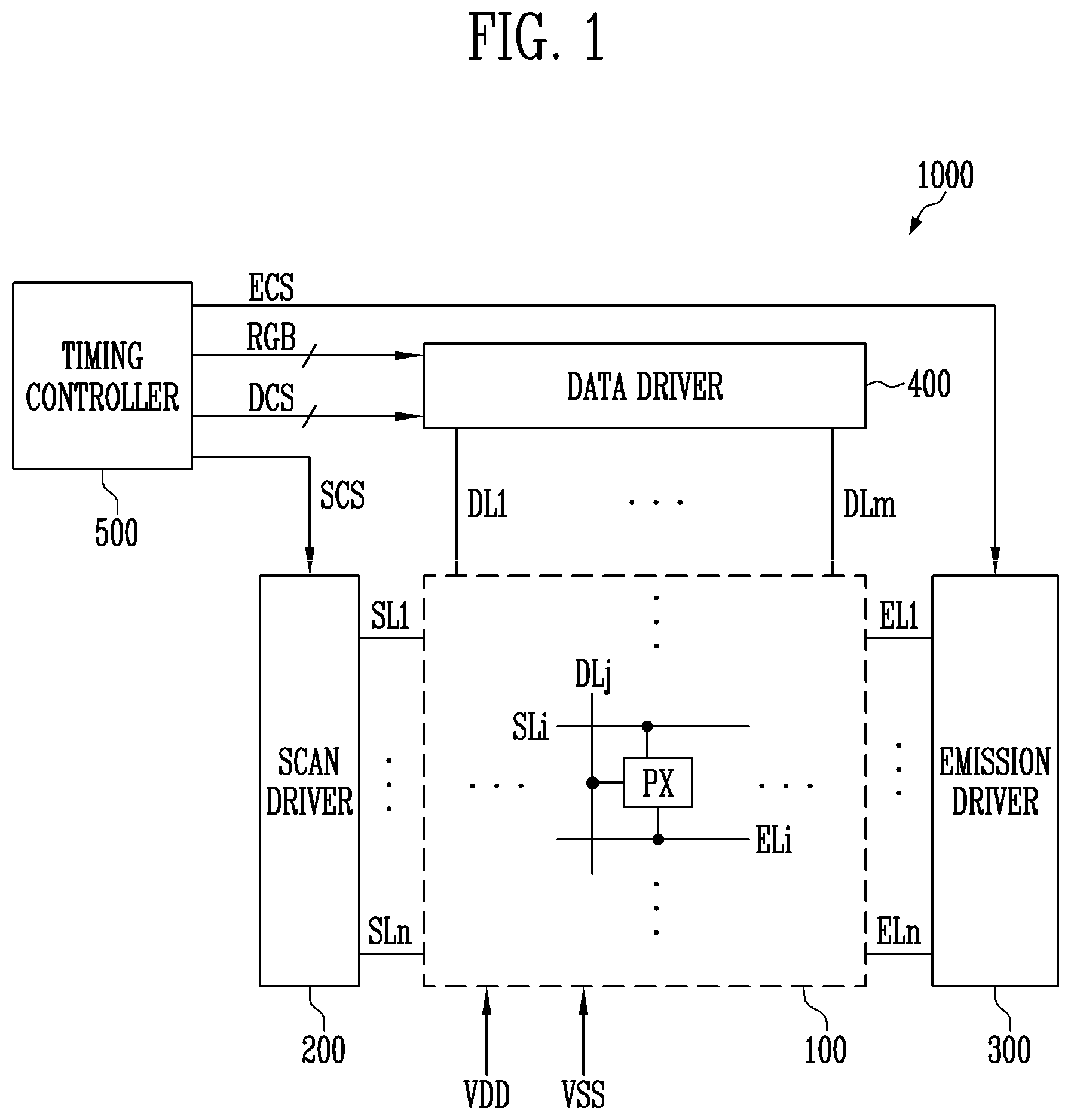
Referring to , the display device 1000 may include a pixel unit 100 (or display panel), a scan driver 200 (or first gate driver), an emission driver 300 (or second gate driver), a data driver 400 , and a timing controller 500 .
Hereinafter, it may be understood that the scan driver 200 and the emission driver 300 are one configuration of a gate driver.
The display device 1000 may display an image at various driving frequencies (or image refresh rates, or screen refresh rates) according to driving conditions. The driving frequency is a frequency at which a data voltage is substantially written to a driving transistor of a pixel PX. For example, the driving frequency is also referred to as a screen scan rate or a screen refresh frequency, and represents a frequency at which a display screen is refreshed for one second. The display device 1000 may display an image, corresponding to various driving frequencies.
In an embodiment, an output frequency of the data driver 400 with respect to one horizontal line (or pixel row) or an output frequency of the scan driver 200 outputting a scan signal may be determined corresponding to an image refresh rate. For example, a refresh rate for moving image driving may be a frequency of about 60 Hz or higher (e.g., 80 Hz, 96 Hz, 120 Hz, 240 Hz, or the like).
In an embodiment, the display device 1000 may adjust an output frequency of the scan driver 200 with respect to one horizontal line (or pixel row) and an output frequency of the data driver 400 , which corresponds to the output frequency of the scan driver 200 , according to driving conditions. For example, the display device 1000 may display an image, corresponding to various image refresh rates of 1 Hz to 240 Hz. However, this is merely illustrative, and the display device 1000 may also display an image at an image refresh rate of 240 Hz or higher (e.g., 480 Hz).
The pixel unit 100 may display an image. The pixel unit 100 may include pixels PX located to be connected to data lines DL 1 to DLm, scan lines SL 1 to SLn, and emission control lines EL 1 to ELn. The pixel PX may be supplied with voltages of a first driving power source VDD, a second driving power source VSS, and an initialization power source from the outside.
Additionally, each of the pixels PX may be connected to at least one scan line SLi and at least one emission control line ELi, corresponding to a pixel circuit structure. The pixel PX may include a driving transistor, a plurality of switching transistor implemented with at least one of an n-type transistor and a p-type transistor, and a light emitting element.
The timing controller 500 may receive an input control signal and an input image signal from an image source such as an external graphic device. The timing controller 500 may generate image data RGB suitable for an operation condition of the pixel unit 100 , based on the input image signal, and provide the image data RGB to the data driver 400 . The timing controller 500 may generate a first control signal SCS for controlling a driving timing of the scan driver 200 , a second control signal ECS for controlling a driving timing of the emission driver 300 , and a third control signal DCS for controlling a driving timing of the data driver 400 , based on the input control signal, and provide the first control signal SCS, the second control signal ECS, and the third control signal DCS respectively to the scan driver 200 , the emission driver 300 , and the data driver 400 .
The scan driver 200 may receive the first control signal SCS from the timing controller 500 . The scan driver 200 may supply a scan signal to the scan lines SL 1 to SLn in response to the first control signal SCS. The first control signal SCS may include a start pulse for the scan signal and a plurality of clock signals.
In an embodiment, the scan driver 200 may supply a scan signal to the scan lines SL 1 to SLn at the same frequency (e.g., a second frequency) as an image refresh rate of the display device 1000 . The scan signal may be a scan signal for writing a data signal to the driving transistor of the pixel PX. The second frequency may be set to an aliquot of a first frequency at which the emission driver 300 is driven.
The scan driver 200 may supply a scan signal having a pulse of a gate-on level to the scan lines SL 1 to SLn in a display scan period of one frame. In an example, the scan driver 200 may supply at least one scan signal to each of the scan lines SL 1 to SLn during the display scan period.
Also, the scan driver 200 may supply a scan signal maintained at a gate-off level to the scan lines SL 1 to SLn in a self-scan period of the one frame.
Meanwhile, the present disclosure is not limited thereto. For example, the scan driver 200 may additionally supply a scan signal for initialization or compensation to the pixels PX.
The emission driver 300 may receive the second control signal ECS from the timing controller 500 . The emission driver 300 an emission control signal to the emission control lines EL 1 to ELn in response to the second control signal ECS. The second control signal ECS may include a start pulse for the emission control signal and a plurality of clock signals.
In an embodiment, the emission driver 300 may supply the emission control signal to the emission control lines EL 1 to ELn at the first frequency. For example, the emission driver 300 may always supply an emission control signal to the emission control lines EL 1 to ELn at a constant frequency (e.g., the first frequency), regardless of the frequency of an image refresh rate. Therefore, in the one frame, emission control signals supplied to the emission control lines EL 1 to ELn may be repeatedly supplied for every predetermined cycle.
In addition, the first frequency may be set higher than the second frequency. In an embodiment, the frequency (or the second frequency) of the image refresh rate may be set to an aliquot of the first frequency.
For example, at all driving frequencies at which the display device 1000 can be driven, the emission driver 300 may perform scanning once during the display scan period, and perform scanning at least once according to the image refresh rate during the self-scan period.
That is, during the display scan period, an emission control signal may be sequentially output once to each of the emission control signals EL 1 to ELn. During the self-scan period, an emission control signal may be sequentially output at least once to each of the emission control signals EL 1 to ELn.
Accordingly, when the image refresh rate is decreased, a number of times the emission driver 300 repeatedly supplies an emission control signal to each of the emission control lines EL 1 to ELn in the one frame may be increased.
The data driver 400 may receive the third control signal DCS from the timing controller 500 . The data driver 400 may convert the image data RGB into an analog data signal (e.g., a data voltage) in response to the third control signal DCS, and supply the data signal to the data lines DL 1 to DLm.
Meanwhile, for convenience of description, a case where each of the scan driver 200 and the emission driver 300 is a single component has been illustrated in , but the present disclosure is not limited thereto. The scan driver 200 may include a plurality of scan drivers each of which supplies at least one of scan signals having different waveforms according to a design. In addition, at least a portion of the scan driver 200 and the emission driver 300 may be integrated as one driving circuit, one module, or the like.
In an embodiment, the display device 1000 may further include a power supply. The power supply may supply, to the pixel unit 100 , the voltage of the first power source VDD and the supply of the second driving power source VSS, which are used for driving of the pixel PX.
is a block diagram illustrating a scan driver (gate driver) in accordance with embodiments of the present disclosure.
Meanwhile, for convenience of description, four stages ST 1 to ST 4 included in the scan driver 200 and scan signals (or output signals OUT 1 to OUT 4 ) output therefrom.
In addition, the scan driver 200 is an example of a gate driver, and may be replaced with the emission driver 300 shown in .
Referring to , the scan driver 200 may include a plurality of stages ST 1 to ST 4 . The stages ST 1 to ST 4 may be respectively connected to corresponding scan lines SL 1 to SL 4 , and output a scan signal, corresponding to clock signals CLK 1 and CLK 2 .
A second stage ST 2 may be dependently connected to a first stage ST 1 , a third stage ST 3 may be dependently connected to the second stage ST 2 , and a fourth stage ST 4 may be dependently connected to the third stage ST 3 . The first to fourth stages ST 1 to ST 4 may have the substantially same configuration.
Each of the stages ST 1 to ST 4 may include a first input terminal 201 , a second input terminal 202 , a third input terminal 203 , a first power input terminal 204 , a second power input terminal 205 , a third power input terminal 206 , a first output terminal 207 , and a second output terminal 208 .
A first input terminal 201 of the first stage ST 1 may receive a start pulse SSP. In addition, each of first input terminals 201 of the second to fourth stages ST 2 to ST 4 may receive a carry signal (i.e., one of first to third carry signals CR 1 to CR 3 ) output from a second output terminal 208 of a previous stage. For example, the first input terminal 201 of the second stage ST 2 may receive the first carry signal CR 1 output from a second output terminal 208 of the first stage ST 1 , the first input terminal 201 of the third stage ST 3 may receive the second carry signal CR 2 output from a second output terminal 208 of the second stage ST 2 , and the first input terminal 201 of the fourth stage ST 4 may receive the third carry signal CR 3 output from a second output terminal 208 of the third stage ST 3 .
The first clock signal CLK 1 and the second clock signal CLK 2 may be alternately provided to second input terminals 202 and third input terminals 203 of the stages ST 1 to ST 4 .
In an embodiment, a second input terminal 202 of a kth (k is an integer greater than 0) stage may receive the first clock signal CLK 1 , and a third input terminal 203 of the kth stage may receive the second clock signal CLK 2 . On the other hand, a second input terminal 202 of a (k+1)th stage may receive the second clock signal CLK 2 , and a third input terminal 203 of the (k+1)th stage may receive the first clock signal CLK 1 .
For example, each of the second input terminals 202 of the first stage ST 1 and the third stage ST 3 may receive the first clock signal CLK 1 , and each of the third input terminals 203 of the first stage ST 1 and the third stage ST 3 may receive the second clock signal CLK 2 . In addition, each of the second input terminals of the second stage ST 2 and the fourth stage ST 4 may receive the second clock signal CLK 2 , and each of the third input terminals 203 of the second stage ST 2 and the fourth stage ST 4 may receive the first clock signal CLK 1 .
The first clock signal CLK 1 and the second clock signal CLK 2 may have the same cycle, and have waveforms of which phases do not overlap with each other. In an example, the second clock signal CLK 2 may be set as a signal shifted by about a half cycle from the first clock signal CLK 1 .
Voltages of power sources necessary for driving of the stages ST 1 to ST 4 may be applied to first to third power input terminals 204 , 205 , and 206 of the stages ST 1 to ST 4 .
For example, a voltage of a first power source VGH may be applied to a first power input terminal 204 of each of the stages ST 1 to ST 4 , and a voltage of a second power source VGL may be applied to a second power input terminal 205 of each of the stages ST 1 to ST 4 . Each of the voltage of the first power source VGH and the voltage of the second power source VGL may have a DC voltage level. A voltage level of the first power source VGH may be set higher than a voltage level of the second power source VGL.
In addition, a voltage of a third power source VREF may be applied to a third power input terminal 206 of each of the stages ST 1 to ST 4 . A voltage level of the third power source VREF may be lower than the voltage level of the first power source VGH and be higher than the voltage level of the second power source VGL. That is, the third power source VREF may have a voltage level between the first power source VGH and the second power source VGL.
Output signals OUT 1 to OUT 4 may be output to first output terminals 207 of the respective stages ST 1 to ST 4 . In an embodiment, the output signals OUT 1 to OUT 4 output to the first output terminals 207 are scan signals, and may be provided to corresponding scan lines SL 1 to SL 4 .
Carry signals CR 1 to CR 4 may be output to second output terminals 208 of the respective stages ST 1 to ST 4 . As described above, each of the carry signals CR 1 to CR 4 output to the second output terminals 208 may be provided to an input terminal 201 of a next stage. For example, the first carry signal CR 1 output from a second output terminal 208 of the first stage ST 1 may be provided to the first input terminal 201 of the second stage ST 2 , the second carry signal CR 2 output from a second output terminal 208 of the second stage ST 2 may be provided to the first input terminal 201 of the third stage ST 3 , the third carry signal CR 3 output from a second output terminal 208 of the third stage ST 3 may be provided to the first input terminal 201 of the fourth stage ST 4 , and a fourth carry signal CR 2 output from a second output terminal 208 of the fourth stage ST 4 may be provided to a first input terminal of a fifth stage.
In an embodiment, the stages ST 1 to ST 4 included in the scan driver 200 may have the substantially same configuration, except kinds of signals received through the first input terminals 201 of the stages ST 1 to ST 4 . For example, the first stage as an initial stage, which receives the start pulse SSP through the first input terminal 201 , and the other stages (e.g., the second to fourth stages ST 2 to ST 4 ), each of which receives a carry signal of a previous stage through the first input terminal 201 , may have the substantially same circuit configuration, except an input signal (i.e., the start pulse SSP or a carry signal of a previous stage) received through the first input terminal 201 , and operate substantially identical to each other.
Accordingly, hereinafter, for convenience description, the stages included in the scan driver 200 will be described based on the first stage ST 1 .
is a circuit diagram illustrating an example of the first stage included in the scan driver shown in .
Referring to , the first stage ST 1 may include a first sub-stage circuit LB 1 .
The first sub-stage circuit LB 1 may generate and output a first output signal OUT 1 and the first carry signal CR 1 , based on an input signal (e.g., the start pulse SSP), the first clock signal CLK 1 , the second clock signal CLK 2 , the voltage of the first power source VGH, and the voltage of the second power source VGL.
In an embodiment, the first sub-stage circuit LB 1 may include a first driver SST 1 , a second driver SST 2 , and an output unit SST 3 .
The first driver SST 1 may receive the input signal (e.g., the start pulse SSP) through the first input terminal 201 , receive the first clock signal CLK 1 through the second input terminal 202 , and receive the second clock signal CLK 2 through a third input terminal 203 . Also, the first driver SST 1 may be connected to the first power source VGH through a first power input terminal 204 , and be connected to the second power source VGL through a second power input terminal 205 .
The first driver SST 1 may control voltages of a first node Q and a second node QB, based on the start pulse SSP, the first clock signal CLK 1 , the second clock signal CLK 2 , the first power source VGH, and the second power source VGL.
To this end, the first driver SST 1 may include first to sixth transistors T 1 to T 6 and a first capacitor C 1 .
The first transistor T 1 may be connected between the first input terminal 201 and an input node NI, and include a gate electrode connected to the second input terminal 202 . The first transistor T 1 may be turned on when the first clock signal CLK 1 supplied through the second input terminal 202 has a gate-on level (e.g., a low level), to electrically connect the first input terminal 201 and the input node NI to each other.
In an embodiment, the first transistor T 1 may include a plurality of sub-transistors connected in series to each other. This will be described in detail with reference to .
The second transistor T 2 may include a first electrode connected to the first power input terminal 204 and a gate electrode connected to the second node QB. The second transistor T 2 may be turned on or turned off based on the voltage of the second node QB.
The third transistor T 3 may be connected between a second electrode of the second transistor T 2 and the input node NI, and include a gate electrode connected to the third input terminal 203 . The third transistor T 3 may be turned on when the second clock signal CLK 2 supplied through the third input terminal 203 has the gate-on level (e.g., the low level), to electrically connect the second transistor T 2 (e.g., the second electrode of the second transistor T 2 ) and the input node NI to each other.
The fourth transistor T 4 may be connected between the second node QB and the second input terminal 202 , and include a gate electrode connected to the input node NI. The fourth transistor T 4 may be turned on or turned off based on a voltage of the input node NI.
The fifth transistor T 5 may be connected between the second node QB and the second power input terminal 205 , and include a gate electrode connected to the second input terminal 202 . The fifth transistor T 5 may be turned on when the first clock signal CLK 1 supplied through the second input terminal 202 has the gate-on level (e.g., the low level), to electrically connect the second node QB and the second power input terminal 205 to each other.
The sixth transistor T 6 may be connected between the input node NI and the first node Q, and include a gate electrode connected to the second power input terminal 205 . Since the voltage of the second power source VGL, which have the low level (or the gate-on level), is supplied to the gate electrode of the sixth transistor T 6 through the second power input terminal 205 , the sixth transistor T 6 can always maintain a turn-on state. Thus, the voltage of the input node NI does not become lower than the voltage of the second power source VGL, so that bias stress which may be applied to the first transistor T 1 can be reduced. For example, the voltage of the input node N 1 may be equal to or greater than a sum of absolute values of the voltage of the second power source VGL and a threshold voltage of the sixth transistor T 6 .
The first capacitor C 1 may be connected between the first power input terminal 204 and the second node QB. For example, the first capacitor C 1 may include a first electrode connected to the first power input terminal 204 and a second electrode connected to the second node QB. Since one electrode of the first capacitor C 1 is connected to the first power input terminal 204 to which the voltage of the first power source VGH is supplied, the first capacitor C 1 charges a voltage applied to the second node QB, and stably maintains the voltage of the second node QB.
The second driver SST 2 may be connected to the first node Q and the second node QB, receive the voltage of the first power source VGH through the first power input terminal 204 , and receive the second clock signal CLK 2 through the third input terminal 203 .
The second driver SST 2 may control a voltage of an output node QB_F, based on the voltage of the first node Q, the voltage of the second node QB, the voltage of the first power source VGH, and a signal level of the second clock signal CLK 2 . Also, the second driver SST 2 may out the first carry signal CR 1 through the second output terminal 208 , based on the voltage of the first node Q, the voltage of the second node QB, the voltage of the first power source VGH, and the signal level of the second clock signal CLK 2 . The first carry signal CR 1 may correspond to the voltage of the output node QB_F, and a signal corresponding to a voltage level of the output node QB_F may be output as the first carry signal. For example, the voltage of the first power source VGH may correspond to a high level of the first carry signal CR 1 , and a low level of the second clock signal CLK 2 may correspond to a low level of the first carry signal CR 1 . Meanwhile, as described with reference to , the first carry signal CR 1 may be provided to a next stage (e.g., the second stage ST 2 shown in ).
To this end, the second driver SST 2 may include a seventh transistor T 7 , an eighth transistor T 8 , and a second capacitor C 2 .
The seventh transistor T 7 may be connected between the first power input terminal 204 and the output node QB_F, and include a gate electrode connected to the second node QB. The seventh transistor T 7 may be turned on or turned off based on the voltage of the second node QB. When the seventh transistor T 7 is turned on, the voltage of the first power source VGH, which has a high level, may be supplied to the output node QB_F.
The eighth transistor T 8 may be connected between the third input terminal 203 and the output node QB_F, and include a gate electrode connected to the first node Q. The eighth transistor T 8 may be turned on or turned off based on the voltage of the first node Q. When the eighth transistor T 8 is turned on, the second clock signal CLK 2 may be supplied to the output node QB_F.
As described above, the voltage of the output node QB_F may be controlled according to the turn-on or turn-off of the seventh and eighth transistors T 7 and T 8 .
The second capacitor C 2 may be connected between the first node Q 1 and the output node QB_F. For example, the second capacitor C 2 may include a first electrode connected to the first node Q and a second electrode connected to the output node QB_F.
The output unit SST 3 may be connected to the output node QB_F. The output unit SST 3 may receive the voltage of the first power source VGH through the first power input terminal 204 and receive the voltage of the second power source VGL through the second power input terminal 205 .
The output unit SST 3 may output the first output signal OUT 1 , based on the voltage of the output node QB_F, the voltage of the first power source VGH, and the voltage of the second power source VGL. For example, the voltage of the first power source VGH may correspond to a high level of the first output signal OUT 1 , and the voltage of the second power source VGL may correspond to a low level of the first output signal OUT 1 . The first output signal OUT 1 is a scan signal, and may be provided to a first scan line SL 1 through a first output terminal 207 .
To this end, the output unit SST 3 may include a ninth transistor T 9 and a tenth transistor T 10 .
The ninth transistor T 9 may be connected between the first power input terminal 204 and the first output terminal 207 , and include a gate electrode connected to the output node QB_F. The ninth transistor T 9 may be turned on or turned off based on the voltage of the output node QB_F. When the ninth transistor T 9 is turned on, the first output signal OUT 1 supplied to the first output terminal 207 may have a high level (e.g., a gate-on voltage level of an n-type transistor).
The tenth transistor T 10 may be connected between the second power input terminal 205 and the first output terminal 207 , and include a gate electrode connected to the output node QB_F. The tenth transistor T 10 may be turned on or turned off based on the voltage of the output node QB_F. When the tenth transistor T 10 is turned on, the first output signal OUT 1 supplied to the first output terminal 207 may have a low level (e.g., a gate-off voltage level of the n-type transistor).
In an embodiment, the output unit SST 3 of the first sub-stage circuit LB 1 may be implemented as a complementary metal oxide silicon (COMS) circuit (hereinafter, referred to as a CMOS circuit).
For example, the ninth transistor T 9 of the output unit SST 3 may be implemented as a p-type transistor, and the tenth transistor T 10 of the output unit SST 3 may be implemented as an n-type transistor. Since the gate electrode of the ninth transistor T 9 and the gate electrode of the tenth transistor T 10 are commonly connected to the output node QB_F, the tenth transistor T 10 may be turned off when the ninth transistor T 9 is turned on corresponding to the voltage of the output node QB_F, and be turned on when the ninth transistor T 9 is turned off corresponding to the voltage of the output node QB_F. Accordingly, the first output signal OUT 1 output through the first output terminal 207 may have a voltage level of the first power source VGH, which is the high level, or a voltage level of the second power source VGL, which is the low level.
The output unit SST 3 of the first sub-stage circuit LB 1 is implemented as the CMOS circuit, so that the p-type transistor (e.g., the ninth transistor T 9 ) takes charge of and performs a pull-up function and the n-type transistor (e.g., the tenth transistor T 1 ) takes charge of and performs a pull-down function. Thus, the current driving ability of the first sub-stage circuit LB 1 (or the first stage ST 1 ) in accordance with the embodiments of the present disclosure can be relatively improved as compared with the existing stage circuit configured with only p-type transistors or n-type transistors.
As described above, the first sub-stage circuit LB 1 includes the first driver SST 1 , the second driver SST 2 , and the output unit SST 3 , so that the first stage ST 1 takes charge of and performs a function of outputting the first output signal OUT 1 (or a first scan signal) through the first scan line SL 1 . An operation and an effect of the first sub-stage circuit LB 1 will be described in detail with reference to .
Meanwhile, as described with reference to , stages (e.g., the stages ST 1 to ST 4 shown in ) of a scan driver (e.g., the scan driver 200 shown in ) are substantially identical or similar to one another, except a signal received through a first input terminal 201 of each of the stages. Therefore, the other stages (e.g., the second to fourth stages ST 2 to ST 4 shown in ) of the scan driver (e.g., the scan driver 200 shown in ) except the first stage ST 1 may have the substantially same circuit configuration as the first stage ST 1 and operate substantially identical to the first stage ST 1 , except that each of the other stages receives a carry signal of a previous stage through the first input terminal 201 .
Meanwhile, as described above, since the output unit SST 3 of the first sub-stage circuit LB 1 is implemented as the CMOS circuit, the output unit SST 3 includes an n-type transistor (e.g., the tenth transistor T 10 ). A channel of the tenth transistor T 10 implemented as the n-type transistor may be implemented with an oxide semiconductor. The oxide semiconductor may have a negative threshold voltage according to the kind thereof. Therefore, it is necessary to set the tenth transistor T 10 to have a positive threshold voltage by applying a voltage (e.g., a bias voltage Vbias) lower than the voltage of the second power source VGL to the tenth transistor T 10 (e.g., a back-gate electrode of the tenth transistor T 10 ).
To this end, the first stage ST 1 in accordance with the embodiments of the present disclosure may further include a first charge pump circuit CPB 1 for applying the bias voltage Vbias to the n-type transistor included in the output unit SST 3 implemented as the CMOS circuit.
The first charge pump circuit CPB 1 may receive the second clock signal CLK 2 through the third input terminal 203 . Also, the first charge pump circuit CPB 1 may be connected to the second power source VGL through the second power input terminal 205 , and be connected to the third power source VREF through a third power input terminal 206 .
In an embodiment, the first charge pump circuit CPB 1 may generate the bias voltage Vbias, based on the second clock signal CLK 2 , the voltage of the second power source VGL, and the voltage of the third power source VREF, and supply the bias voltage Vbias to the output unit SST 3 (or the tenth transistor T 10 of the output unit SST 3 ).
To this end, the first charge pump circuit CPB 1 may include eleventh to thirteenth transistors T 11 to T 13 , a third capacitor C 3 , and a fourth capacitor C 4 .
The eleventh transistor T 11 may be connected between the third power input terminal 206 and a third node PPN, and include a gate electrode connected to the third power input terminal 206 . By the voltage of the third power source VREF supplied through the third power input terminal 206 , the eleventh transistor T 11 may be turned, to supply the voltage of the third power source VREF to the third node PPN.
The twelfth transistor T 12 may include a first electrode connected to the third input terminal 203 and a gate electrode connected to the third node PPN. The twelfth transistor T 12 may be turned on or turned off based on a voltage of the third node PPN. For example, the twelfth transistor T 12 may be turned on based on the voltage of the third node PPN, which has a voltage level lower equal to or lower than the voltage level of the third power source VREF.
The third capacitor C 3 may be connected between a second electrode of the twelfth transistor T 12 and the third node PPN. For example, the third capacitor C 3 may include a first electrode connected to the second electrode of the twelfth transistor T 12 and a second electrode connected to the third node PPN. The third capacitor C 3 may store a voltage difference between the second electrode of the twelfth transistor T 12 and the third node PPN. Accordingly, a change in voltage supplied to the second electrode of the twelfth transistor T 12 (or the first electrode of the third capacitor C 3 ) can be reflected to the third node PPN (or the second electrode of the third capacitor C 3 ).
The thirteenth transistor T 13 may be connected between the third node PPN and the output unit SST 3 (e.g., the back-gate electrode of the tenth transistor T 10 ). For example, the thirteenth transistor T 13 may include a first electrode connected to the third node PPN and a second electrode connected to the back-gate electrode of the tenth transistor T 10 . The thirteenth transistor T 13 may include a gate electrode connected to the third node PPN. The thirteenth transistor T 13 may be turned on or turned off based on the voltage of the third node PPN.
The fourth capacitor C 4 may be connected between the second power input terminal 205 and the second electrode of the thirteenth transistor T 13 . For example, the fourth capacitor C 4 may include a first electrode connected to the second power input terminal 205 and a second electrode connected to the second electrode of the thirteenth transistor T 13 .
In an embodiment, the fourth capacitor C 4 may store a voltage difference between the second power input terminal 205 and the second electrode of the thirteenth transistor T 13 . Since the voltage of the second power source VGL as a constant voltage is supplied to the second power input terminal 205 , a voltage, i.e., the bias voltage Vbias of the second electrode of the thirteenth transistor T 13 can be stably maintained by the fourth capacitor C 4 .
Meanwhile, when a parasitic capacitance with respect to the bias voltage Vbias is sufficient according to a circuit layout of the first stage ST 1 , the fourth capacitor C 4 may be omitted from the first charge pump circuit CPB 1 .
In an embodiment, by using the voltage of the third power source VREF, which has a voltage level between the first power source VGH and the second power source VGL, the first charge pump circuit CPB 1 may generate the bias voltage Vbias lower than the voltage level of the second power source VGL and supply the bias voltage Vbias to the back-gate electrode of the tenth transistor T 10 included in the output unit SST 3 .
For example, when the signal level of the second clock signal CLK 2 is changed from a high level to a low level, the voltage of the third node PPN becomes lower by a difference between the high level and the low level of the second clock signal CLK 2 from the existing voltage level (e.g., the voltage of the third power source VREF) due to coupling of the third capacitor C 3 . Accordingly, the voltage of the third node PPN has a voltage level lower than the voltage level of the second power source VGL, which is the low level. Thus, the voltage of the third node PPN, which is lower than the voltage level of the second power source VGL, is supplied as the bias voltage Vbias to the tenth transistor T 10 of the output unit SST 3 through the thirteenth transistor T 13 .
Meanwhile, as described above, in order to change a threshold voltage of the tenth transistor T 10 by supplying the bias voltage Vbias to the back-gate electrode of the tenth transistor T 10 as the n-type transistor included in the output unit SST 3 implemented as the CMOS circuit, it is necessary for the bias voltage Vbias to have a voltage level lower than the voltage level of the second power source VGL. When the scan driver 200 (or the display device 1000 ) includes a separate voltage source for supplying the bias voltage Vbias, a separate voltage source in addition to the first power source VGH and the second power source VGL, which are necessary for driving of the stages of the scan driver 200 , is added, and therefore, it can be disadvantageous in terms of power consumption.
On the other hand, the scan driver 200 (or the first stage ST 1 ) in accordance with the embodiments of the present disclosure includes a charge pump circuit (e.g., the first charge pump circuit CPB 1 ), so that the bias voltage Vbias having a voltage level lower than the voltage level of the second power source VGL can be generated by using the third power source VREF. Since the third power source VREF has a voltage level between the first power source VGH and the second power source VGL, the display device ( 1000 shown in ) (or the power supply included in the display device 1000 ) can generate the voltage of the third power source VREF by changing the voltages of the first power source VGH and the second power source VGL through a voltage regulator circuit. Since the voltage regulator circuit is configured as a relatively simple circuit, the display device ( 1000 shown in ) can be simplified and be advantageous in terms of power consumption, as compared with the case where the display device ( 1000 shown in ) includes the separate voltage source.
Hereinafter, operations of the first sub-stage circuit LB 1 and the first charge pump circuit CPB 1 of the first stage ST 1 will be described in detail with reference to .
is a timing diagram illustrating an example of driving of the first stage shown in .
Referring to to 4 , the first clock signal CLK 1 and the second clock signal CLK 2 may be supplied at different timings. For example, the second clock signal CLK 2 may be set as a signal shifted by a half cycle (e.g., one horizontal period) from the first clock signal CLK 1 . In an example, the first clock signal CLK 1 having a low level L may be supplied through the second input terminal 202 at a first time t 1 , and the second clock signal CLK 2 having the low level L may be supplied through the third input terminal 203 at a second time t 2 after the first time t 1 .
Meanwhile, a high level H (or high voltage) shown in may correspond to the voltage of the first power source VGH, and the low level L (or low voltage) shown in may correspond to the voltage of the second power source VGL. For example, the voltage of the first power source VGH may be a positive voltage, and the voltage of the second power source VGL may be a negative voltage. However, this is merely illustrative, and the high level H and the low level L are not limited thereto. For example, a voltage having the high level H and a voltage having the low level L may be set according to a kind of transistor, a use environment of the display device, and the like.
Meanwhile, a 2-low level 2L may correspond to a voltage level corresponding to two times of the low level L.
The start pulse SSP may have the high level H at the first time t 1 , the second time t 2 , and an eighth time t 8 . The start pulse SSP may have the low level L at third to seventh times t 3 to t 7 .
As described with reference to , the eleventh transistor T 11 is turned on by the voltage of the third power source VREF supplied through the third power input terminal 206 , and therefore, the voltage of the third power source VREF may be supplied to the third node PPN.
Meanwhile, the second clock signal CLK 2 supplied through the third input terminal 203 at the first time t 1 may have the high level H. As the twelfth transistor T 12 is turned on by the voltage of the third node PPN, a voltage having the high level H may be supplied to the second electrode of the twelfth transistor T 12 (or the first electrode of the third capacitor C 3 ). Accordingly, the third capacitor C 3 may store a voltage corresponding to a difference between the voltage having the high level H and the voltage of the third power source VREF.
Subsequently, at the second time t 2 , the second clock signal CLK 2 having the low level L may be applied through the third input terminal 203 . Accordingly, the voltage of the second electrode of the twelfth transistor T 12 (or the first electrode of the third capacitor C 3 ) is changed from the existing voltage having the high level H to a voltage having the low level L, and the voltage of the third node PPN becomes lower by a voltage variation of the first electrode of the third capacitor C 3 (i.e., a difference between the voltage having the high level H and the voltage having the low level L) from the existing voltage level of the third power source VREF due to coupling of the third capacitor C 3 . The bias voltage Vbias having a voltage level lower than the voltage of the second power source VGL may be supplied to the output unit SST 3 (e.g., the tenth transistor T 10 ) of the first sub-stage circuit LB 1 by the thirteenth transistor T 13 turned on by the voltage of the third node PPN. Charges existing in the back-gate electrode of the tenth transistor T 10 come out through the turned-on thirteenth transistor T 13 , and accordingly, the tenth transistor T 10 implemented as the n-type transistor may be set to have a positive threshold voltage.
Meanwhile, since the first electrode of the fourth capacitor C 4 is connected to the second power input terminal 205 to which the voltage of the second power source VGL as a constant voltage is supplied, the bias voltage Vbias corresponding to the second electrode of the fourth capacitor C 4 can be stably maintained.
While such a process (e.g., a charge pumping process) is repeated, the stabilized bias voltage Vbias becomes lower than the voltage having the low level L (e.g., the voltage of the second power source VGL). Thus, in accordance with the embodiments of the present disclosure, it is unnecessary for the display device ( 1000 shown in ) to include a separate voltage source. Hence, the display device ( 1000 shown in ) is simplified, and it can be disadvantageous in terms of power consumption.
Hereinafter, a configuration in which the first stage ST 1 supplies the first output signal OUT 1 (or the first scan signal) through the first scan line SL 1 will be described through an operation of the first sub-stage circuit LB 1 at the third to eighth times t 3 to t 8 .
At the third time t 3 , the start pulse SSP having the low level L may be supplied through the first input terminal 201 . The start pulse SSP supplied to the first input terminal 201 may have the low level L until before the eighth time t 8 (e.g., until an arbitrary time between the seventh time t 7 and the eighth time t 8 ) from the third time t 3 .
Subsequently, at the fourth time t 4 , the first clock signal CLK 1 having the low level L (or gate-on level) may be supplied through the second input terminal 202 , so that the first transistor T 1 and the fifth transistor T 5 are turned on.
When the first transistor T 1 is turned on, the low level L of the start pulse SSP may be supplied to the input node NI. Meanwhile, since the gate electrode of the sixth transistor T 6 is connected to the second power input terminal 205 to always maintain the turn-on state, the low level L of the start pulse SSP may be supplied to the first node Q. Accordingly, the voltage of the first node Q may be changed to the low level L.
In addition, when the fifth transistor T 5 is turned on, the second power source VGL having the low level is supplied to the second node QB, and accordingly, the voltage of the second node QB maintains the low level L.
Subsequently, at the fifth time, the first clock signal CLK 1 supplied to the second input terminal 202 may be changed from the low level L to the high level H. Accordingly, the first transistor T 1 and the fifth transistor T 5 may be turned off.
Meanwhile, since the voltage of the input node N 1 is maintained at the low level L, the fourth transistor T 4 may be in the turn-on state. Accordingly, the high level H of the first clock signal CLK 1 may be supplied to the second node QB, so that the voltage of the second node QB is changed to the high level H.
Subsequently, at the sixth time t 6 , the second clock signal CLK 2 having the low level L (or gate-on level) may be supplied through the third input terminal 203 , so that the third transistor T 3 is turned on.
Meanwhile, the eighth transistor T 8 may maintain the turn-on state, based on the voltage of the first node Q, which has the low level L (or gate-on level). The low level L of the second clock signal CLK 2 may be supplied to the output node QB_F through the eighth transistor T 8 , so that the voltage of the output node QB_F is changed from the existing high level H to the low level L. The voltage of the first node Q decreases from the low level L to the 2-low level 2L due to coupling of the second capacitor C 2 , and the eighth transistor T 8 stably maintains the turn-on state.
In addition, based on the voltage of the output node QB_F, which has the low level L, the ninth transistor T 9 of the output unit SST 3 may be turned on and the tenth transistor T 10 of the output unit SST 3 may be turned off. Accordingly, the voltage of the first power source VGH, which have the high level H, is supplied to the first output terminal 207 , so that the first output signal OUT 1 can be output at the high level H.
Meanwhile, the first carry signal CR 1 may be output at the low level L, corresponding to the voltage of the output node QB_F, which has the low level L.
Subsequently, at the seventh time t 7 , the second clock signal CLK 2 supplied to the third input terminal 203 may be changed from the low level L to the high level H. The high level H of the second clock signal CLK 2 may be supplied to the output node QB_F through the eighth transistor T 8 in the turn-on state. Accordingly, based on the voltage of the output node QB_F, which has the high level H, the ninth transistor T 9 of the output unit SST 3 may be turned off and the tenth transistor T 10 of the output unit SST 3 may be turned on, so that the first output signal OUT 1 having the low level L is output.
Meanwhile, the first carry signal CR 1 may be output at the high level H, corresponding to the voltage of the output node QB_F, which has the high level H.
After the seventh time t 7 , the start pulse SSP may be changed from the low level L to the high level H.
At the eighth time t 8 , the first clock signal CLK 1 having the low level L (or gate-on level) may be supplied through the second input terminal 202 , so that the first transistor T 1 and the fifth transistor T 5 are turned on.
However, unlike the start pulse SSP at the fourth time t 4 , the start pulse SSP has the high level H, and hence the high level H of the start pulse SSP may be supplied to the first node Q through the sixth transistor T 6 in the turn-on state. Therefore, the voltage of the first node Q may be changed to the high level H.
In addition, the voltage of the second power source VGL, which has the low level, may be supplied to the second node QB through the fifth transistor T 5 in the turn-on state, so that the second node QB is changed to the low level L.
Meanwhile, as described above, since the stages (ST 1 to ST 4 shown in ) included in the scan driver ( 200 shown in ) have the substantially same configuration, except input signals received through the first input terminals 201 thereof, the other stages (e.g., the second to fourth stages ST 2 to ST 4 shown in ) except the first stage ST 1 can output output signals (e.g., OUT 2 and OUT 3 ) to the scan lines through an operation substantially identical to an operation of the first stage ST 1 .
is a circuit diagram illustrating an example of the first stage included in the scan driver shown in . In , portions different from those of the above-described embodiment will be mainly described to avoid redundancy. Portions not particularly described in the embodiment shown in follow those of the above-described embodiment. In addition, identical reference numerals refer to identical components, and similar reference numerals refer to similar components.
A first stage ST 1 _ 1 shown in represents a modified embodiment of the first stage ST 1 described with reference to .
Referring to , the first stage ST 1 _ 1 shown in may include the first sub-stage circuit LB 1 and a first charge pump circuit CPB 1 _ 1 . Meanwhile, the first state ST 1 _ 1 shown in and the first stage ST 1 shown in are substantially identical or similar to each other, except a connection configuration of the eleventh transistor T 11 and that the first stage ST 1 _ 1 further includes a fourteenth transistor T 14 , and therefore, overlapping descriptions will not be repeated.
The first charge pump circuit CPB 1 _ 1 of the first stage ST 1 _ 1 may receive the first clock signal CLK 1 through the second input terminal 202 , and receive the second clock signal CLK 2 through the third input terminal 203 . Also, the first charge pump circuit CPB_ 1 may be connected to the second power source VGL through the second power input terminal 205 , and be connected to the third power source VREF through the third power input terminal 206 .
In an embodiment, the first charge pump circuit CPB 1 _ 1 may generate a bias voltage Vbias, based on the first clock signal CLK 1 , the second clock signal CLK 2 , the voltage of the second power source VGL, and the voltage of the third power source VREF, and supply the bias voltage Vbias to the output unit SST 3 (or the tenth transistor T 10 of the output unit SST 3 ).
To this end, the first charge pump circuit CPB 1 _ 1 may include eleventh to fourteenth transistors T 11 _ 1 , T 12 , T 13 , and T 14 , the third capacitor C 3 , and the fourth capacitor C 4 .
The fourteenth transistor T 14 may be connected between the third power input terminal 206 and the eleventh transistor T 11 _ 1 . For example, the fourteenth transistor T 14 may include a first electrode connected to the third power input terminal 206 and a second electrode connected to the eleventh transistor T 11 _ 1 . Also, the fourteenth transistor T 14 may include a gate electrode connected to the second input terminal 202 . The fourteenth transistor T 14 may be turned on or turned off based on a signal level of the first clock signal CLK 1 .
The eleventh transistor T 11 _ 1 may be connected between the second electrode of the fourteenth transistor T 14 and the third node PPN. The eleventh transistor T 11 _ 1 may include a gate electrode connected to the second power input terminal 205 . Since the voltage of the second power source VGL, which has the low level (or gate-on level), is supplied to the gate electrode of the eleventh transistor T 11 _ 1 through the second power input terminal 205 , the eleventh transistor T 11 _ 1 may always maintain the turn-on state. Accordingly, when the fourteenth transistor T 14 is turned on by receiving the first clock signal CLK 1 have the gate-on level (e.g., the low level), the voltage of the third power source VREF may be supplied to the third node PPN.
For example, further referring to , when the first clock signal CLK 1 having the low level L is supplied through the second input terminal 202 at the first time t 1 , the fourth transistor T 14 may be turned on based to the first clock signal CLK 1 .
The eleventh transistor T 11 _ 1 always maintains the turn-on state by the voltage of the second power source VGL supplied through the second power input terminal 205 , and therefore, the voltage of the third power source VREF may be supplied to the third node PPN at the first time t 1 .
is a circuit diagram illustrating an example of the first stage included in the scan driver shown in . In , portions different from those of the above-described embodiment will be mainly described to avoid redundancy. Portions not particularly described in the embodiment shown in follow those of the above-described embodiment. In addition, identical reference numerals refer to identical components, and similar reference numerals refer to similar components.
A first stage ST 1 _ 2 shown in represents a modified embodiment of the first stage ST 1 _ 1 described with reference to .
Referring to , the first stage ST 1 _ 2 shown in may include a first sub-stage circuit LB 1 _ 1 and a first charge pump circuit CPB 1 _ 2 .
In an embodiment, a first transistor T 1 _ 1 included in the first sub-stage circuit LB 1 _ 1 or a fourteenth transistor T 14 _ 1 included in the first charge pump circuit CPB 1 _ 2 may include a plurality of sub-transistors connected in series to each other.
For example, the first transistor T 1 _ 1 may include first and second sub-transistors T 1 a and T 1 b connected in series to each other. Each of the first and second sub-transistors T 1 a and T 1 b may include a gate electrode commonly connected to the second input terminal 202 (e.g., referred to as a dual gate structure). Accordingly, current leakage caused by the first transistor T 1 _ 1 can be minimized.
In another example, the fourteenth transistor T 14 _ 1 may include third and fourth sub-transistors T 14 a and T 14 b connected in series to each other. Each of the third and fourth sub-transistors T 14 a and T 14 b may include a gate electrode commonly connected to the second input terminal 202 . Accordingly, current leakage caused by the fourteenth transistor T 14 _ 1 can be minimized.
However, this is merely illustrative, and at least one of the other transistors in addition to the first transistor T 1 _ 1 and the fourteenth transistor T 14 _ 1 may have a dual gate structure.
is a circuit diagram illustrating an example of the first stage included in the scan driver shown in . is a circuit diagram illustrating an example of the first stage included in the scan driver shown in . In , portions different from those of the above-described embodiment will be mainly described to avoid redundancy. Portions not particularly described in the embodiment shown in follow those of the above-described embodiment. In addition, identical reference numerals refer to identical components, and similar reference numerals refer to similar components.
Each of first stages ST 1 _ 3 and ST 1 _ 4 shown in represents a modified embodiment of the first stage ST 1 _ 1 described with reference to .
Referring to , 7 , and 8 , the first stage ST 1 _ 3 shown in may include the first sub-stage circuit LB 1 and a first charge pump circuit CPB 1 _ 3 , and the first stage ST 1 _ 4 shown in may include the first sub-stage circuit LB 1 and a first charge pump circuit CPB 1 _ 4 .
As described with reference to to 5 , it is necessary for the first electrode of the fourth capacitor C 4 to be connected to a constant voltage such that the fourth capacitor C 4 included in the first charge pump circuit CPB 1 allows the bias voltage Vbias to be stably maintained.
For example, as shown in , a fourth capacitor C 4 _ 1 may be connected between the first power input terminal 204 and the second electrode of the thirteenth transistor T 13 . That is, a first electrode of the fourth capacitor C 4 _ 1 may be connected to the first power input terminal 204 to which the first power source VGH as a constant voltage is supplied.
In another example, as shown in , a fourth capacitor C 4 _ 2 may be connected between the third power input terminal 206 and the second electrode of the thirteenth transistor T 13 . That is, a first electrode of the fourth capacitor C 4 _ 2 may be connected to the third power input terminal 206 to which the third power source VREF as a constant voltage is supplied.
is a circuit diagram illustrating an example of the first stage included in the scan driver shown in . In , portions different from those of the above-described embodiment will be mainly described to avoid redundancy. Portions not particularly described in the embodiment shown in follow those of the above-described embodiment. In addition, identical reference numerals refer to identical components, and similar reference numerals refer to similar components.
A first stage ST 1 _ 5 shown in represents a modified embodiment of the first stage ST 1 _ 1 described with reference to .
Referring to , the first stage ST 1 _ 5 shown in may include the first sub-stage LB 1 and a first charge pump circuit CPB 1 _ 5 . Meanwhile, the first stage ST 1 _ 5 shown in and the first stage ST 1 _ 1 shown in are substantially identical or similar to each other, except that the first stage ST 1 _ 5 further includes a fifteenth transistor T 15 , and therefore, overlapping descriptions will not be repeated.
The first charge pump circuit CPB 1 _ 5 may include eleventh to fifteenth transistors T 11 _ 1 and T 12 to T 15 , the third capacitor C 3 , and the fourth capacitor C 4 .
The fifteenth transistor T 15 may be connected between the third node PPN and the thirteenth transistor T 13 (e.g., the first electrode of the thirteenth transistor T 13 ), and include a gate electrode connected to the third node PPN. Accordingly, the fifteenth transistor T 15 may operate substantially identical to the thirteenth transistor T 13 described with reference to .
is a block diagram illustrating a scan driver (gate driver) in accordance with embodiments of the present disclosure. In , portions different from those of the above-described embodiment will be mainly described to avoid redundancy. Portions not particularly described in the embodiment shown in follow those of the above-described embodiment. In addition, identical reference numerals refer to identical components, and similar reference numerals refer to similar components.
A scan driver 200 _ 1 shown in represents a modified embodiment of the scan driver 200 described with reference to .
Referring to , the scan driver 200 _ 1 shown in may include a plurality of sub-stage circuits LB 1 _ 2 to LB 4 _ 2 . The sub-stage circuits LB 1 _ 2 to LB 4 _ 2 may be substantially identical to a sub-stage circuit (e.g., the first sub-stage circuit LB 1 ) included in each of the stages ST 1 to ST 4 described with reference to .
For example, the sub-stage circuits LB 1 _ 2 to LB 4 _ 2 shown in may have the substantially same configuration, and be dependently connected to each other.
Also, each of the sub-stage circuits LB 1 _ 2 to LB 4 _ 2 may include a first input terminal 201 receiving an input signal (e.g., the start pulse SSP or a previous carry signal), a second input terminal 202 receiving the first clock signal CLK 1 , a third input terminal 203 receiving the second clock signal CLK 2 , a first power input terminal 204 to which the voltage of the first power source VGH is applied, and a second power input terminal 205 to which the voltage of the second power source VGL is applied.
Also, each of the sub-stage circuits LB 1 _ 2 to LB 4 _ 2 may include a first output terminal 207 and a second output terminal 208 . The output signals OUT 1 to OUT 4 may be output to first output terminals 207 of the respective sub-stage circuits LB 1 _ 2 to LB 4 _ 2 , and the carry signals CR 1 to CR 4 may be output to second output terminals 208 of the respective sub-stage circuits LB 1 _ 2 to LB 4 _ 2 .
In some embodiments, each of the sub-stage circuits LB 1 _ 2 to LB 4 _ 2 may further include a fourth input terminal 209 . Each of the sub-stage circuits LB 1 _ 2 to LB 4 _ 2 may be supplied with a bias voltage Vbias from a corresponding charge pump circuit through the fourth input terminal 209 .
In addition, the scan driver 200 _ 1 shown in may include a plurality of charge pump circuits CPB 1 _ 6 and CPB 2 _ 6 . The charge pump circuits CPB 1 _ 6 and CPB 2 _ 6 may be substantially identical to a charge pump circuit (e.g., the first charge pump circuit CPB 1 ) included in each of the stages ST 1 to ST 4 described with reference to .
For example, each of the charge pump circuits CPB 1 _ 6 and CPB 2 _ 6 may include a fourth power input terminal 301 , a sixth input terminal 302 , a seventh input terminal 303 , and a third output terminal 304 .
The voltage of the third power source VREF may be applied to the fourth power input terminal 301 of each of the charge pump circuits CPB 1 _ 6 and CPB 2 _ 6 . In addition, the sixth input terminal 302 of each of the charge pump circuits CPB 1 _ 6 and CPB 2 _ 6 may receive the first clock signal CLK 1 , the seventh input terminal 303 of each of the charge pump circuits CPB 1 _ 6 and CPB 2 _ 6 may receive the second clock signal CLK 2 .
Each of the charge pump circuits CPB 1 _ 6 and CPB 2 _ 6 may generate the bias voltage Vbias, based on the first and second clock signals CLK 1 and CLK 2 and the third power source VREF.
In an embodiment, at least some of the sub-stage circuits LB 1 _ 2 to LB 4 _ 2 may share one charge pump circuit.
For example, first and second sub-stage circuits LB 1 _ 2 and LB 2 _ 2 may share a first charge pump circuit CPB 1 _ 6 . A fourth input terminal 209 of each of the first and second sub-stage circuits LB 1 _ 2 and LB 2 _ 2 may be connected to a third output terminal 304 of the first charge pump circuit CPB 1 _ 6 to be supplied with the bias voltage Vbias.
In another example, third and fourth sub-stage circuits LB 3 _ 2 and LB 4 _ 2 may share a second charge pump circuit CPB 2 _ 6 . A fourth input terminal 209 of each of the third and fourth sub-stage circuits LB 3 _ 2 and LB 4 _ 2 may be connected to a third output terminal 304 of the second charge pump circuit CPB 2 _ 6 to be supplied with the bias voltage Vbias.
Since the number of charge pump circuits CPB 1 _ 6 and CPB 2 _ 6 included in the scan driver 200 _ 1 decreases, a circuit area decreases, and it can be advantageous in terms of power consumption.
Meanwhile, although a case where two sub-stage circuits share one charge pump circuit is illustrated in , this is merely illustrative, and the embodiment of the present disclosure is not limited thereto. For example, three or more sub-stage circuits may share one charge pump circuit.
is a block diagram illustrating a scan driver (gate driver) in accordance with embodiments of the present disclosure. In , portions different from those of the above-described embodiment will be mainly described to avoid redundancy. Portions not particularly described in the embodiment shown in follow those of the above-described embodiment. In addition, identical reference numerals refer to identical components, and similar reference numerals refer to similar components.
A scan driver 200 _ 2 shown in represents a modified embodiment of the scan driver 200 described with reference to .
Referring to , the scan driver 200 _ 2 may include a plurality of stages ST 1 _ 6 to ST 4 _ 6 .
In an embodiment, each of the stages ST 1 _ 6 to ST 4 _ 6 may further a fifth input terminal 210 . A third clock signal CLK 3 and a fourth clock signal CLK 4 may be alternately provided to fifth input terminals 210 of the stages ST 1 _ 6 to ST 4 _ 6 .
For example, a fifth input terminal 210 of a kth (k is an integer greater than 0) may receive the fourth clock signal CLK 4 , and a fifth input terminal 210 of a (k+1)th stage may receive the third clock signal CLK 3 .
In an example, each of fifth input terminals 210 of a first stage ST 1 _ 6 and a third stage ST 3 _ 6 may receive the fourth clock signal CLK 4 , and each of fifth input terminals 210 of a second stage ST 2 _ 6 and a fourth stage ST 4 _ 6 may receive the third clock signal CLK 3 .
The third clock signal CLK 3 and the fourth clock signal CLK 4 may have the same cycle, and have waveforms of which phases do not overlap with each other. In an example, the fourth clock signal CLK 4 may be set as a signal shifted by about a half cycle from the third clock signal CLK 3 .
In an embodiment, each of the stages ST 1 _ 6 to ST 4 _ 6 may include a first sub-output terminal 207 a and a second sub-output terminal 207 b.
First sub-output signals OUT 1 a to OUT 4 a may be output to first sub-output terminals 207 a of the respective stages ST 1 _ 6 to ST 4 _ 6 . The first sub-output signals OUT 1 a to OUT 4 a output to the first sub-output terminals 207 a may have the substantially same configuration as the output signals OUT 1 to OUT 4 output to the first output terminals 207 described with reference to to 4 .
Second sub-output signals OUT 1 b to OUT 4 b may be output to second sub-output terminals 207 b of the respective stages ST 1 _ 6 to ST 4 _ 6 .
In some embodiments, the first sub-output signals OUT 1 a to OUT 4 a and the second sub-output signals OUT 1 b to OUT 4 b may have different pulses. For example, each of the first sub-output signals OUT 1 a to OUT 4 a substantially identical or similar to the output signals OUT 1 to OUT 4 described with reference to to 4 may correspond to a signal (i.e., a scan signal) having a pulse of a high level, and each of the second sub-output signals OUT 1 b to OUT 4 b may correspond to a signal (i.e., a scan signal) having a pulse of a low level.
That is, each of the stages ST 1 _ 6 to ST 4 _ 6 included in the scan driver 200 _ 2 may output both the scan signal having the pulse of the high level (e.g., the first sub-output signals OUT 1 a to OUT 4 a ) and the scan signal having the pulse of the low level (e.g., the second sub-output signals OUT 1 b to OUT 4 b ).
Meanwhile, it is necessary for switching transistors which are included in the pixel PX (see ) and receive a scan signal to receive the scan signal having the pulse of the high level or the scan signal having the pulse of the low level according to types thereof. It is necessary for a plurality of switching transistors included in one pixel PX (see ) to receive scan signals having different pulses according to a circuit structure of the pixel PX (see ).
The scan driver 200 _ 2 in accordance with the embodiments of the present disclosure may include the stages ST 1 _ 6 to ST 4 _ 6 , each of which outputs both the scan signal having the pulse of the high level (e.g., the first sub-output signals OUT 1 a to OUT 4 a ) and the scan signal having the pulse of the low level (e.g., the second sub-output signals OUT 1 b to OUT 4 b ). Thus, a circuit area in the scan driver can be decreased, as compared with a case where the scan driver includes stages for outputting the scan signal having the pulse of the high level and stages for outputting the scan signal having the pulse of the low level.
In an embodiment, the scan driver 200 _ 2 (or the stages ST 1 _ 6 to ST 4 _ 6 ) may be driven in a first driving period and a second driving period according to driving conditions of the display device 1000 (see ).
For example, the stages ST 1 _ 6 to ST 4 _ 6 may output the first sub-output signals OUT 1 a to OUT 4 a having the pulse of the high level in the first driving period, and output the first sub-output signals OUT 1 a to OUT 4 a which do not the pulse of the high level and are maintained at the low level in the second driving period.
As described with reference to , the display device 1000 (see ) may display an image at various driving frequencies (image refresh rates, or screen refresh rates) according to driving conditions thereof. The pixel PX (see ) included in the display device 1000 (see ) may receive both the scan signal having the pulse of the high level and the scan signal have the pulse of the low level or receive only the scan signal having the pulse of the low level according to driving conditions thereof. For example, in the first driving period, the pixel PX (see ) may receive both the scan signal having the pulse of the high level and the scan signal have the pulse of the low level. Also, in the second driving period, the pixel PX (see ) may receive only the scan signal having the pulse of the low level.
A configuration of the stages ST 1 _ 6 to ST 4 _ 6 included in the scan driver 200 _ 2 and an operation of the stages ST 1 _ 6 to ST 4 _ 6 in the first driving period and the second driving period will be described with reference to to 14 .
is a circuit diagram illustrating an example of the first stage included in the scan driver shown in . In , portions different from those of the above-described embodiment will be mainly described to avoid redundancy. Portions not particularly described in the embodiment shown in follow those of the above-described embodiment. In addition, identical reference numerals refer to identical components, and similar reference numerals refer to similar components.
Meanwhile, the first stage ST 1 _ 6 shown in is substantially identical or similar to the first stage ST 1 shown in , except that the first stage ST 1 _ 6 receives the fourth clock signal CLK 4 through a fifth input terminal 210 , further includes sixteenth and seventeenth transistors T 16 and T 17 , and outputs a (2-1)th sub-output signal OUT 1 b through a (2-1)th sub-output terminal 207 b and that the second output terminal 208 is connected to the same node as a node to which the (2-1)th output terminal 207 b is connected. Therefore, overlapping descriptions will not be repeated.
Referring to , 11 , and 12 , the first stage ST 1 _ 6 may include a first sub-stage circuit LB 1 _ 3 and the first charge pump circuit CPB 1 .
The first sub-stage circuit LB 1 _ 3 may receive the fourth clock signal CLK 4 through the fifth input terminal 210 .
The first sub-stage circuit LB 1 _ 3 may include the first driver SST 1 , the second driver SST 2 , and an output unit SST 3 _ 1 . The output unit SST 3 _ 1 may include a first sub-output unit SST 3 a and a second sub-output unit SST 3 b.
Meanwhile, the first sub-output unit SST 3 a may have the substantially same configuration as the output unit SST 3 described with reference to , except that the first sub-output unit SST 3 a outputs a (1-1)th sub-output signal OUT 1 a as a scan signal to a (1-1)th sub-scan line SL 1 a through a (1-1)th sub-output terminal 207 a.
The second sub-output unit SST 3 b may be connected to the first node Q and the second node QB, receive the voltage of the first power source VGH through the first power input terminal 204 , and receive the second clock signal CLK 2 through the third input terminal 203 .
The second sub-output unit SST 3 b may output the (2-1)th sub-output signal OUT 1 b , based on the voltages of the first node Q 1 and the second node QB. For example, the voltage of the first power source VGH may correspond to a high level of the (2-1)th sub-output signal OUT 1 b , and the low level of the second clock signal CLK 2 may correspond to a low level of the (2-1)th sub-output signal OUT 1 b . The (2-1)th sub-output signal OUT 1 b may be provided as a scan signal to a (2-1)th sub-scan line SL 1 b through the (2-1)th output terminal 207 b.
To this end, the second sub-output unit SST 3 b may include the sixteenth transistor T 16 and the seventeenth transistor T 17 .
The sixteenth transistor T 16 may be connected between the first power input terminal 204 and the (2-1)th sub-output terminal 207 b , and include a gate electrode connected to the second node QB. The sixteenth transistor T 16 may be turned on or turned off based on the voltage of the second node QB. When the sixteenth transistor T 16 are turned on, the (2-1)th sub-output signal OUT 1 b supplied to the (2-1)th sub-output terminal 207 b may have a high level (e.g., a gate-off voltage level of a p-type transistor).
The seventeenth transistor T 17 may be connected between the third input terminal 203 and the (2-1)th sub-output terminal 207 b , and include a gate electrode connected to the first node Q. The seventeenth transistor T 17 may be turned on or turned off based on the voltage of the first node Q.
In an embodiment, when the seventeenth transistor T 17 is turned on, the (2-1)th sub-output signal OUT 1 b supplied to the (2-1)th sub-output terminal 207 b may have a low level (e.g., a gate-on voltage level of the p-type transistor), based on the second clock signal CLK 2 having the low level, which is supplied to the third input terminal 203 .
Hereinafter, an operation of the first stage ST 1 _ 6 in the first driving period will be described in detail with reference to , and an operation of the first stage ST 1 _ 6 in the second driving period will be described in detail with reference to .
is a timing diagram illustrating an example of driving of the first stage shown in . is a timing diagram illustrating an example of the driving of the first stage shown in .
Meanwhile, a timing diagram for describing driving of the first stage ST 1 _ 6 in a first driving period DSP 1 is illustrated in , and a timing diagram for describing driving of the first stage ST 1 _ 6 in a second driving period DSP 2 is illustrated in .
First, the first driving period DSP 1 will be described with reference to , 4 , and 11 to 13 . In the first driving period DSP 1 , the third clock signal CLK 3 and the fourth clock signal CLK 4 may be supplied at different timings. For example, the fourth clock signal CLK 4 may be set as a signal shifted by a half cycle (e.g., one horizontal period) from the third clock signal CLK 3 .
In some embodiments, in the first driving period DSP 1 , the third clock signal CLK 3 may have the substantially same waveform as the first clock signal CLK 1 , and the fourth clock signal CLK 4 may have the substantially same waveform as the second clock signal CLK 2 .
Meanwhile, the first driver SST 1 , the second driver SST 2 , and the first sub-output unit SST 3 a of the first stage ST 1 _ 6 are substantially identical to the first driver SST 1 , the second driver SST 2 , and the output unit SST 3 of the first stage ST 1 described with reference to , except that the first electrode of the eighth transistor T 8 is connected to the fifth input terminal 210 to which the fourth clock signal CLK 4 is supplied. As described above, the fourth clock signal CLK 4 and the second clock signal CLK 2 have the substantially same waveform in the first driving period DSP 1 . Hence, in (1-1)th to (1-8)th times t 1 a to t 8 a of the first driving period DSP 1 , operations of the first driver SST 1 , the second driver SST 2 , and the first sub-output unit SST 3 a of the first stage ST 1 _ 6 are substantially identical or similar to operations of the first driver SST 1 , the second driver SST 2 , and the output unit SST 3 of the first stage ST 1 described with reference to , and therefore, overlapping descriptions will not be repeated.
The seventeenth transistor T 17 of the second sub-output unit SST 3 b may be turned on when the voltage of the first node Q has the low level L or the 2-low level 2L, and the sixteenth transistor T 16 of the second sub-output unit SST 3 b may be turned on when the voltage of the second node QB has the low level L.
In a period in which the voltage of the second node QB has the low level L (e.g., a period from a time at which the first driving period DSP 1 is started to a (1-5)th time t 5 a and a period from a (1-8)th time t 8 a to a time at which the first driving period DSP 1 is ended), the sixteenth transistor T 16 maintains the turn-on state. Therefore, the voltage of the first power source VGH, which has the high level, may be supplied to the (2-1)th sub-output terminal 207 b , so that the (2-1)th sub-output signal OUT 1 b is output at the high level H.
Also, in a period in which the voltage of the first node Q has the low level L (e.g., a period from a (1-4)th time t 4 a to the (1-8)th time t 8 a ), the seventeenth transistor T 17 may maintain the turn-on state. A first electrode of the seventeenth transistor T 17 is supplied to the third input terminal 203 to which the second clock signal CLK 2 is supplied. Therefore, in a period in which the second clock signal CLK 2 has the low level L during the period in which the seventeenth transistor T 17 is turned on, the low level L of the second clock signal CLK 2 may be supplied to the (2-1)th sub-output terminal 207 b , so that the (2-1)th sub-output signal OUT 1 b is output at the low level L. For example, in a period from a (1-6)th time t 6 a to a (1-7)th time t 7 a , the (2-1)th sub-output signal OUT 1 b having the low level L may be output.
Meanwhile, the first carry signal CR 1 may be output at the low level L, corresponding to the (2-1)th sub-output signal OUT 1 b having the low level L. That is, the second output terminal 208 is connected to the same node as the (2-1)th sub-output terminal 207 b , and therefore, the first carry signal CR 1 may have a pulse of the low level L at the same time (or period) as the (2-1)th sub-output signal OUT 1 b.
Next, the second driving period DSP 2 will be described with reference to , 4 , 11 , 12 , and 14 . In the second driving period DSP 2 , the third clock signal CLK 3 and the fourth clock signal CLK 4 may be maintained at the high level H.
Although the eighth transistor T 8 is turned on in a period in which the voltage of the first node Q has the low level L or the 2-low level 2L, the first electrode of the eighth transistor T 8 is connected to the fifth input terminal 210 to which the fourth clock signal CLK 4 maintained at the high level H is supplied, and hence the voltage of the output node QB_F may be always maintained at the high level H. Therefore, in the second driving period DSP 2 , the ninth transistor T 9 maintains a turn-off state and the tenth transistor T 10 maintains the turn-on state. Accordingly, in the second driving period DSP 2 , the (1-1)th sub-output signal OUT 1 a output to the (1-1)th sub-output terminal 207 a does not any pulse of the high level, and may have a waveform maintained at the low level.
Meanwhile, an operation in which the second sub-output unit SST 3 b outputs the (2-1)th sub-output signal OUT 1 b in the second driving period DSP 2 is substantially identical or similar to the operation in which the second sub-output unit SST 3 b outputs the (2-1)th sub-output signal OUT 1 b , and therefore, overlapping descriptions will not be repeated.
is a block diagram illustrating a scan driver (gate driver) in accordance with embodiments of the present disclosure. A and 16 B are diagrams illustrating a voltage level of a fourth power source applied to stages included in the scan driver shown in .
In , portions different from those of the above-described embodiment will be mainly described to avoid redundancy. Portions not particularly described in the embodiment shown in follow those of the above-described embodiment. In addition, identical reference numerals refer to identical components, and similar reference numerals refer to similar components.
A scan driver 200 _ 3 shown in represents a modified embodiment of the scan driver 200 described with reference to .
Referring to , the scan driver 200 _ 3 may include a plurality of stages ST 1 _ 7 to ST 4 _ 7 .
In an embodiment, each of the stages ST 1 _ 7 to ST 4 _ 7 may further include a fifth power input terminal 211 . A voltage of a fourth power source BVGL may be applied to fifth power input terminals 211 of the stages ST 1 _ 7 to ST 4 _ 7 .
In an embodiment, a voltage level of the fourth power source BVGL may vary according to a mode of the scan driver 200 _ 3 . For example, the fourth power source BVGL may have the same voltage level as the second power source VGL in a first mode of the scan driver 200 _ 3 , and have the same voltage level as the first power source VGH in a second mode of the scan driver 200 _ 3 .
For example, further referring to A and 16 B , the fourth power source BVGL may have a voltage level as the low level L in the first mode of the scan driver 200 _ 3 , and have a voltage level as the high level H in the second mode of the scan driver 200 _ 3 .
Meanwhile, the first mode of the scan driver 200 _ 3 may be a driving mode in which the scan driver 200 _ 3 normally outputs output signals OUT 1 to OUT 4 (or scan signals). That is, in the first mode, the scan driver 200 _ 3 may sequentially output the output signals OUT 1 to OUT 4 (or scan signals) having a pulse of the high level to the scan lines SL 1 to SLn, based on the voltage of the fourth power source BVGL, which has a voltage level as the low level L.
In addition, the second mode of the scan driver 200 _ 3 may be a mode for evaluating whether the scan driver 200 _ 3 normally outputs the output signals OUT 1 to OUT 4 (or scan signals) having a pulse of the high level H. For example, in order to evaluate whether the pulse of the high level H of the output signals OUT 1 to OUT 4 output by the scan driver 200 _ 3 is normally output, it is necessary to control the scan driver 200 _ 3 to output the output signals OUT 1 to OUT 4 (or scan signals) maintained at the high level H in the second mode. To this end, the fourth power source BVGL may have a voltage level as high level H in the second mode of the scan driver 200 _ 3 . A case where the stages ST 1 _ 7 to ST 4 _ 7 of the scan driver 200 _ 3 output the output signals OUT 1 to OUT 4 (or scan signals) maintained at the high level H, based on the fourth power source BVGL having a voltage level as the high level H, will be described with reference to to 22 .
is a circuit diagram illustrating an example of a first stage included in the scan driver shown in . In , portions different from those of the above-described embodiment will be mainly described to avoid redundancy. Portions not particularly described in the embodiment shown in follow those of the above-described embodiment. In addition, identical reference numerals refer to identical components, and similar reference numerals refer to similar components.
Referring to , 15 , 16 A, 16 B, and 17 , a first stage ST 1 _ 7 a shown in is substantially identical or similar to the first stage ST 1 shown in , except that a tenth transistor T 10 _ 1 included in an output unit SST 3 _ 2 a of the first stage ST 1 _ 7 a is connected between the first output terminal 207 and the fifth power input terminal 211 , and therefore, overlapping descriptions will not be repeated.
In an embodiment, the first stage ST 1 _ 7 a may include a first sub-stage circuit LB 1 _ 4 a and the first charge pump circuit CPB 1 .
In an embodiment, the tenth transistor T 10 _ 1 included in the output unit SST 3 _ 2 a of the first sub-stage circuit LB 1 _ 4 a may be connected between the first output terminal 207 and the fifth power input terminal 211 .
As described with reference to , 16 A, and 16 B , the first stage ST 1 _ 7 a may output the first output signal OUT 1 having a pulse of the high level H to the first scan line SL 1 through the first output terminal 207 in the first mode, and output the first output signal OUT 1 maintained at the high level H to the first output terminal 207 in the second mode.
For example, since the voltage of the fourth power source BVGL, which has the low level L, is applied to the fifth power input terminal 211 in the first mode, an operation of the first stage ST 1 _ 7 a (or the first sub-stage circuit LB 1 _ 4 a ) in the first mode may be substantially identical to the operation of the first stage ST 1 (or the first sub-stage circuit LB 1 ) described with reference to . In an example, in the first mode, the first stage ST 1 _ 7 a may output the first output signal OUT 1 having a pulse of the high level H to the first scan line SL 1 through the first output terminal 207 .
In an example, in the second mode, the voltage of the fourth power source BVGL, which has the low level L, may be applied to the fifth power input terminal 211 . One electrode of the tenth transistor T 10 _ 1 which performs a full-down function of the output unit SST 3 _ 2 a is connected to the fifth power input terminal 211 , and therefore, a voltage of a node to which the first output terminal 207 is connected may be maintained at the high level H in the second mode. Accordingly, in the second mode, the voltage level of the first output signal OUT 1 output to the first scan line SL 1 through the first output terminal 207 may be maintained at the high level H.
is a circuit diagram illustrating an example of the first stage included in the scan driver shown in . In , portions different from those of the above-described embodiment will be mainly described to avoid redundancy. Portions not particularly described in the embodiment shown in follow those of the above-described embodiment. In addition, identical reference numerals refer to identical components, and similar reference numerals refer to similar components.
Referring to , 15 , 16 A, 16 B, and 18 , a first stage ST 1 _ 7 b shown in is substantially identical or similar to the first stage ST 1 _ 1 shown in , except that the tenth transistor T 10 _ 1 included in an output unit SST 3 _ 2 b of the first stage ST 1 _ 7 b is connected between the first output terminal 207 and the fifth power input terminal 211 , and therefore, overlapping descriptions will not be repeated.
In an embodiment, the first stage ST 1 _ 7 B may include a first sub-stage circuit LB 1 _ 4 b and the first charge pump circuit CPB 1 _ 1 .
In an embodiment, the tenth transistor T 10 _ 1 included in the output unit SST 3 _ 2 b of the first sub-stage circuit LB 1 _ 4 b may be connected between the first output terminal 207 and the fifth power input terminal 211 .
As described with reference to , 16 A, 16 B, and 17 , the tenth transistor T 10 _ 1 is connected between the first output terminal 207 and the fifth power input terminal 211 . Hence, the first stage ST 1 _ 7 b shown in may output the first output signal OUT 1 having a pulse of the high level H to the first scan line SL 1 through the first output terminal 207 in the first mode, and output the first output signal OUT 1 maintained at the high level H to the first scan line SL 1 through the first output terminal 207 in the second mode.
is a circuit diagram illustrating an example of the first stage included in the scan driver shown in . In , portions different from those of the above-described embodiment will be mainly described to avoid redundancy. Portions not particularly described in the embodiment shown in follow those of the above-described embodiment. In addition, identical reference numerals refer to identical components, and similar reference numerals refer to similar components.
Referring to , 15 , 16 A, 16 B, and 19 , a first stage ST 1 _ 7 c shown in is substantially identical or similar to the first stage ST 1 _ 2 shown in , except that the tenth transistor T 10 _ 1 included in an output unit SST 3 _ 2 c of the first stage ST 1 _ 7 c is connected between the first output terminal 207 and the fifth power input terminal 211 , and therefore, overlapping descriptions will not be repeated.
In an embodiment, the first stage ST 1 _ 7 c may include a first sub-stage circuit LB 1 _ 4 c and the charge pump circuit CPB 1 _ 2 .
In an embodiment, the tenth transistor T 10 _ 1 included in the output unit SST 3 _ 2 c of the first sub-stage circuit LB 1 _ 4 c may be connected between the first output terminal 207 and the fifth power input terminal 211 .
As described with reference to , 16 A, 16 B, and 17 , the tenth transistor T 10 _ 1 is connected between the first output terminal 207 and the fifth power input terminal 211 . Hence, the first stage ST 1 _ 7 c shown in may output the first output signal OUT 1 having a pulse of the high level H to the first scan line SL 1 through the first output terminal 207 in the first mode, and output the first output signal OUT 1 maintained at the high level H to the first scan line SL 1 through the first output terminal 207 in the second mode.
is a circuit diagram illustrating an example of the first stage included in the scan driver shown in . In , portions different from those of the above-described embodiment will be mainly described to avoid redundancy. Portions not particularly described in the embodiment shown in follow those of the above-described embodiment. In addition, identical reference numerals refer to identical components, and similar reference numerals refer to similar components.
Referring to , 15 , 16 A, 16 B, and 20 , a first stage ST 1 _ 7 d shown in is substantially identical or similar to the first stage ST 1 _ 3 shown in , except that the tenth transistor T 10 _ 1 included in an output unit SST 3 _ 2 d of the first stage ST 1 _ 7 d is connected between the first output terminal 207 and the fifth power input terminal 211 , and therefore, overlapping descriptions will not be repeated.
In an embodiment, the first stage ST 1 _ 7 d may include a first sub-stage circuit LB 1 _ 41 and the first charge pump circuit CPB 1 _ 3 .
In an embodiment, the tenth transistor T 10 _ 1 included in the output unit SST 3 _ 2 d of the first sub-stage circuit LB 1 _ 4 d may be connected between the first output terminal 207 and the fifth power input terminal 211 .
As described with reference to , 16 A, 16 B, and 17 , the tenth transistor T 10 _ 1 is connected between the first output terminal 207 and the fifth power input terminal 211 . Hence, the first stage ST 1 _ 7 d shown in may output the first output signal OUT 1 having a pulse of the high level H to the first scan line SL 1 through the first output terminal 207 in the first mode, and output the first output signal OUT 1 maintained at the high level H to the first scan line SL 1 through the first output terminal 207 in the second mode.
is a circuit diagram illustrating an example of the first stage included in the scan driver shown in . In , portions different from those of the above-described embodiment will be mainly described to avoid redundancy. Portions not particularly described in the embodiment shown in follow those of the above-described embodiment. In addition, identical reference numerals refer to identical components, and similar reference numerals refer to similar components.
Referring to , 15 , 16 A, 16 B, and 21 , a first stage ST 1 _ 7 e shown in is substantially identical or similar to the first stage ST 1 _ 4 shown in , except that the tenth transistor T 10 _ 1 included in an output unit SST 3 _ 2 e of the first stage ST 1 _ 7 e is connected between the first output terminal 207 and the fifth power input terminal 211 , and therefore, overlapping descriptions will not be repeated.
In an embodiment, the first stage ST 1 _ 7 e may include a first sub-stage circuit LB 1 _ 4 e and the first charge pump circuit CPB 1 _ 4 .
In an embodiment, the tenth transistor T 10 _ 1 included in the output unit SST 3 _ 2 e of the first sub-stage circuit LB 1 _ 4 e may be connected between the first output terminal 207 and the fifth power input terminal 211 .
As described with reference to , 16 A, 16 B, and 17 , the tenth transistor T 10 _ 1 is connected between the first output terminal 207 and the fifth power input terminal 211 . Hence, the first stage ST 1 _ 7 e shown in may output the first output signal OUT 1 having a pulse of the high level H to the first scan line SL 1 through the first output terminal 207 in the first mode, and output the first output signal OUT 1 maintained at the high level H to the first scan line SL 1 through the first output terminal 207 in the second mode.
is a circuit diagram illustrating an example of the first stage included in the scan driver shown in . In , portions different from those of the above-described embodiment will be mainly described to avoid redundancy. Portions not particularly described in the embodiment shown in follow those of the above-described embodiment. In addition, identical reference numerals refer to identical components, and similar reference numerals refer to similar components.
Referring to , a first stage ST 1 _ 7 f shown in is substantially identical or similar to the first stage ST 1 _ 5 shown in , except the tenth transistor T 10 _ 1 included in an output unit SST 3 _ 2 f of the first stage ST 1 _ 7 f is connected between the first output terminal 207 and the fifth power input terminal 211 , and therefore, overlapping descriptions will not be repeated.
In an embodiment, the first stage ST 1 _ 7 f may include a first sub-stage circuit LB 1 _ 4 f and the first charge pump circuit CPB 1 _ 5 .
In an embodiment, the tenth transistor T 10 _ 1 included in the output unit SST 3 _ 2 f of the first sub-stage circuit LB 1 _ 4 f may be connected between the first output terminal 207 and the fifth power input terminal 211 .
As described with reference to , 16 A, 16 B, and 17 , the tenth transistor T 10 _ 1 is connected between the first output terminal 207 and the fifth power input terminal 211 . Hence, the first stage ST 1 _ 7 f shown in may output the first output signal OUT 1 having a pulse of the high level H to the first scan line SL 1 through the first output terminal 207 in the first mode, and output the first output signal OUT 1 maintained at the high level H to the first scan line SL 1 through the first output terminal 207 in the second mode.
is a block diagram illustrating a scan driver (gate driver) in accordance with embodiments of the present disclosure. In , portions different from those of the above-described embodiment will be mainly described to avoid redundancy. Portions not particularly described in the embodiment shown in follow those of the above-described embodiment. In addition, identical reference numerals refer to identical components, and similar reference numerals refer to similar components.
A scan driver 200 _ 4 shown in represents a modified embodiment of the scan driver 200 _ 1 described with reference to .
Referring to , the scan driver 200 _ 4 shown in may include a plurality of sub-stage circuits LB 1 _ 5 to LB 4 _ 5 . In some embodiments, a circuit configuration of each of the sub-stage circuits LB 1 _ 5 to LB 4 _ 5 shown in may be substantially identical or similar to the circuit configuration of each of the first sub-stage circuits ST 1 _ 7 a , ST 1 _ 7 b , ST 1 _ 7 c , ST 1 _ 7 d , ST 1 _ 7 e , and ST 1 _ 7 f described with reference to to 22 .
In an embodiment, each of the sub-stage circuits LB 1 _ 5 to LB 4 _ 5 may further include a fifth power input terminal 211 . The voltage of the fourth power source BVGL may be applied to fifth power input terminals 211 of the sub-stage circuits LB 1 _ 5 to LB 4 _ 5 .
In an embodiment, a voltage level of the fourth power source BVGL may vary according to a mode of the scan driver 200 _ 4 . For example, the fourth power source BVGL may have the same voltage level as the second power source VGL in a first mode of the scan driver 200 _ 4 , and have the same voltage level as the first power source VGH in a second mode of the scan driver 200 _ 4 .
Accordingly, as described with reference to to 22 , the scan driver 200 _ 4 shown in may sequentially output the output signals OUT 1 to OUT 4 having a pulse of the high level H to the scan lines SL 1 to SL 4 in the first mode, and sequentially output the output signals OUT 1 to OUT 4 maintained at the high level H to the scan lines SL 1 to SL 4 in the second mode.
is a block diagram illustrating a scan driver (gate driver) in accordance with embodiments of the present disclosure. In , portions different from those of the above-described embodiment will be mainly described to avoid redundancy. Portions not particularly described in the embodiment shown in follow those of the above-described embodiment. In addition, identical reference numerals refer to identical components, and similar reference numerals refer to similar components.
A scan driver 200 _ 5 shown in represents a modified embodiment of the scan driver 200 _ 2 described with reference to .
Referring to , the scan driver 200 _ 5 shown in may include a plurality of stages ST 1 _ 8 to ST 4 _ 8 .
In an embodiment, each of the stages ST 1 _ 8 to ST 4 _ 8 may further include a fifth power input terminal 211 . The voltage of the fourth power source BVGL may be applied to fifth power input terminals 211 of the stages ST 1 _ 8 to ST 4 _ 8 .
In an embodiment, a voltage level of the fourth power source BVGL may vary according to a mode of the scan driver 200 _ 5 . For example, the fourth power source BVGL may have the same voltage level as the second power source VGL in a first mode of the scan driver 200 _ 5 , and have the same voltage level as the first power source VGH in a second mode of the scan driver 200 _ 5 .
Accordingly, as described with reference to to 22 , the scan driver 200 _ 5 shown in may sequentially output the output signals OUT 1 to OUT 4 having a pulse of the high level H to first sub-scan lines SL 1 a to SL 4 a in the first mode, and sequentially output the output signals OUT 1 to OUT 4 maintained at the high level H to the first sub-scan lines SL 1 a to SL 4 a in the second mode.
is a circuit diagram illustrating an example of a first stage included in the scan driver shown in . In , portions different from those of the above-described embodiment will be mainly described to avoid redundancy. Portions not particularly described in the embodiment shown in follow those of the above-described embodiment. In addition, identical reference numerals refer to identical components, and similar reference numerals refer to similar components.
Referring to , 15 , 16 A, 16 B, 24 , and 25 , a first stage ST 1 _ 8 shown in is substantially identical or similar to the first stage ST 1 _ 6 shown in , except that the tenth transistor T 10 _ 1 included in a first sub-output unit SST 3 a _ 1 of the first stage ST 1 _ 8 is connected between the (1-1)th sub-output terminal 207 a and the fifth power input terminal 211 , and therefore, overlapping descriptions will not be repeated.
In an embodiment, the first stage ST 1 _ 8 may include a first sub-stage circuit LB 1 _ 6 and the first charge pump circuit CPB 1 , and the first sub-stage circuit LB 1 _ 6 may include the first driver SST 1 , the second driver SST 2 , and an output unit SST 3 _ 2 .
In an embodiment, the tenth transistor T 10 _ 1 included in the first sub-output unit SST 3 a _ 1 of the output unit SST 3 _ 2 may be connected between the first output terminal 207 and the fifth power input terminal 211 .
As described with reference to , the first stage ST 1 _ 8 may output the (1-1)th sub-output signal OUT 1 a having a pulse of the high level H to the (1-1)th sub-scan line SL 1 a through the (1-1)th sub-output terminal 207 a in the first mode. More specifically, as described with reference to , the first stage ST 1 _ 8 may output the (1-1)th sub-output signal OUT 1 a having the pulse of the high level H to the (1-1)th sub-scan line SL 1 a through the (1-1)th sub-output terminal 207 a in a first driving period of the first mode, and output the (1-1)th sub-output signal OUT 1 a which does not the pulse of the high level and is maintained at the low level to the (1-1)th sub-scan line SL 1 a through the (1-1)th sub-output terminal 207 a in a second driving period of the first mode.
Also, the first stage ST 1 _ 8 may output the (1-1)th sub-output signal OUT 1 a maintained at the high level H to the (1-1)th sub-scan line SL 1 a through the (1-1)th sub-output terminal 207 a in the second mode.
is a block diagram illustrating a scan driver (gate driver) in accordance with embodiments of the present disclosure. In , portions different from those of the above-described embodiment will be mainly described to avoid redundancy. Portions not particularly described in the embodiment shown in follow those of the above-described embodiment. In addition, identical reference numerals refer to identical components, and similar reference numerals refer to similar components.
A scan driver 200 _ 6 shown in represents a modified embodiment of the scan driver 200 described with reference to .
Referring to , the scan driver 200 _ 6 shown in may include a plurality of stages ST 1 _ 9 to ST 4 _ 9 .
In an embodiment, each of the stages ST 1 _ 9 to ST 4 _ 9 may further include an eighth input terminal 212 . A first charge pump clock signal CP_CLK 1 and a second charge pump clock signal CP_CLK 2 may be alternately provided to eighth input terminals 212 of the stages ST 1 _ 9 to ST 4 _ 9 .
For example, an eighth input terminal 212 of a kth (k is an integer greater than 0) stage may receive the first charge pump clock signal CP_CLK 1 , and an eighth input terminal 212 of a (k+1)th stage may receive the second charge pump clock signal CP_CLK 2 .
In an example, each of eighth input terminals 212 of a first stage ST 1 _ 9 and a third stage ST 3 _ 9 may receive the first charge pump clock signal CP_CLK 1 , and each of eighth input terminals 212 of a second stage ST 2 _ 9 and a fourth stage ST 4 _ 9 may receive the second charge pump clock signal CP_CLK 2 .
The first charge pump clock signal CP_CLK 1 and the second charge pump clock signal CP_CLK 2 may have the same cycle, and have waveforms of which phases do not overlap with each other. In an example, the second charge pump clock signal CP_CLK 2 may be set as a signal shifted by about a half cycle from the first charge pump clock signal CP_CLK 1 .
In an embodiment, a first clock signal CLK 1 _ 1 and a second clock signal CLK 1 _ 2 , which are alternately provided to second input terminals 202 and third input terminals 203 of the stages ST 1 _ 9 to ST 4 _ 9 , may have the same cycle and have waveforms of which phases do not overlap with each other in a third driving period (or display scan period). In an example, the second clock signal CLK 2 _ 1 may be set as a signal shifted by about a half cycle from the first clock signal CLK 1 _ 1 . Accordingly, in the third driving period, the stages ST 1 _ 9 to ST 4 _ 9 may output the output signals OUT 1 to OUT 4 having a pulse of the high level through the scan lines SL 1 to SL 4 , based on the first and second clock signals CLK 1 _ 1 and CLK 2 _ 1 provided to the second input terminals 202 and the third input terminals 203 . That is, driving of the scan driver 200 _ 6 (or the stages ST 1 _ 9 to ST 4 _ 9 ) in the third driving period may be substantially identical or similar to the driving of the scan driver 200 (or the stages ST 1 to ST 4 ) described with reference to to 4 .
In an embodiment, the first clock signal CLK 1 _ 1 and the second clock signal CLK 2 _ 1 , which are alternately provided to the second input terminals 202 and the third input terminals 203 of the stages ST 1 _ 9 to ST 4 _ 9 , may be maintained at a constant level in a fourth driving period (or self-scan period). For example, the first clock signal CLK 1 _ 1 and the second clock signal CLK 2 _ 1 may be maintained at the high level in the fourth driving period. Based on the first and second clock signals CLK 1 _ 1 and CLK 2 _ 1 maintained at the high level, the stages ST 1 _ 9 to ST 4 _ 9 may supply the output signals OUT 1 to OUT 4 maintained at the gate-off level (e.g., the low level to the scan lines SL 1 to SL 4 in the fourth driving period.
As described with reference to , the display device 1000 (see ) may display an image at various driving frequencies (image refresh rates, or screen refresh rates) according to driving conditions thereof. The display device 1000 (see ) (or the scan driver 200 _ 6 ) maintains the first and second clock signals CLK 1 _ 1 and CLK 2 _ 1 used to generate a scan signal at the constant level (e.g., the high level) during the self-scan period (i.e., the fourth driving period) in which scan signals (or output signals) are maintained at the gate-off level (or the low level), so that power consumption for changing (or clocking) each of signal levels of the first and second clock signals CLK 1 _ 1 and CLK 2 _ 1 in a certain cycle can be reduced. This will be described in more detail with reference to to 29 .
is a circuit diagram illustrating an example of the first stage included in the scan driver shown in . In , portions different from those of the above-described embodiment will be mainly described to avoid redundancy. Portions not particularly described in the embodiment shown in follow those of the above-described embodiment. In addition, identical reference numerals refer to identical components, and similar reference numerals refer to similar components.
Referring to to 27 , the first stage ST 1 _ 9 may include the first sub-stage circuit LB 1 and a first charge pump circuit CPB 1 _ 7 . Meanwhile, a configuration and an operation of the first stage ST 1 _ 9 shown in are substantially identical or similar to the configuration and the operation of the first stage ST 1 described with reference to , except the first and second clock signals CLK 1 _ 1 and CLK 2 _ 1 provided to the second input terminal 202 and the third input terminal 203 and a connection configuration of a twelfth transistor T 12 _ 2 included in the first charge pump circuit CPB 1 _ 7 , and therefore, overlapping descriptions will not be repeated.
The first sub-stage circuit LB 1 may generate and output the first output signal OUT 1 and the first carry signal CR 1 , based on an input signal (e.g., the start pulse SSP), the first clock signal CLK 1 _ 1 , the second clock signal CLK 2 _ 1 , the voltage of the first power source VGH, and the voltage of the second power source VGL.
In an embodiment, the first sub-stage circuit LB 1 may output the first output signal OUT 1 (or the first scan signal) having a pulse of the high level to the first scan line SL 1 through the first output terminal 207 , based on the first and second clock signals CLK 1 _ 1 and CLK 2 _ 1 of which signal levels are changed (or clocked) in a constant cycle in the third driving period.
In an embodiment, the first sub-stage circuit LB 1 may output the first output signal OUT 1 (or the first scan signal) maintained at the gate-off level (or low level) to the first scan line SL 1 through the first output terminal 207 , based on the first and second clock signals CLK 1 _ 1 and CLK 2 _ 1 maintained at a constant level in the fourth driving period.
The first charge pump circuit CPB 1 _ 7 may receive the first charge pump clock signal CP_CLK 1 through the eighth input terminal 212 .
In an embodiment, the first charge pump circuit CPB 1 _ 7 may generate a bias voltage Vbias, based on the first charge pump clock signal CP_CLK 1 , the voltage of the second power source VGL, and the voltage of the third power source VREF, and supply the bias voltage Vbias to the output unit SST 3 (or the tenth transistor T 10 of the output unit SST 3 ).
To this end, the first charge pump circuit CPB 1 _ 7 may include the eleventh to thirteenth transistors T 11 , T 12 _ 2 , and T 13 , the third capacitor C 3 , and the fourth capacitor C 4 .
In an embodiment, a first electrode of the twelfth transistor T 12 _ 2 may be connected to the eighth input terminal 212 .
In an embodiment, the first charge pump circuit CPB 1 _ 7 may generate the bias voltage Vbias lower than the voltage level of the second power source VGL by using the voltage of the third power source VREF, which have a voltage level between the first power source VGH and the second power source VGL in a third driving period and a fourth driving period of one frame, and supply the bias voltage Vbias to the back-gate electrode of the tenth transistor T 10 included in the output unit SST 3 .
For example, similarly to as described with reference to to 4 , when the signal level of the first charge pump clock signal CP_CLK 1 is changed from the high level to the low level, the voltage of the third node PPN becomes lower by a difference between the high level and the low level of the first charge pump clock signal CP_CLK 1 from the existing voltage level (e.g., the voltage level of the third power source VREF) due to coupling of the third capacitor C 3 . Accordingly, the voltage of the third node PPN has a voltage level lower than the voltage level of the second power source VGL as the low level. The voltage of the third node PPN, which is lower than the voltage level of the second power source VGL, is supplied as the bias voltage Vbias to the tenth transistor T 10 of the output unit SST 3 through the thirteenth transistor T 13 .
is a timing diagram illustrating an example of driving of the first stage shown in . is a timing diagram illustrating an example of the driving of the first stage shown in .
Meanwhile, a timing diagram for describing driving of the first stage ST 1 _ 9 in a third driving period DSP 3 (or display scan period) of one frame is illustrated in , and a timing diagram for describing driving of the first stage ST 1 _ 9 in a fourth driving period DSP 4 (or self-scan period) of the one frame is illustrated in .
First, the third driving period DSP 3 of the one frame will be described with reference to , 3 , 4 , and 26 to 28 . A waveform diagram of signals shown in is substantially identical or similar to the waveform diagram of the signals with reference to , and therefore, overlapping descriptions will not be repeated.
The first charge pump clock signal CP_CLK 1 and the second charge pump clock signal CP_CLK 2 may be supplied at different timings. For example, the second charge pump clock signal CP_CLK 2 may be set as a signal shifted by a half cycle (e.g., one horizontal period) from the first charge pump clock signal CP_CLK 1 .
In an embodiment, the first charge pump clock signal CP_CLK 1 may have the substantially same waveform as the second clock signal CLK 2 _ 1 , and the second charge pump clock signal CP_CLK 2 may have the substantially same waveform as the first clock signal CLK 1 _ 1 .
As described with reference to , in the first stage ST 1 _ 9 shown in , the first electrode of the twelfth transistor T 12 _ 2 may be connected to the eighth input terminal 212 to which the first charge pump clock signal CP_CLK 1 is supplied, as compared with the first stage ST 1 described with reference to . As described above, since the first charge pump clock signal CP_CLK 1 has the substantially same waveform as the second clock signal CLK 2 _ 1 in the third driving period DSP 3 , the driving and operation of the first stage ST 1 _ 9 in the third driving period DSP 3 are substantially identical or similar to the driving and operation of the first stage ST 1 described with reference to to 4 .
Next, the fourth driving period DSP 4 of the one frame will be described with reference to , 27 , and 29 . In the fourth driving period DSP 4 , the start pulse SSP, the first clock signal CLK 1 _ 1 , and the second clock signal CLK 2 _ 1 may be maintained at the high level H.
For example, the first clock signal CLK 1 _ 1 and the second clock signal CLK 2 _ 1 may be maintained at the high level H during the fourth driving period DSP 4 including a ninth time t 9 .
Since the first clock signal CLK 1 _ 1 and the second clock signal CLK 2 _ 1 is maintained at the high level H, the first, third, and fifth transistors T 1 , T 3 , and T 5 maintain the turn-off state in the fourth driving period DSP 4 . Therefore, the voltage of the first node Q may be maintained at the high level H, and the voltage of the second node QB may be maintained at the low level L. Accordingly, the voltage of the output node QB_F is maintained at the high level H. Thus, in the fourth driving period DSP 4 , the ninth transistor T 9 may maintain the turn-off state, and the tenth transistor T 10 may maintain the turn-on state.
Accordingly, in the fourth driving period DSP 4 , the first output signal OUT 1 (or the first scan signal) output to the first scan line SL 1 through the first output terminal 207 is maintained at the gate-off level (or the low level L).
In an embodiment, the first charge pump clock signal CP_CLK 1 and the second charge pump clock signal CP_CLK 2 in the fourth driving period DSP 4 may respective have the same signal waveforms as the first charge pump clock signal CP_CLK 1 and the second charge pump clock signal CP_CLK 2 in the third driving period DSP 3 , which are described with reference to . Accordingly, in the fourth driving period DSP 4 , the first charge pump circuit CPB 1 _ 7 generates a bias voltage Vbias lower than the voltage level of the second power source VGL, and cyclically supplies the bias voltage Vbias to the back-gate electrode of the tenth transistor T 10 included in the output unit SST 3 .
is a block diagram illustrating a scan driver (gate driver) in accordance with embodiments of the present disclosure. In , portions different from those of the above-described embodiment will be mainly described to avoid redundancy. Portions not particularly described in the embodiment shown in follow those of the above-described embodiment. In addition, identical reference numerals refer to identical components, and similar reference numerals refer to similar components.
A scan driver 200 _ 7 shown in represents a modified embodiment of the scan driver 200 _ 6 described with reference to .
Referring to , the scan driver 200 _ 7 may include a plurality of stages ST 1 _ 10 to ST 4 _ 10 .
In an embodiment, each of the stages ST 1 _ 10 to ST 4 _ 10 may further include a fifth power input terminal 211 . The voltage of the fourth power source BVGL may be applied to fifth power input terminals 211 of the stages ST 1 _ 10 to ST 4 _ 10 .
In an embodiment, a voltage level of the fourth power source BVGL may vary according to a mode of the scan driver 200 _ 7 . For example, as described with reference to , 16 A, and 16 B , the fourth power source BVGL may have the same voltage level as the second power source VGL in a first mode of the scan driver 200 _ 7 , and have the same voltage level as the first power source VGH in a second mode of the scan driver 200 _ 7 .
is a circuit diagram illustrating an example of a first stage included in the scan driver shown in . In , portions different from those of the above-described embodiment will be mainly described to avoid redundancy. Portions not particularly described in the embodiment shown in follow those of the above-described embodiment. In addition, identical reference numerals refer to identical components, and similar reference numerals refer to similar components.
Referring to , 16 A, 16 B, 27 , 28 , 29 , 30 , and 31 , a first stage ST 1 _ 10 shown in is substantially identical or similar to the first stage ST 1 _ 9 shown in , except that the tenth transistor T 10 _ 1 included in an output unit SST 3 _ 3 of the first stage ST 1 _ 10 is connected between the first output terminal 207 and the fifth power input terminal 211 , and therefore, overlapping descriptions will not be repeated.
In an embodiment, the first stage ST 1 _ 10 may include a first sub-stage circuit LB 1 _ 7 and a first charge pump circuit CPB 1 _ 8 .
In an embodiment, the tenth transistor T 10 _ 1 included in the output unit SST 3 _ 3 of the first sub-stage circuit LB 1 _ 7 may be connected between the first output terminal 207 and the fifth power input terminal 211 .
As described with reference to , 16 A, 16 B, and 26 to 30 , the first stage ST 1 _ 10 may output the first output signal OUT 1 having a pulse of the high level H to the first scan line SL 1 through the first output terminal 207 in the first mode, and output the first output signal OUT 1 maintained at the high level H to the first scan line SL 1 through the first output terminal 207 in the second mode.
For example, the voltage of the fourth power source BVGL, which has the low level L, is applied to the fifth power input terminal 211 in the first mode, and therefore, an operation of the first stage ST 1 _ 10 (or the first sub-stage circuit LB 1 _ 7 ) in the first mode may be substantially identical to the operation of the first stage ST 1 _ 9 in the third driving period DSP 3 , which is described with reference to to 28 . In an example, in the first mode, the first stage ST 1 _ 10 may output the first output signal OUT 1 having a pulse of the high level H to the first scan line SL 1 through the first output terminal 207 .
In another example, in the second mode, the voltage of the fourth power source BVGL, which has the low level L, may be applied to the fifth power input terminal 211 . One electrode of the tenth transistor T 10 _ 1 which performs a full-down function of the output unit SST 3 _ 3 is connected to the fifth power input terminal 211 , and therefore, a voltage of a node to which the first output terminal 207 is connected may be maintained at the high level H in the second mode. Accordingly, in the second mode, the voltage level of the first output signal OUT 1 output to the first scan line SL 1 through the first output terminal 207 may be maintained at the high level H.
In accordance with the present disclosure, the scan driver includes a plurality of stages, and each of the stages includes a sub-stage circuit for generating a scan signal and a charge pump circuit for supplying a bias voltage to the sub-stage circuit. The charge pump circuit generates the bias voltage lower than a voltage level of a second power source by using a third power source having a voltage level between a voltage of a first power source and a voltage of the second power source. Accordingly, power consumption can be reduced.
Also, in accordance with the present disclosure, in a fourth driving period (or self-scan period) in which scan signals are output at a gate-off level during one frame period, clock signals are maintained at a constant signal level. Accordingly, power consumption for changing each of signal levels of the clock signals in a certain cycle can be reduced.
While the present disclosure has been described with reference to embodiments thereof, it will be apparent to those of ordinary skill in the art that various changes and modifications may be made thereto without departing from the scope and spirit of the present disclosure as set forth in the following claims.
Figures (20)
Citations
This patent cites (9)
- US10431159
- US10923064
- US11138940
- US11222596
- US20120038609
- US1870519
- US10-2021-0028774
- US10-2021-0080960
- US10-2021-0089296