Multiple Output Voltage Generator
Abstract
A multiple output voltage generator includes a voltage divider and first and second voltage converters. The voltage divider receives a power voltage and divides the power voltage to generate a first output voltage. The first and second voltage converters are coupled to the voltage divider in parallel. The first voltage converter and the second voltage converter converting the first output voltage to respectively generate a second output voltage and a third output voltage.
Claims (15)
1. A multiple output voltage generator, comprising: a voltage divider, receiving a power voltage and dividing the power voltage to generate a first output voltage; first and second voltage converters, coupled to the voltage divider in parallel, wherein the first voltage converter and the second voltage converter converting the first output voltage to respectively generate a second output voltage and a third output voltage; and a control signal generator, coupled to the voltage divider and generating a first control signal, a second control signal, a third control signal and a fourth control signal, wherein the voltage divider comprises: a first transistor, a second transistor, a third transistor and a fourth transistor, wherein the first transistor, the second transistor, the third transistor and the fourth transistor are coupled in series between a power voltage receiving end and a reference ground end, the first transistor, the second transistor, the third transistor and the fourth transistor are respectively controlled by the first control signal, the second control signal, the third control signal and the fourth control signal, and a coupling end of the second transistor and the third transistor generates the first output voltage, a coupling end of the first transistor and the second transistor is coupled to one end of a first capacitor and a coupling end of the third transistor and the fourth transistor is coupled to the other end of the first capacitor, and the coupling end of the second transistor and the third transistor is coupled to one end of a second capacitor and the reference ground end is coupled to the other end of the second capacitor, wherein one of the first voltage converter and second voltage converter comprises: the third transistor and the fourth transistor; an inductor; and a capacitor, wherein the inductor and the capacitor are coupled between the coupling end of the third transistor and the fourth transistor and the reference ground end, wherein another one of the first voltage converter and the second voltage converter comprises: a fifth transistor, having a first end receiving the first output voltage, and a control end of the fifth transistor receiving a fifth control signal; a sixth transistor, having a first end coupled to a second end of the fifth transistor and generating the second output voltage, a control end of the sixth transistor receiving a sixth control signal, and a second end of the sixth transistor coupled to the reference ground end; another inductor; and another capacitor, wherein the another capacitor and the another inductor are coupled in series between the second end of the fifth transistor and the reference ground end, wherein the control signal generator comprises: an error amplifier, receiving a reference voltage and a feedback voltage, and generating a first signal according to a difference between the reference voltage and a feedback voltage; a feedback resistor, receiving the second output voltage and generating the feedback voltage according to the second output voltage; a comparator, receiving the first signal and a reference ramp signal, and generating a second signal by comparing the reference ramp signal with the first signal; and a logic and driving circuit, receiving the second signal and generating, based on a clock signal, the first control signal, the second control signal, the third control signal and the fourth control signal according to the second signal.
9. A multiple output voltage generator, comprising: a voltage divider, receiving a power voltage and dividing the power voltage to generate a first output voltage; first and second voltage converters, coupled to the voltage divider in parallel, wherein the first voltage converter and the second voltage converter converting the first output voltage to respectively generate a second output voltage and a third output voltage; wherein the voltage divider comprises: a first transistor, a second transistor, a third transistor and a fourth transistor, wherein the first transistor, the second transistor, the third transistor and the fourth transistor are coupled in series between a power voltage receiving end and a reference ground end, the first transistor, the second transistor, the third transistor and the fourth transistor are respectively controlled by a first control signal, a second control signal, a third control signal and a fourth control signal, and a coupling end of the second transistor and the third transistor generates the first output voltage, a coupling end of the first transistor and the second transistor is coupled to one end of a first capacitor and a coupling end of the third transistor and the fourth transistor is coupled to the other end of the first capacitor, and the coupling end of the second transistor and the third transistor is coupled to one end of a second capacitor and the reference ground end is coupled to the other end of the second capacitor, wherein one of the first voltage converter and second voltage converter comprises: the third transistor and the fourth transistor; an inductor; and a capacitor, wherein the inductor and the capacitor are coupled between the coupling end of the third transistor and the fourth transistor and the reference ground end, wherein another one of the first voltage converter and the second voltage converter comprises: a fifth transistor, having a first end receiving the first output voltage, a control end of the fifth transistor receiving a fifth control signal and a second end of the fifth transistor generating the second output voltage; an error amplifier, receiving a feedback voltage and a reference voltage, and generating the fifth control signal according to a difference of the feedback voltage and the reference voltage; and a feedback resistor, receiving the second output voltage and generating the feedback voltage according to the second output voltage.
Show 13 dependent claims
2. The multiple output voltage generator as claimed in claim 1 , wherein the first output voltage is half of the power voltage.
3. The multiple output voltage generator as claimed in claim 1 , wherein both of the first voltage converter and the second voltage converter are DC to DC voltage converters.
4. The multiple output voltage generator as claimed in claim 1 , wherein a voltage endurance of the first transistor is higher than a voltage endurance of any one of the second transistor, the third transistor and the fourth transistor.
5. The multiple output voltage generator as claimed in claim 1 , wherein the logic and driving circuit of the control signal generator generates, based on a clock signal, the fifth control signal and the sixth control signal according to the second signal.
6. The multiple output voltage generator as claimed in claim 1 , further comprising: a third voltage converter, coupled to the voltage divider, converting the first output voltage to generate a fourth output voltage.
7. The multiple output voltage generator as claimed in claim 6 , wherein the third voltage converter is a DC to DC voltage converter or a low drop-out voltage regulator.
8. The multiple output voltage generator as claimed in claim 6 , wherein the first output voltage is larger than each of the second output voltage, the third output voltage and the fourth output voltage.
10. The multiple output voltage generator as claimed in claim 9 , wherein the first output voltage is half of the power voltage.
11. The multiple output voltage generator as claimed in claim 9 , wherein the first voltage converter is a DC to DC voltage converter or a low drop-out voltage regulator.
12. The multiple output voltage generator as claimed in claim 9 , wherein a voltage endurance of the first transistor is higher than a voltage endurance of any one of the second transistor, the third transistor and the fourth transistor.
13. The multiple output voltage generator as claimed in claim 9 , further comprising: a third voltage converter, coupled to the voltage divider, converting the first output voltage to generate a fourth output voltage.
14. The multiple output voltage generator as claimed in claim 13 , wherein the third voltage converter is a DC to DC voltage converter or a low drop-out voltage regulator.
15. The multiple output voltage generator as claimed in claim 13 , wherein the first output voltage is larger than each of the second output voltage, the third output voltage and the fourth output voltage.
Full Description
Show full text →
BACKGROUND
Field of the Invention
The invention relates to a multiple output voltage generator and more particularly, to a hybrid single inductor multiple output (SIMO) voltage converter.
Description of Related Art
A single inductor dual output voltage generator in conventional art includes two transistor switches and one inductor, and converts a power voltage to generate an output voltage by the transistor switches alternatively. In a case that a front end of the transistor switches receiving the power voltage with high voltage level, the transistor switches need to be implemented by electronic components with high voltage endurance. Such as that, a circuit size and conductive loss are increased. Furthermore, in this case, the inductor needs to swing between a large voltage range, switching loss including MOS gate/drain loss (due to parasitic capacitance), reverse recovery loss and MOS switching loss causes an efficiency of power conversion reduced. Also, the inductor also causes large electromagnetic interference (EMI) and the efficiency of power conversion is further reduced.
SUMMARY
The invention provides a multiple output voltage generator which can improve power efficiency thereof.
According to an embodiment of the invention, the multiple output voltage generator includes a voltage divider and first and second voltage converters. The voltage divider receives a power voltage and divides the power voltage to generate a first output voltage. The first and second voltage converters are coupled to the voltage divider in parallel. The first voltage converter and the second voltage converter converting the first output voltage to respectively generate a second output voltage and a third output voltage.
To sum up, the multiple output voltage generator of present disclosure provides the voltage divider to generate a first output voltage by dividing a power voltage, and the first and second voltage converters can respectively generate different output voltages based on the first output voltage. Such as that, the first and second voltage converters can be implemented by electronic components with low voltage endurance, a quiescent current of the multiple output voltage generator can be reduced and power efficiency of the multiple output voltage generator can be improved, too.
To make the above features and advantages of the invention more comprehensible, embodiments accompanied with drawings are described in detail below.
BRIEF DESCRIPTION OF THE DRAWINGS
The accompanying drawings are included to provide a further understanding of the invention, and are incorporated in and constitute a part of this specification. The drawings illustrate embodiments of the invention and, together with the description, serve to explain the principles of the invention.
illustrates a schematic diagram of a multiple output voltage generator according to an embodiment of present disclosure.
illustrates a schematic diagram of a multiple output voltage generator according to another embodiment of present disclosure.
. illustrates waveform plot of the first voltage converter of the according to multiple output voltage generator according to an embodiment of present disclosure.
illustrates a schematic diagram of a multiple output voltage generator according to another embodiment of present disclosure.
, which illustrates a schematic diagram of a multiple output voltage generator according to another embodiment of present disclosure.
illustrates a schematic diagram of a control signal generator for the voltage divider of the multiple output voltage generator according to an embodiment of present disclosure.
illustrates a schematic diagram of a control signal generator for the voltage converter of the multiple output voltage generator according to an embodiment of present disclosure.
illustrates a schematic diagram of a multiple output voltage generator according to another embodiment of present disclosure.
illustrates a schematic diagram of a multiple output voltage generator according to another embodiment of present disclosure.
DESCRIPTION OF EMBODIMENTS
The term “couple (or connect)” throughout the specification (including the claims) of this application are used broadly and encompass direct and indirect connection or coupling means. For instance, if the disclosure describes a first apparatus being coupled (or connected) to a second apparatus, then it should be interpreted that the first apparatus can be directly connected to the second apparatus, or the first apparatus can be indirectly connected to the second apparatus through other devices or by a certain coupling means. In addition, terms such as “first” and “second” mentioned throughout the specification (including the claims) of this application are only for naming the names of the elements or distinguishing different embodiments or scopes and are not intended to limit the upper limit or the lower limit of the number of the elements not intended to limit sequences of the elements. Moreover, elements/components/steps with same reference numerals represent same or similar parts in the drawings and embodiments. Elements/components/notations with the same reference numerals in different embodiments may be referenced to the related description.
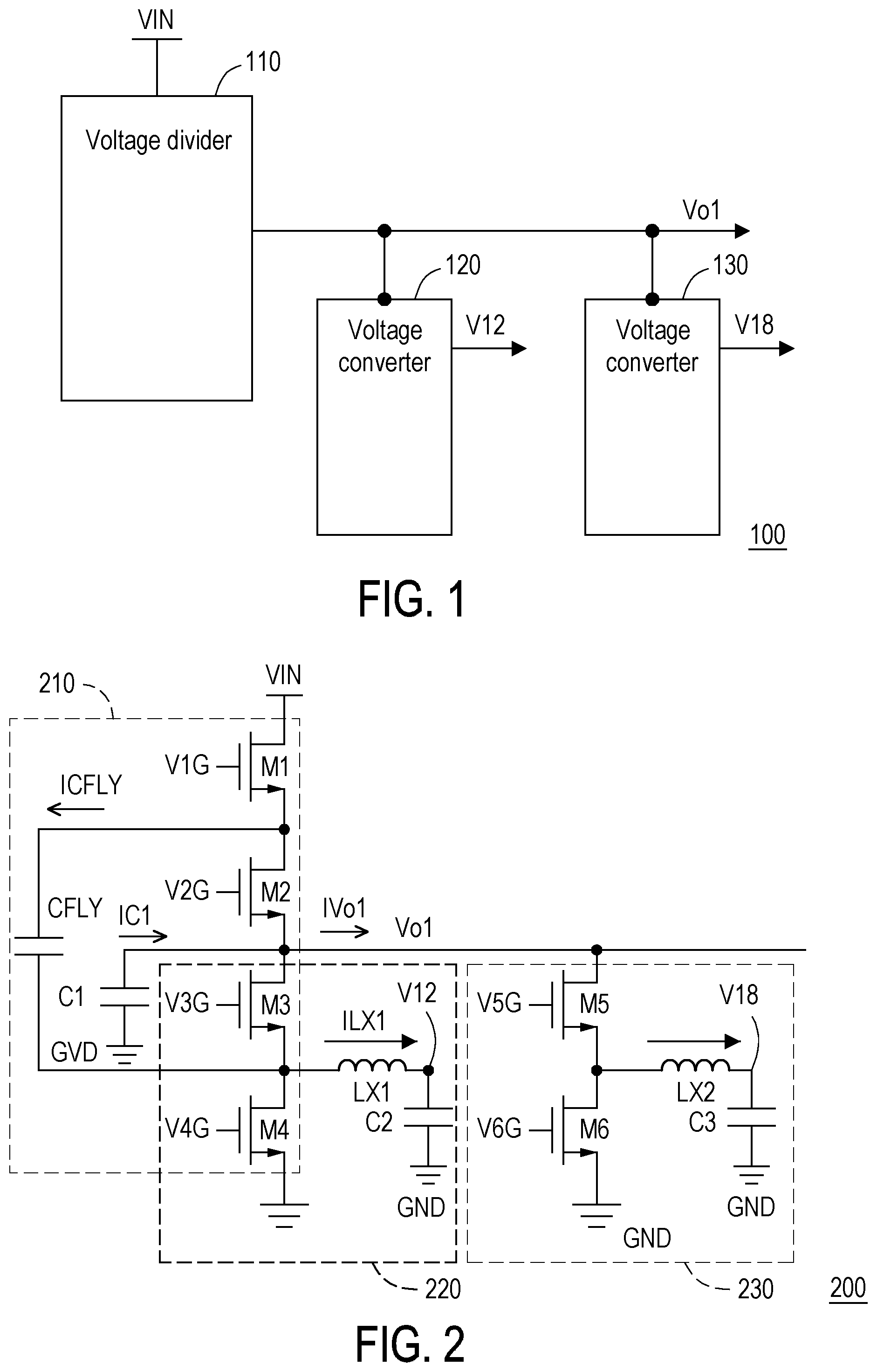
Please refer to , which illustrates a schematic diagram of a multiple output voltage generator according to an embodiment of present disclosure. The multiple output voltage generator 100 includes a voltage divider 110 , a first and second voltage converters 120 and 130 . The voltage divider 110 receives a power voltage VIN, and generates a first output voltage Vo 1 by dividing the power voltage VIN. The first and second voltage converters 120 and 130 are coupled to an output end of the voltage divider 110 in parallel. The first voltage converter 120 receives the first output voltage Vo 1 and generates a second output voltage V 12 according to the first output voltage Vo 1 . The second voltage converter 130 receives the first output voltage Vo 1 and generates a third output voltage V 18 according to the first output voltage Vo 1 . In present embodiment, both of the second output voltage V 12 and the third output voltage V 18 are smaller than the first output voltage Vo 1 .
It should be noted here, the voltage divider 110 generates the first output voltage Vo 1 by dividing the power voltage VIN. In some embodiment, the first output voltage Vo 1 may be half of the power voltage VIN. Such as that, the first output voltage Vo 1 is smaller than the power voltage VIN. Further, the voltage divider 110 provides the first output voltage Vo 1 to be operation powers of the first and second voltage converters 120 and 130 . That is, the first and second voltage converters 120 and 130 may be operated based on the first output voltage Vo 1 with a relative low voltage value, and power consumption of the first and second voltage converters 120 and 130 can be reduced. Moreover, by reducing power voltages of the first and second voltage converters 120 and 130 , the first and second voltage converters 120 and 130 may be implemented by circuit components with low voltage endurance. Such as that, circuit size and cost of the multiple output voltage generator 100 can be reduced.
On the other hand, in present disclosure, each of the first and second voltage converters 120 and 130 may be DC to DC converter or a low drop-out (LDO) voltage regulator. In some embodiment, both of the first and second voltage converters 120 and 130 may be DC to DC converters, and the two DC to DC converters may have different circuit structures.
Please refer to , which illustrates a schematic diagram of a multiple output voltage generator according to another embodiment of present disclosure. The multiple output voltage generator 200 includes a voltage divider 210 , a first and second voltage converters 220 and 230 . In this embodiment, the voltage divider 210 includes transistors M 1 to M 4 and capacitors C 1 and CFLY. The transistors M 1 to M 4 are coupled in series between a power voltage VIN and a reference ground end GND. The capacitor CFLY is coupled between a coupling end of the transistors M 1 and M 2 and a coupled end of the transistors M 3 and M 4 . The capacitor C 1 is coupled between a coupling end of the transistors M 2 and M 3 and the reference ground end GND. The coupling end of the transistors M 2 and M 3 performs an output end of the voltage divider 210 for outputting a first output voltage Vo 1 . Control ends of the transistors M 1 to M 4 respectively receive control signals V 1 G to V 4 G, and the transistors M 1 to M 4 may perform switching operation according to the control signals V 1 G to V 4 G.
Please refer to and commonly. . illustrates waveform plot of the first voltage converter of the according to multiple output voltage generator according to an embodiment of present disclosure. About detail operation of the voltage divider 210 , at a first phase (time period TP 1 ), the control signals V 1 G and V 3 G are at a high voltage level, and the control signals V 2 G and V 4 G is at a low voltage level, such that the transistors M 1 and M 3 may be turned on according to the control signals VG 1 and VG 3 simultaneously and the transistors M 2 and M 4 may be cut off according to the control signals VG 2 and VG 4 simultaneously. The control signal V 1 G is complementary to the control signal V 2 G. The control signals V 1 G and V 3 G have same waveforms and the control signals V 2 G and V 4 G have same waveforms. In this manner, the capacitors CFLY may be coupled to the capacitor C 1 in series between the power voltage VIN and the reference ground end. During the first phase, both of the capacitors CFLY and C 1 are charged by the power voltage VIN. A voltage VCFLY on the capacitor CFLY can be charged to the power voltage VIN through the turned-on transistor M 1 , and the first output voltage Vo 1 can be charged to half of the power voltage VIN(=VIN/2) by dividing the power voltage VIN if capacitances of the capacitors CFLY and C 1 are same.
Besides, the first output voltage Vo 1 may be fed to the inductor LX 1 through the turned-on transistor M 3 . Such as that, a voltage VLX 1 on the inductor LX 1 may be raised to VIN/2 during the first phase.
At a second phase (time period TP 2 ) after the first phase, the control signals V 1 G and V 3 G transit to the high voltage level, and the control signals V 2 G and V 4 G transit to the high voltage level, such that the transistors M 1 and M 3 may be cut off according to the control signals VG 1 and VG 3 simultaneously and the transistors M 2 and M 4 may be turned on according to the control signals VG 2 and VG 4 simultaneously. At this manner, the capacitors CFLY and CL may be coupled in parallel, the voltage VCFLY on the capacitor CFLY and the first output voltage Vo 1 are equaled by the parallel connected capacitors CFLY and C 1 , and charges in the capacitors CFLY and CL may be shared. Also, the voltage VLX 1 on the inductor LX 1 is pulled toward to a reference ground voltage by the turned-on transistor M 4 , and a second output voltage V 12 can be generated on a coupling end (a switching node) between the inductor LX 1 and the capacitor C 2 .
Time lengths of the first phase and the second phase may be same or different. In this embodiment, the time periods TP 1 and TP 2 may be different. That is, a duty cycle of each of the control signals V 1 G to V 4 G doesn't need to be 50%.
If conductive types of the transistors M 1 to M 4 are the same, phases of the control signals V 1 G and V 3 G are same, phases of the control signals V 2 G and V 4 G are same, and the phases of the control signals V 1 G and V 2 G are complementary.
In this embodiment, during the time period TP 1 , a current ILX 1 on the inductor LX 1 =a current ICFLY on the capacitor CFLY+a current IC 1 on the capacitor C 1 −a current Ivo 1 on the output end of the voltage divider 210 . During the time period TP 2 , the current ILX 1 on the inductor LX 1 =the current IC 1 on the capacitor C 1 +the current Ivo 1 on the output end of the voltage divider 210 . By the waveform of the voltage VLX 1 in , it can be seen that a voltage swing of the voltage VLX 1 is only VDD/2. That is, electromagnetic interference (EMI) caused by the first voltage converter 220 may be reduced efficiency, and a performance of the multiple output voltage generator 200 can be improved.
Please be noted here, since switching operation performed by the voltage divider 210 is a soft switching behavior. That is, no extra power loss may be occurred in the operation, and the voltage divider 210 provides higher voltage conversion efficiency than a voltage converter. Also, the first output voltage Vo 1 is generated by charge sharing by the capacitors C 1 and CFLY, and the first output voltage Vo 1 can be fixed to a target value (=½*VIN).
In this embodiment, only the transistor M 1 receives the power voltage with high voltage value. That is, voltage endurance of any one of the transistors M 2 to M 4 may be lower than a voltage endurance of the transistor M 1 . A circuit size of the voltage divider 210 may be reduced by implementing the transistors M 2 to M 4 by low voltage endurance components.
On the other hand, in this embodiment, the first and second voltage converters 220 and 230 are DC to DC voltage converters. The first voltage converter 220 is a buck converter, and includes the transistors M 3 and M 4 , an inductor LX 1 and a capacitor C 2 . The inductor LX 1 and the capacitor C 2 are coupled in series between a coupling end of the transistors M 3 and M 4 and the reference ground end GND. In this embodiment, the first voltage converter 220 and the voltage divider 210 share the transistors M 3 and M 4 .
The second voltage converter 230 includes transistors M 5 and M 6 , an inductor LX 2 and a capacitor C 3 . The transistors M 5 and M 6 are coupled in series between the output end of the voltage divider 210 and the reference ground end GND. Control ends of the transistors M 5 and M 6 respectively receive control signals V 5 G and V 6 G. The inductor LX 2 and the capacitor C 3 are coupled in series between a coupling end of the transistors M 5 and M 6 and the reference ground end GND.
Detail operation of the second voltage converter 230 is same to the first voltage converter 220 , and no more repeated description here.
The transistors M 5 and M 6 can be alternatively turned-on and cut-off, and a third output voltage V 18 can be generated at a coupling end (a switching node) of the inductor LX 2 and the capacitor C 3 . Since the transistors M 5 and M 6 receive the power voltage VIN as the operation power, the transistors M 5 and M 6 may be implemented by low voltage endurance components, and circuit size can be reduced.
Please be noted here, in this embodiment, the second output voltage V 12 may be smaller than the third output voltage V 18 .
Please refer to , which illustrates a schematic diagram of a multiple output voltage generator according to another embodiment of present disclosure. The multiple output voltage generator 400 includes a voltage divider 410 and a first and second voltage converters 420 and 430 . The voltage divider 410 includes transistors M 1 to M 4 and capacitors C 1 and CFLY. The transistors M 1 to M 4 are respectively controlled by control signals V 1 G to V 4 G. Detail operations of the voltage divider 410 is same as the voltage divider 210 in , and no more repeated description here.
The first voltage converter 420 includes the transistors M 3 and M 4 , an inductor LX 1 and a capacitor C 2 . Also, detail operation of the first voltage converter 420 is same as the first voltage converter 220 in , and no more repeated description here.
The second voltage converter 430 is a low-dropout voltage regulator, and includes a feedback resistor 431 , an error amplifier 432 and a transistor M 7 . The feedback resistor 431 may receive a third output voltage V 18 of the second voltage converter 430 , and generate the feedback voltage VFB 1 according to the third output voltage V 18 . The error amplifier 432 has a negative input end for receiving the feedback voltage, and a positive input end for receiving a reference voltage VREF 1 . A first end of the transistor M 7 receives the first output voltage Vo 1 , and a second end of the transistor M 7 generates the third output voltage V 18 . A control end of the transistor M 7 is coupled to an output end of the error amplifier 432 .
In detail, the feedback resistor 431 may be a resistor string and be used to divide the second output voltage V 18 to generate the feedback voltage VFB 1 . The error amplifier 432 compares the feedback voltage VFB 1 with the reference voltage VREF 1 , and amplifies an error between the feedback voltage VFB 1 and the reference voltage VREF 1 to control the transistor M 7 .
In this embodiment, by receiving the first output voltage Vo 1 as an operation power, a power efficiency of the second voltage converter 430 which is a low-dropout voltage regulator can be improved.
In this embodiment, the reference voltage VREF 1 may be a preset voltage.
Please refer to , which illustrates a schematic diagram of a multiple output voltage generator according to another embodiment of present disclosure. The multiple output voltage generator 500 includes a voltage divider 510 and a first and second voltage converters 520 and 530 . Different from the multiple output voltage generator 400 , in this embodiment, the first voltage converter 520 is a low-drop out voltage generator, and the second voltage converter 530 is a DC to DC converter. The first voltage converter 520 includes a feedback resistor 521 , an error amplifier 522 and a transistor M 7 . The feedback resistor 521 receives a second output voltage V 12 and generates a feedback voltage VFB 2 by dividing the second output voltage V 12 . The error amplifier 522 amplifies an error between the feedback voltage VFB 2 and a reference voltage VREF 2 to control the transistor M 7 . The transistor M 7 receives the first out voltage Vo 1 and generates the second output voltage V 12 .
The second voltage converter 530 includes transistors M 5 and M 6 , an inductor LX 2 and a capacitor C 2 . The second voltage converter 530 may be a buck converter. The transistors M 5 and M 6 are coupled in series between the first output voltage Vo 1 and the reference ground end GND, and are respectively controlled by control signals V 5 G and V 6 G. The inductor LX 2 and the capacitor C 2 are coupled in series between a coupling end of the transistors M 5 and M 6 and the reference ground end. The second voltage converter 530 receives the first output voltage Vo 1 as an operation power, and generates a third output voltage V 18 by converting the first output voltage Vo 1 .
In this embodiment, the reference voltage VREF 2 may be a preset voltage.
Please refer to and commonly, wherein illustrates a schematic diagram of a control signal generator for the voltage divider of the multiple output voltage generator according to an embodiment of present disclosure. The control signal generator 600 is used to generate the control signals V 1 G to V 4 G for controlling operations of the voltage divider 210 . The control signal generator 600 includes a feedback resistor 610 , an error amplifier 620 , a ramp signal generator 630 , a comparator 640 and a logic and driving circuit 650 . The feedback resistor 610 may receive the second output voltage V 12 and generate a feedback voltage VFB 3 by dividing the second output voltage V 12 . The feedback resistor 610 provides the feedback voltage VFB 3 to a negative input end of the error amplifier 620 . The error amplifier 620 also receives a reference voltage VREF 3 by a positive input end. The error amplifier 620 generates a signal CS 1 according to a difference of the feedback voltage VFB 3 and the reference voltage VREF 3 .
The ramp signal generator 630 generates a reference ramp signal RS 1 to a positive input end of the comparator 640 . The error amplifier 620 provides the signal CS 1 to a negative input end of the comparator 640 . The comparator 640 generates a signal CP 1 by comparing the reference ramp signal RS 1 with the signal CS 1 .
The logic and driving circuit 650 receives the signal CP 1 and generates, based on a clock signal CLK 1 , the control signals V 1 G to V 4 G according to the signal CP 1 . The logic and driving circuit 650 may include a logic circuit core for performing logic operation on the signal CP 1 to generate operation results. The logic and driving circuit 650 may also include a driving part to amplify to operation results to generate the control signals V 1 G to V 4 G.
In this embodiment, the reference voltage VREF 3 may be a preset voltage.
Please refer to and commonly, wherein illustrates a schematic diagram of a control signal generator for the voltage converter of the multiple output voltage generator according to an embodiment of present disclosure. The control signal generator 700 is used to generate the control signals V 5 G and V 6 G for controlling the second voltage converter 230 . The control signal generator 700 includes a feedback resistor 710 , an error amplifier 720 , a ramp signal generator 730 , a comparator 740 and a logic and driving circuit 750 . The feedback resistor 710 may receive the third output voltage V 18 and generate a feedback voltage VFB 34 by dividing the third output voltage V 18 . The feedback resistor 710 provides the feedback voltage VFB 4 to a negative input end of the error amplifier 720 . The error amplifier 720 also receives a reference voltage VREF 4 by a positive input end. The error amplifier 720 generates a signal CS 2 according to a difference of the feedback voltage VFB 4 and the reference voltage VREF 4 .
The ramp signal generator 730 generates a reference ramp signal RS 2 to a positive input end of the comparator 740 . The error amplifier 720 provides the signal CS 2 to a negative input end of the comparator 740 . The comparator 740 generates a signal CP 2 by comparing the reference ramp signal RS 2 with the signal CS 2 .
The logic and driving circuit 750 receives the signal CP 2 and generates, based on a clock signal CLK 2 , the control signals V 5 G and V 6 G according to the signal CP 2 . The logic and driving circuit 750 may include a logic circuit core for performing logic operation on the signal CP 2 to generate operation results. The logic and driving circuit 750 may also include a driving part to amplify to operation results to generate the control signals V 5 G and V 6 G.
In this embodiment, the reference voltage VREF 4 may be a preset voltage.
Please refer to , which illustrates a schematic diagram of a multiple output voltage generator according to another embodiment of present disclosure. The multiple output voltage generator 800 includes a voltage divider 810 , a first voltage converter 820 , a second voltage converter 830 and a third voltage converter 840 . The voltage divider 810 receive a power voltage VIN, and generates a first output voltage Vo 1 by dividing the power voltage VIN. In some embodiment, the first output voltage Vo 1 may be half of the power voltage VIN.
The first voltage converter 820 , the second voltage converter 830 and the third voltage converter 840 are coupled to an output end of the voltage divider 110 in parallel. All of the first voltage converter 820 , the second voltage converter 830 and the third voltage converter 840 receive the first output voltage Vo 1 as operation powers, and the first voltage converter 820 , the second voltage converter 830 and the third voltage converter 840 respectively generate a second output voltage V 12 , a third output voltage V 18 and a fourth output voltage V 33 .
In some embodiment, the first output voltage Vo 1 is larger than each of the second output voltage V 12 , the third output voltage V 18 and the fourth output voltage V 33 . On the other hand, the second output voltage V 12 may be smaller than the third output voltage V 18 , and the third output voltage V 18 may be smaller than the fourth output voltage V 33 .
In this embodiment, each of the first, second and third voltage converters 820 , 830 and 840 may be DC to DC converter or a low drop-out (LDO) voltage regulator.
Please refer to , which illustrates a schematic diagram of a multiple output voltage generator according to another embodiment of present disclosure. The multiple output voltage generator 900 includes a voltage divider 910 and a first to third voltage converters 920 to 940 . Th voltage divider 910 includes transistors M 1 to M 4 and capacitors CFLY and C 1 . Detail operation of the voltage divider 410 is same as the voltage divider 210 in , and no more repeated description here.
In this embodiment, both of the first to second voltage converters 920 to 930 are DC to DC converters. The third voltage converter 940 is a low drop-out voltage regulator. The first voltage converter 920 includes the transistors M 3 and M 4 , an inductor LX 1 and a capacitor C 2 . The second voltage converter 930 includes transistors M 5 and M 6 , an inductor LX 2 and a capacitor C 3 . Detail operation of the first voltage converter 920 and the second voltage converter 930 is same to the first voltage converter 220 , and no more repeated description here.
The third voltage converter 940 may include a transistor M 7 , and detail operation of the third voltage converter 940 is same to the second voltage converter 430 , and no more repeated description here.
It should be noted here, the multiple output voltage generator 900 may provide the first output voltage Vo 1 to drive a load circuit 901 . The load circuit 901 may be an internal circuit for a system, or the load circuit 901 may be a pre-driver for the DC to DC voltage converters used in the multiple output voltage generator 900 . By reducing an operation voltage of the pre-driver, a quiescent current of the DC to DC voltage converters can be reduced, too.
In summary, if a power voltage is much higher than a second output voltage. To generate the second output voltage by converting the power voltage directly may generate large amount of power conversion loss. In this disclosure, the multiple output voltage generator may divide the power voltage and then convert the first output voltage to generate another output voltage. That is, power conversion loss can be reduced, and a conversion efficiency of the multiple output voltage generator can be improved.
It will be apparent to those skilled in the art that various modifications and variations can be made to the structure of the disclosed embodiments without departing from the scope or spirit of the disclosure. In view of the foregoing, it is intended that the disclosure cover modifications and variations of this disclosure provided they fall within the scope of the following claims and their equivalents.
Figures (7)
Citations
This patent cites (25)
- US7132765
- US10135336
- US10637356
- US11362585
- US20090039947
- US20120154013
- US20140268946
- US20150130367
- US20150188362
- US20160118886
- US20160329810
- US20170324321
- US20170331374
- US20190190373
- US20190348913
- US20200161959
- US20210067033
- US20210184571
- US20220029534
- US20220075401
- US20220231601
- US20220231618
- US20230006555
- US20230029565
- US20230050531