Switched-capacitor Power Stage and Switched-capacitor Converter
Abstract
A switched-capacitor power stage includes a first sub-power stage. The first sub-power stage includes a first inductor, a first high switch, a first low switch, and a first set of switched-capacitor networks. The first inductor is coupled to an input terminal. The first high switch is coupled between the first inductor and an output terminal. The first low switch is coupled between the first inductor and a first transition node. The first set of switched-capacitor networks is coupled between the first transition node and the output terminal.
Claims (15)
1. A switched-capacitor power stage, comprising: a first sub-power stage comprising: a first inductor coupled to an input terminal; a first high switch coupled between the first inductor and an output terminal; a first low switch coupled between the first inductor and a first transition node; and a first set of switched-capacitor networks coupled between the first transition node and the output terminal, wherein when the first high switch is turned off and the first low switch is turned on, the first inductor and the first set of switched-capacitor networks are coupled in series; and a second sub-power stage comprising: a second inductor coupled to the input terminal; a second high switch coupled between the second inductor and the output terminal; a second low switch coupled between the second inductor and a second transition node; and a second set of switched-capacitor networks coupled between the second transition node and the output terminal.
7. A switched-capacitor converter, comprising: a plurality of sub-power stages, wherein each of the sub-power stages comprises: an inductor coupled to an input terminal; a high switch coupled between the inductor and an output terminal; a low switch coupled between the inductor and a transition node; a set of switched-capacitor networks coupled between the transition node and the output terminal; and a driver configured to control the set of switched-capacitor networks; and a controller configured to generate a plurality of control signals and a plurality of enable signals according to an output voltage at the output terminal, a first reference voltage, and a second reference voltage, wherein the driver is further configured to generate a plurality of gate signals according to the control signals and the enable signals to control a plurality of switches in the set of switched-capacitor networks.
Show 13 dependent claims
2. The switched-capacitor power stage of claim 1 , wherein a transition voltage at the first transition node is greater than an input voltage at the input terminal.
3. The switched-capacitor power stage of claim 1 , further comprising: a third sub-power stage comprising: a third inductor coupled to the input terminal; a third high switch coupled between the third inductor and the output terminal; a third low switch coupled between the third inductor and a third transition node; and a third set of switched-capacitor networks coupled between the third transition node and the output terminal.
4. The switched-capacitor power stage of claim 1 , wherein the first set of switched-capacitor networks comprises a first switched-capacitor network and a second switched-capacitor network, wherein each of the first switched-capacitor network and the second switched-capacitor network comprises: a first switch coupled between the first transition node and a first inner node; a second switch coupled between the first inner node and the output terminal; a third switch configured to receive a voltage and coupled to a second inner node; a fourth switch coupled between the second inner node and the output terminal; and a capacitor coupled between the first inner node and the second inner node.
5. The switched-capacitor power stage of claim 4 , wherein a working period comprises a first time interval, a second time interval, a third time interval, and a fourth time interval sequentially, wherein in the first time interval and in the third time interval, the first high switch is turned on and the first low switch is turned off, wherein in the second time interval and in the fourth time interval, the first high switch is turned off and the first low switch is turned on.
6. The switched-capacitor power stage of claim 5 , wherein in the first time interval and in the second time interval, the first switch of the first switched-capacitor network, the fourth switch of the first switched-capacitor network, the second switch of the second switched-capacitor network, and the third switch of the second switched-capacitor network are turned on, and the second switch of the first switched-capacitor network, the third switch of the first switched-capacitor network, the first switch of the second switched-capacitor network, and the fourth switch of the second switched-capacitor network are turned off, wherein in the third time interval and in the fourth time interval, the first switch of the first switched-capacitor network, the fourth switch of the first switched-capacitor network, the second switch of the second switched-capacitor network, and the third switch of the second switched-capacitor network are turned off, and the second switch of the first switched-capacitor network, the third switch of the first switched-capacitor network, the first switch of the second switched-capacitor network, and the fourth switch of the second switched-capacitor network are turned on.
8. The switched-capacitor converter of claim 7 , wherein the driver is further configured to output the control signals to control the high switches and the low switches in the sub-power stages.
9. The switched-capacitor converter of claim 7 , wherein the controller comprises: a pulse control loop circuit configured to generate the control signals according to a transition voltage at the transition node and the first reference voltage; and a frequency control loop circuit configured to generate the enable signals according to the output voltage and the second reference voltage.
10. The switched-capacitor converter of claim 9 , wherein the pulse control loop circuit comprises: a sample and hold circuit configured to generate first signals according to the transition voltage; a mismatch calibration circuit configured to generate second signals according to the first signals and the first reference voltage; and a timing logic circuit configured to generate the control signals according to the second signals.
11. The switched-capacitor converter of claim 9 , wherein the frequency control loop circuit comprises: an operation amplifier configured to generate a comparison signal according to the output voltage and the second reference voltage; a voltage-controlled oscillator configured to generate a frequency clock signal according to the comparison signal; a counter configured to generate a plurality of counting signals according to the frequency clock signal; and a finite state machine circuit configured to generate the enable signals according to the counting signals.
12. The switched-capacitor converter of claim 11 , wherein the frequency control loop circuit further comprises: a phase divider configured to generate phase signals according to the frequency clock signal and output the phase signals to the pulse control loop circuit.
13. The switched-capacitor converter of claim 11 , wherein the frequency control loop circuit further comprises: a buffer coupled between the operation amplifier and the voltage-controlled oscillator.
14. The switched-capacitor converter of claim 7 , wherein each of the set of switched-capacitor networks comprises a first converter cell, a second converter cell, a third converter cell, and a fourth converter cell, wherein each of the first converter cell, the second converter cell, the third converter cell, and the fourth converter cell comprises: a first switch coupled between the transition node and a first inner node; a second switch coupled between the first inner node and the output terminal; a third switch coupled to a second inner node; a fourth switch coupled between the second inner node and the output terminal; and a capacitor coupled between the first inner node and the second inner node.
15. The switched-capacitor converter of claim 14 , wherein a capacitance value of the capacitor in the second converter cell is twice a capacitance value of the capacitor in the first converter cell, a capacitance value of the capacitor in the third converter cell is twice the capacitance value of the capacitor in the second converter cell, and a capacitance value of the capacitor in the fourth converter cell is twice the capacitance value of the capacitor in the third converter cell.
Full Description
Show full text →
BACKGROUND
Technical Field
The present disclosure relates to converter technology. More particularly, the present disclosure relates to a switched-capacitor power stage and a switched-capacitor converter.
Description of Related Art
With development of technology, switched-capacitor (SC) converters have been applied to various circuits. In some related arts, a voltage conversion ratio (VCR) of a switched-capacitor converter is better but switching loss, ripple, and hard charging loss are larger. In some related arts, switching loss, ripple, and hard charging loss of a switched-capacitor converter are smaller but a voltage conversion ratio of the switched-capacitor converter is limited (e.g., too small).
SUMMARY
Some aspects of the present disclosure are to provide a switched-capacitor power stage. The switched-capacitor power stage includes a first sub-power stage. The first sub-power stage includes a first inductor, a first high switch, a first low switch, and a first set of switched-capacitor networks. The first inductor is coupled to an input terminal. The first high switch is coupled between the first inductor and an output terminal. The first low switch is coupled between the first inductor and a first transition node. The first set of switched-capacitor networks is coupled between the first transition node and the output terminal.
Some aspects of the present disclosure are to provide a switched-capacitor converter. The switched-capacitor converter includes a plurality of sub-power stages and a controller. Each of the sub-power stages includes an inductor, a high switch, a low switch, a set of switched-capacitor networks, and a driver. The inductor is coupled to an input terminal. The high switch is coupled between the inductor and an output terminal. The low switch is coupled between the inductor and a transition node. The set of switched-capacitor networks are coupled between the transition node and the output terminal. The driver is configured to control the set of switched-capacitor networks. The controller is configured to generate a plurality of control signals and a plurality of enable signals according to an output voltage at the output terminal, a first reference voltage, and a second reference voltage. The driver is further configured to generate a plurality of gate signals according to the control signals and the enable signals to control a plurality of switches in the set of switched-capacitor networks.
BRIEF DESCRIPTION OF THE DRAWINGS
The disclosure can be more fully understood by reading the following detailed description of the embodiment, with reference made to the accompanying drawings as follows:
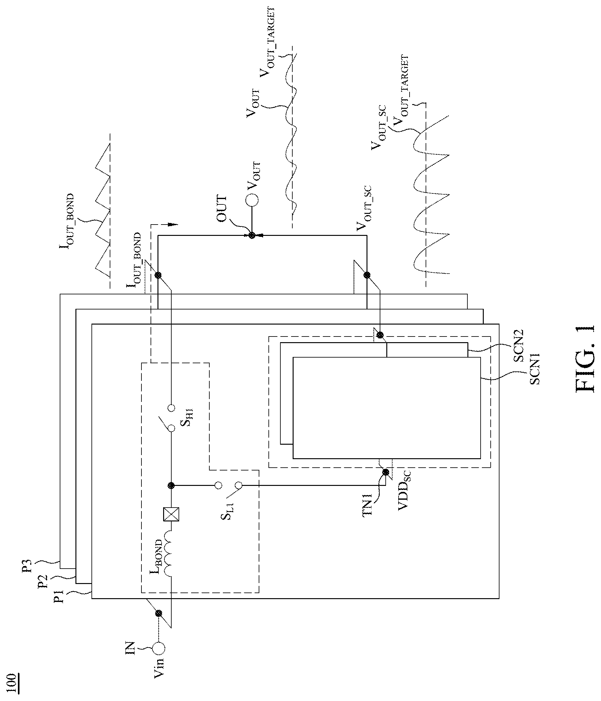
is a schematic diagram illustrating a switched-capacitor power stage according to some embodiments of the present disclosure.
A is a schematic diagram illustrating the switched-capacitor power stage in operating in a first phase according to some embodiments of the present disclosure.
B is a schematic diagram illustrating waveforms of signals associated with A according to some embodiments of the present disclosure.
A is a schematic diagram illustrating the switched-capacitor power stage in operating in a second phase according to some embodiments of the present disclosure.
B is a schematic diagram illustrating waveforms of signals associated with A according to some embodiments of the present disclosure.
is a schematic diagram illustrating a switched-capacitor power stage according to some embodiments of the present disclosure.
is a schematic diagram illustrating operations of the switched-capacitor networks in in four time intervals according to some embodiments of the present disclosure.
is a schematic diagram illustrating a split structure of the switched-capacitor networks in according to some embodiments of the present disclosure.
is a schematic diagram illustrating a switched-capacitor converter according to some embodiments of the present disclosure.
is a schematic diagram illustrating a pulse control loop circuit in according to some embodiments of the present disclosure.
is a schematic diagram illustrating waveforms of signals in sub-power stages according to some embodiments of the present disclosure.
is a schematic diagram illustrating a buffer coupled between an operation amplifier and a voltage-controlled oscillator according to some embodiments of the present disclosure.
DETAILED DESCRIPTION
In the present disclosure, “connected” or “coupled” may refer to “electrically connected” or “electrically coupled.” “Connected” or “coupled” may also refer to operations or actions between two or more elements.
Reference is made to . is a schematic diagram illustrating a switched-capacitor power stage 100 according to some embodiments of the present disclosure.
As illustrated in , the switched-capacitor power stage 100 includes a plurality of sub-power stages P 1 -P 3 . These sub-power stages P 1 -P 3 have similar structures. For the purpose of simplicity and ease of understanding, following paragraphs takes the sub-power stage P 1 as an example.
The sub-power stage P 1 includes an inductor L BOND , a high switch S H1 , a low switch S L1 , and a set of switched-capacitor networks SCN 1 -SCN 2 . The inductor L BOND is coupled to an input terminal IN. An input voltage V IN is received at the input terminal IN. The high switch S H1 is coupled between the inductor L BOND and an output terminal OUT. The low switch S L1 is coupled between the inductor L BOND and a transition node TN 1 . The set of switched-capacitor networks SCN 1 -SCN 2 is coupled between the transition node TN 1 and the output terminal OUT. The inductor L BOND can be implemented by a bonding wire.
By controlling the high switch S H1 and the low switch S L1 , a current I OUT_BOND is generated and flows through the inductor L BOND and a transition voltage VDD SC is generated at the transition node TN 1 . The set of switched-capacitor networks SCN 1 -SCN 2 generates a voltage V OUT_SC according to the transition voltage VDD SC . Then, an output voltage V OUT is generated at the output terminal OUT according to the voltage V OUT_SC and a voltage corresponding to the current I OUT_BOND . As waveforms illustrated in , compared to the voltage V OUT_SC , the output voltage V OUT is closer to a target voltage V OUT_TARGET .
The quantity of the sub-power stages of the switched-capacitor power stage 100 is merely illustration, and the present disclosure is not limited thereto.
The switched-capacitor power stage 100 can operate in two phases.
A is a schematic diagram illustrating the switched-capacitor power stage 100 in operating in a first phase according to some embodiments of the present disclosure. B is a schematic diagram illustrating waveforms of signals associated with A according to some embodiments of the present disclosure. A is a schematic diagram illustrating the switched-capacitor power stage 100 in operating in a second phase according to some embodiments of the present disclosure. B is a schematic diagram illustrating waveforms of signals associated with A according to some embodiments of the present disclosure.
As illustrated in A and B , in the first phase (e.g., ØA), the high switch S H1 is turned on by a switching signal CLK SH and the low switch S L1 is turned off by a switching signal CLK SL . In other words, the switching signal CLK SH has an enable level in the first phase, and the switching signal CLK SL has a disable level in the first phase. Under this condition, the input voltage V IN can charge (e.g., the current I OUT_BOND ) the output terminal OUT through the inductor L BOND and the high switch S H1 to increase the output voltage VOUT. The inductor L BOND can also store power from the input voltage V IN . In addition, switches in the set of switched-capacitor networks SCN 1 -SCN 2 can be controlled such that a fly capacitor in the set of switched-capacitor networks SCN 1 -SCN 2 can charge the output terminal OUT to increase the output voltage VOUT. This fly capacitor is controlled by a switching signal CLK SC .
As illustrated in A and B , since the inductor L BOND can provide an additional current to the output terminal OUT in the first phase, the output voltage V OUT can drop smoothly. Hence, the ripple can be reduced.
As illustrated in A and B , in the second phase (e.g., ØB), the high switch S H1 is turned off by the switching signal CLK SH and the low switch S L1 is turned on by a switching signal CLK SL . In other words, the switching signal CLK SH has a disable level in the second phase, and the switching signal CLK SL has an enable level in the second phase. Under this condition, power stored in the inductor L BOND can be used to charge the transition node TN 1 to increase the transition voltage VDD SC , and the transition voltage VDD SC can charge the output terminal OUT to support the output voltage V OUT . By controlling duties of the switching signal CLK SH and the switching signal CLK SL , an appropriate transition voltage VDD SC can be generated.
As illustrated in A and B , since the inductor L BOND can act as a voltage source to make the transition voltage VDD SC at the transition node TN 1 be greater than the input voltage V IN at the input terminal IN, a voltage conversion ratio (VCR) of one converter cell in the switched-capacitor power stage 100 can be larger.
References is made to . is a schematic diagram illustrating a switched-capacitor power stage 400 according to some embodiments of the present disclosure. The switched-capacitor power stage 400 is similar to the switched-capacitor power stage 100 in . As illustrated in and taking the switched-capacitor network SCN 1 as an example, the switched-capacitor network SCN 1 includes a switch S 1,1 , a switch S 1,2 , a switch S 1,3 , a switch S 1,4 , and a fly capacitor C 1 . The switch S 1,1 is coupled between the transition node TN 1 and an inner node NN 1 . The switch S 1,2 is coupled between the inner node NN 1 and the output terminal OUT. The switch S 1,3 is configured to receive a voltage V SS and coupled to an inner node NN 2 . The switch S 1,4 is coupled between the inner node NN 2 and the output terminal OUT. The fly capacitor C 1 is coupled between the inner node NN 1 and the inner node NN 2 . In the embodiment of , the switch S 1,1 , the switch S 1,2 , and the switch S 1,4 are implemented by P-type transistors, and the switch S 1,3 is implemented by a N-type transistor, but the present disclosure is not limited thereto.
The switched-capacitor network SCN 2 has a similar structure, so it is not described herein again. References is made to . is a schematic diagram illustrating operations of the switched-capacitor networks SCN 1 -SCN 2 in in four time intervals according to some embodiments of the present disclosure. Similar to the switched-capacitor network SCN 1 in , the switched-capacitor network SCN 2 includes a switch S 2,1 , a switch S 2,2 , a switch S 2,3 , a switch S 2,4 , and a fly capacitor C 2 .
Taking the sub-power stage P 1 as an example, a working period includes a time interval TD 1 , a time interval TD 2 , a time interval TD 3 , and a time interval TD 4 sequentially. The time interval TD 1 and the time interval TD 3 correspond to the aforementioned first phase (e.g., ØA), and the time interval TD 2 and the time interval TD 4 correspond to the aforementioned second phase (e.g., ØB). In other words, in the time interval TD 1 (e.g., Ø 1 A) and the time interval TD 3 (e.g., Ø 2 A), the high switch S H1 of the sub-power stage P 1 is turned on and the low switch S L1 of the sub-power stage P 1 is turned off. In the time interval TD 2 (e.g., Ø 1 B) and the time interval TD 4 (e.g., Ø 2 B), the high switch S H1 of the sub-power stage P 1 is turned off and the low switch S L1 of the sub-power stage P 1 is turned on.
As illustrated in , in the time interval TD 1 (e.g., Ø 1 A) and the time interval TD 2 (e.g., Ø 1 B), the switch S 1,1 and the switch S 1,4 of the switched-capacitor networks SCN 1 and the switch S 2,3 and the switch S 2,2 of the switched-capacitor networks SCN 2 are turned on. In addition, the switch S 1,2 and the switch S 1,3 of the switched-capacitor networks SCN 1 and the switch S 2,1 and the switch S 2,4 of the switched-capacitor networks SCN 2 are turned off.
On the contrary, in the time interval TD 3 (e.g., Ø 2 A) and the time interval TD 4 (e.g., Ø 2 B), the switch S 1,2 and the switch S 1,3 of the switched-capacitor networks SCN 1 and the switch S 2,1 and the switch S 2,4 of the switched-capacitor networks SCN 2 are turned on. In addition, the switch S 1,1 and the switch S 1,4 of the switched-capacitor networks SCN 1 and the switch S 2,3 and the switch S 2,2 of the switched-capacitor networks SCN 2 are turned off.
As illustrated in and B , in the time interval TD 1 (e.g., Ø 1 A) and the time interval TD 3 (e.g., Ø 2 A), the inductor L BOND is coupled with the switched-capacitor networks SCN 1 -SCN 2 in a parallel form when the output voltage OUT decreases. The inductor L BOND can act as a current source to provide an additional current I OUT_BOND to support the output voltage V OUT . Hence, the output voltage V OUT drops smoothly and the ripple can be reduced.
As illustrated in and B , in the time interval TD 2 (e.g., Ø 1 B) and the time interval TD 4 (e.g., Ø 2 B), the inductor L BOND is coupled with the switched-capacitor networks SCN 1 -SCN 2 in a series form. The inductor L BOND can act as a voltage source to make the transition voltage VDD SC higher than the input voltage V IN . Hence, the output voltage V OUT can be higher than V IN /2. In other words, the voltage conversion ration can be greater than ½.
The aforementioned operations in the time intervals TD 1 -TD 4 can reduce the ripple. The sub-power stages P 2 -P 3 have similar structures and operations, so they are not described herein again.
Compared to some related arts with more switches, the present disclosure has fewer switches, so the switching loss and the conduction loss in the present disclosure are smaller.
Compared to some related arts with the same number switches, in the present disclosure, more power is provide to the output voltage V OUT during each working period (e.g., the fly caps in the switched-capacitor networks SCN 1 -SCN 2 provide power in the first phase ØA and the inductor L BOND provides power in the second phase ØB), so the ripple and the hard charging loss in the present disclosure are smaller, and the switching frequency (switching loss) in the present disclosure can be smaller.
In addition, the present disclosure is suitable for applications with small capacitor sizes. Small capacitors are easily fully charged and the peak of the inductor current is low, so the conduction loss in the present disclosure is not increased too much. Further, the inductor L BOND acts as a current source to make the output voltage V OUT drop smoothly when the inductor L BOND is coupled with the switched-capacitor networks SCN 1 -SCN 2 in the parallel form (e.g., Ø 1 A and Ø 2 A), and the inductor L BOND acts as a voltage source to make the transition voltage VDD SC be greater than the input voltage V IN when the inductor L BOND is coupled with the switched-capacitor networks SCN 1 -SCN 2 (e.g., Ø 1 B and Ø 2 B) in the series form. Thus, the ripple can be smaller and the voltage conversion ration can be greater than ½ such that the efficiency is better.
References is made to . is a schematic diagram illustrating a split structure 600 according to some embodiments of the present disclosure. The split structure 600 illustrates that the switched-capacitor networks SCN 1 -SCN 2 in is split into converter cells. In some embodiments, each of the switched-capacitor networks SCN 1 and SCN 2 in can be split into a plurality of converter cells.
takes the switched-capacitor networks SCN 1 as an example. As illustrated in , the switched-capacitor network SCN 1 is split into multiple converter cells CELL 0 , CELL 1 , CELL 2 , and CELL 3 . Each of the converter cells CELL 0 , CELL 1 , CELL 2 , and CELL 3 has a structure similar to the switched-capacitor network SCN 1 in . Taking the converter cell CELL 0 as an example, the converter cell CELL 0 includes a switch S 1,1 [ 0 ], a switch S 1,2 [ 0 ], a switch S 1,3 [ 0 ], a switch S 1,4 [ 0 ], and a fly capacitor C 1 [ 0 ].
It is assumed that a capacitance value of the fly capacitor C 1 in is C FLY . Then, a capacitance value of the fly capacitor C 1 [ 0 ] in the converter cell CELL 0 can be C FLY /15, a capacitance value of the fly capacitor C 1 [ 1 ] in the converter cell CELL 1 can be 2C FLY /15, a capacitance value of the fly capacitor C 1 [ 2 ] in the converter cell CELL 2 can 4C FLY /15, and a capacitance value of the fly capacitor C 1 [ 3 ] in the converter cell CELL 3 can be 8C FLY /15. In other words, the capacitance value of the fly capacitor C 1 [ 1 ] is twice the capacitance value of the fly capacitor C 1 [ 0 ], the capacitance value of the fly capacitor C 1 [ 2 ] is twice the capacitance value of the fly capacitor C 1 [ 1 ], and the capacitance value of the fly capacitor C 1 [ 3 ] is twice the capacitance value of the fly capacitor C 1 [ 2 ].
By splitting each of the switched-capacitor networks SCN 1 and SCN 2 in into , the switch S 1,1 , the switch S 1,2 , the switch S 1,3 , the switch S 1,4 , and the capacitor C 1 in are split. Enable signals EN[ 0 ]-EN[ 3 ] (associated with operating frequency) are used to generate gate signals which are configured to control these switches so as to control the usage of these split capacitors. Hence, in a light load mode, power provide to the output terminal OUT is less by controlling the usage of the split capacitors. Since power provide to the output terminal OUT is less, less extra charges are accumulated on an output capacitor (e.g., an output capacitor C OUT in ). Thus, the ripple can be reduced and this can prevent the switching loss from increasing. The details about the enable signals EN[ 0 ]-EN[ 3 ] (the enable signals EN[ 0 : 3 ]) are described in following paragraphs.
The switched-capacitor network SCN 2 has a similar structure, so it is not described herein again.
Reference is made to . is a schematic diagram illustrating a switched-capacitor converter 700 according to some embodiments of the present disclosure. The switched-capacitor converter 700 includes a switched-capacitor power stage 710 and a controller 720 . The controller 720 is coupled to the switched-capacitor power stage 710 .
The switched-capacitor power stage 710 is similar to the switched-capacitor power stage 400 in with the split structure 600 in . Taking the sub-power stage P 1 as an example, the sub-power stage P 1 further includes a driver DR 1 , and the driver DR 1 is configured to control the high switches S H1 , the low switch S L1 , and the switches in the switched-capacitor networks SCN 1 -SCN 2 to be turned on or turned off.
The controller 720 is configured to generate control signals CS H1 , CS L1 , CS H2 , CS L2 , CS H3 , CS L3 and the enable signals EN[ 3 : 0 ] according to the output voltage VOUT at the output terminal OUT, a reference voltage V REF1 , and a reference voltage V REF2 .
As illustrated in , the controller 720 includes a pulse control loop circuit 721 , a frequency control loop circuit 722 , and the output capacitor C OUT .
The pulse control loop circuit 721 receives the transition voltage VDD SC from the switched-capacitor power stage 710 . The pulse control loop circuit 721 can generate the control signals control signals CS H1 , CS L1 , CS H2 , CS L2 , CS H3 , CS L3 according to the transition voltage VDD SC and the reference voltage V REF1 . is a schematic diagram illustrating the pulse control loop circuit 721 in according to some embodiments of the present disclosure. As illustrated in and , the pulse control loop circuit 721 includes a sample and hold circuit 7211 , a mismatch calibration circuit 7212 , and a timing logic circuit 7213 . The sample and hold circuit 7211 generates first signals FS 1 according to the transition voltage VDD SC . The mismatch calibration circuit 7212 generates second signals FS 2 according to the first signals FS 1 and the reference voltage V REF1 . The timing logic circuit 7213 generates the control signals CS H1 , CS L1 , CS H2 , CS L2 , CS H3 , CS L3 according to the second signals FS 2 and phase Signals V PHASE1 -V PHASE3 .
The driver DR 1 in the sub-power stage P 1 can receive the control signals CS H1 , CS L1 , and output the control signals CS H1 , CS L1 to control the high switches S H1 and the low switch S L1 in the sub-power stage P 1 respectively. By adjusting duties of the control signals CS H1 , CS L1 to turn on or turn off the high switches S H1 and the low switch S L1 , the transition voltage VDD SC can have an appropriate value with respective to the output voltage V OUT .
The frequency control loop circuit 722 and the output capacitor C OUT are coupled to the output terminal OUT. The frequency control loop circuit 722 can generate the enable signals EN[ 3 : 0 ] according to the output voltage V OUT and the reference voltage V REF2 .
As illustrated in , the frequency control loop circuit 722 includes an operation amplifier 7221 , a voltage-controlled oscillator 7222 , a phase divider 7223 , a counter 7224 , and a finite state machine circuit 7225 .
The operation amplifier 7221 generates a comparison signal V C according to the output voltage V OUT and the reference voltage V REF2 . The voltage-controlled oscillator 7222 generates a frequency clock signal F CLK according to the comparison signal V C . The comparison signal V C is associated with the output voltage V OUT . When the output voltage V OUT is too low, the frequency (e.g., the frequency clock signal F CLK ) generated by the voltage-controlled oscillator 7222 is higher to prevent the circuit with smaller capacitors from breakdown. Explained in another way, the frequency clock signal F CLK can vary according to the load of the circuit to increase the efficiency (e.g., switching frequency of the switches can be controlled to be lower in the light load mode). The phase divider 7223 generates the phase signals V PHASE1 -V PHASE3 according to the frequency clock signal F CLK and outputs the phase signals V PHASE1 -V PHASE3 to the pulse control loop circuit 721 . The counter 7224 generates counting signals CNT[ 3 : 0 ] according to the frequency clock signal F CLK . The finite state machine circuit 7225 generates the enable signals EN[ 3 : 0 ] according to the counting signals CNT[ 3 : 0 ] and a reset signal RST.
Based on descriptions above, the driver DR 1 receives the control signals CS H1 , CS L1 from the pulse control loop circuit 721 and receives the enable signals EN[ 3 : 0 ] from the frequency control loop circuit 722 . The driver DR 1 generates gate signals CS 1,K [ 3 : 0 ] and CS 2,K [ 3 : 0 ] according to the control signals CS H1 , CS L1 and the enable signals EN[ 3 : 0 ]. The gate signals CS 1,K [ 3 : 0 ] is configured to control the switches S 1,1 [ 3 : 0 ], S 1,2 [ 3 : 0 ], S 1,3 [ 3 : 0 ], S 1,4 [ 3 : 0 ] in the switched-capacitor network SCN 1 (e.g., the gate signals CS 1,1 [ 3 : 0 ] controls the switches S 1,1 [ 3 : 0 ] respectively), and the gate signals CS 2,K [ 3 : 0 ] is configured to control the switches in the switched-capacitor network SCN 2 .
Operations of the drivers in the sub-power stages P 2 -P 3 are similar to the driver DR 1 in the sub-power stage P 1 , so they are not described herein again.
As described above, the switched-capacitor power stage 710 is designed with multiple sub-power stages P 1 -P 3 for reducing ripple and frequency. However, there is a mismatch issue among the three inductors L BOND in the sub-power stages P 1 -P 3 . For example, under a condition that the high switches and the low switches in the sub-power stages P 1 -P 3 are tuned on for the same time, the sub-power stage with a smaller inductance would acquire more power and the ripple at the output terminal OUT would increase. On the contrary, the sub-power stage with a larger inductance would acquire less power. The mismatch calibration circuit 7212 can be used to prevent the mismatch issue.
Reference is made to . is a schematic diagram illustrating waveforms of signals in the sub-power stages P 1 -P 3 according to some embodiments of the present disclosure.
The mismatch calibration circuit 7212 can extend the turned-on time of the switches in the sub-power stage with a larger inductance (e.g., the sub-power stage P 3 ), and shorten the turned-on time of the switches in the sub-power stage with a smaller inductance (e.g., the sub-power stage P 2 ) to prevent the aforementioned mismatch issue.
As illustrated in , the mismatch calibration circuit 7212 includes a coarse tune circuit 72121 and a fine tune circuit 72122 . The coarse tune circuit 72121 trims switching time of a master stage, and the fine tune circuit 72122 trims switching time of other slave stages relative to the master stage.
Reference is made to . is a schematic diagram illustrating a buffer BUF coupled between an operation amplifier 7221 A and a voltage-controlled oscillator 7222 A according to some embodiments of the present disclosure.
The operation amplifier 7221 A is similar to the operation amplifier 7221 in . The voltage-controlled oscillator 7222 A is similar to the voltage-controlled oscillator 7222 in . The buffer BUF is coupled between the operation amplifier 7221 A and the voltage-controlled oscillator 7222 A. The quiescent current of the buffer BUF is small and the buffer BUF can greatly improve the transient response.
Based on the descriptions above, in the present disclosure, the switching loss, the conduction loss, and the ripple are smaller, and the voltage conversion ratio is larger. Hence, the efficiency of the present disclosure is better.
Although the present disclosure has been described in considerable detail with reference to certain embodiments thereof, other embodiments are possible. Therefore, the spirit and scope of the appended claims should not be limited to the description of the embodiments contained herein. It will be apparent to those skilled in the art that various modifications and variations can be made to the structure of the present disclosure without departing from the scope or spirit of the disclosure. In view of the foregoing, it is intended that the present disclosure cover modifications and variations of this disclosure provided they fall within the scope of the following claims.
Figures (12)
Citations
This patent cites (14)
- US20090102439
- US20180130940
- US20190379288
- US20200028434
- US20200350821
- US20210135577
- US20220376625
- US103051242
- US104218832
- US206962701
- US107896059
- US110249516
- US2017-147858
- US201234758