Electrostatic Discharge Protection Circuit
Abstract
An electrostatic discharge (ESD) protection circuit is provided, which includes multiple ESD clamping circuits and a shunt circuit. The multiple clamping circuits comprise multiple transistors, respectively. The multiple transistors are coupled in series between a first power line and a second power line. A shunt circuit is coupled with a first terminal and a control terminal of a first transistor of the multiple transistors. The shunt circuit is configured to conduct the first terminal of the first transistor to the control terminal of the first transistor during a period of an ESD event to raise a voltage of the control terminal of the first transistor. The shunt circuit insulates the first terminal of the first transistor from the control terminal of the first transistor during a period outside the period of the ESD event.
Claims (17)
1. An electrostatic discharge (ESD) protection circuit, comprising: a plurality of ESD clamping circuits, comprising a plurality of transistors, respectively, wherein the plurality of transistors are coupled in series between a first power line and a second power line; and a shunt circuit, coupled with a first terminal and a control terminal of a first transistor of the plurality of transistors, configured to conduct the first terminal of the first transistor to the control terminal of the first transistor during a period of an ESD event to raise a voltage of the control terminal of the first transistor, wherein the shunt circuit insulates the first terminal of the first transistor from the control terminal of the first transistor during a period outside the period of the ESD event.
Show 16 dependent claims
2. The ESD protection circuit of claim 1 , further comprising: a first bias circuit, coupled between the first power line and the second power line, configured to divide a voltage between the first power line and the second power line to provide at least one reference voltage to each of the plurality of ESD clamping circuits, wherein each of the plurality of ESD clamping circuits is configured to control a corresponding one of the plurality of transistors according to the at least one reference voltage.
3. The ESD protection circuit of claim 2 , wherein the first bias circuit comprises a plurality of diodes coupled in series, a plurality of resistors coupled in series or a plurality of diode-connected transistors coupled in series.
4. The ESD protection circuit of claim 1 , wherein the shunt circuit comprises: an inverter, comprising a positive power terminal, wherein the positive power terminal is coupled with the first terminal of the first transistor; and a shunt transistor, coupled between an output terminal of the inverter and the control terminal of the first transistor, wherein the shunt transistor is conducted during the period of the ESD event, and is switched off during the period outside the period of the ESD event.
5. The ESD protection circuit of claim 4 , further comprising: a second bias circuit, coupled between the first power line and the second power line, configured to divide a voltage between the first power line and the second power line to set a voltage of a negative power terminal of the inverter.
6. The ESD protection circuit of claim 5 , wherein the second bias circuit comprises a plurality of diodes coupled in series, a plurality of resistors coupled in series or a plurality of diode-connected transistors coupled in series.
7. The ESD protection circuit of claim 4 , further comprising: an ESD detection circuit, coupled with the plurality of ESD clamping circuits and the shunt circuit, and coupled between the first power line and the second power line, configured to compare a voltage of the first power line with a voltage threshold value, wherein if the voltage of the first power line is greater than the voltage threshold value, the ESD detection circuit controls the shunt circuit to conduct the shunt transistor, and controls the plurality of ESD clamping circuits to conduct a corresponding one of the plurality of transistors coupled with the second power line, and if the voltage of the first power line is lower than or equal to the voltage threshold value, the ESD detection circuit controls the shunt circuit to switch off the shunt transistor, and controls the plurality of ESD clamping circuits to switch off the corresponding one of the plurality of transistors coupled with the second power line.
8. The ESD protection circuit of claim 1 , wherein the plurality of ESD clamping circuits comprises: a first ESD clamping circuit, comprising the first transistor and a first driving circuit, wherein the first driving circuit is coupled with the control terminal of the first driving circuit, and configured to control the first transistor according to a voltage of the first power line and a voltage of a third power line; a second ESD clamping circuit, comprising a second transistor of the plurality of transistors coupled with the first power line and comprising a second driving circuit, wherein the second driving circuit is coupled with a control terminal of the second transistor, and configured to control the second transistor according to the voltage of the third power line and a voltage of a fourth power line; and a third ESD clamping circuit, comprising a third transistor of the plurality of transistors coupled with the second power line and comprising a third driving circuit, wherein the third driving circuit is coupled with a control terminal of the third transistor, and configured to control the third transistor according to a voltage of the second power line and the voltage of the fourth power line.
9. The ESD protection circuit of claim 8 , wherein, during the ESD event, when the shunt circuit conducts the first terminal of the first transistor to the control terminal of the first transistor to raise a voltage of the control terminal, the control terminal of the first transistor is conducted to the control terminal of the third transistor through the first driving circuit, the fourth power line and the third driving circuit.
10. The ESD protection circuit of claim 8 , wherein the first ESD clamping circuit further comprising: a fourth transistor, coupled between the control terminal of the first transistor and the first driving circuit, wherein a control terminal of the fourth transistor is coupled with the control terminal of the third transistor, wherein the fourth transistor is conducted during the period of the ESD event and switched off during the period outside the period of the ESD event.
11. The ESD protection circuit of claim 8 , wherein the voltage of the first power line is greater than the voltage of the third power line, the voltage of the third power line is greater than the voltage of the fourth power line, and the voltage of the fourth power line is greater than the voltage of the second power line.
12. The ESD protection circuit of claim 1 , further comprising: an ESD detection circuit, coupled with the plurality of ESD clamping circuits, and coupled between the first power line and the second power line, configured to compare a voltage of the first power line with a voltage threshold value, wherein if the voltage of the first power line is greater than the voltage threshold value, the ESD detection circuit controls the shunt circuit to conduct the first terminal of the first transistor to the control terminal of the first transistor, and controls the plurality of ESD clamping circuits to conduct a corresponding one of the plurality of transistors coupled with the second power line, and if the voltage of the first power line is lower than or equal to the voltage threshold value, the ESD detection circuit controls the shunt circuit to insulate the first terminal of the first transistor from the control terminal of the first transistor, and controls the plurality of ESD clamping circuits to switch off the corresponding one of the plurality of transistors coupled with the second power line.
13. The ESD protection circuit of claim 12 , wherein the ESD detection circuit comprises: an inverter, wherein an output terminal of the inverter of the ESD detection circuit is coupled with the shunt circuit, and coupled with a corresponding one of the plurality of ESD clamping circuits, wherein the corresponding one of the plurality of ESD clamping circuits comprises the corresponding one of the plurality of transistors coupled with the second power line; and a third bias circuit, coupled between the first power line and the second power line, configured to divide a voltage between the first power line and the second power line to set a voltage of an input terminal of the inverter of the ESD detection circuit.
14. The ESD protection circuit of claim 13 , wherein the corresponding one of the plurality of ESD clamping circuits further comprises an inverter, an input terminal of the inverter of the corresponding one of the plurality of ESD clamping circuits is coupled with the output terminal of the inverter of the ESD detection circuit, and an output terminal of the inverter of the corresponding one of the plurality of ESD clamping circuits is coupled with a control terminal of the corresponding one of the plurality of transistors coupled with the second power line.
15. The ESD protection circuit of claim 13 , wherein the third bias circuit comprises a plurality of diodes coupled in series, a plurality of resistors coupled in series or a plurality of diode-connected transistors coupled in series.
16. The ESD protection circuit of claim 1 , wherein the plurality of transistors comprise a P-type transistor and a plurality of N-type transistors.
17. The ESD protection circuit of claim 1 , wherein the plurality of transistors are all N-type transistors.
Full Description
Show full text →
RELATED APPLICATION
This application claims priority to Taiwan Application Serial Number 110141084, filed Nov. 4, 2021, which is herein incorporated by reference in its entirety.
BACKGROUND
Technical Field
The present disclosure relates to a protection circuit. More particularly, the present disclosure relates to a protection circuit against electrostatic discharge.
Description of Related Art
Electronic devices may accumulate static electricity during the processes of manufacturing, production, storage, and using. The leakage of accumulated electrostatic charges through the path in the electronic device is known as an electrostatic discharge (ESD) event. The ESD events may cause permanent damage to the components in the electronic devices, so current chips are usually provided with an ESD protection circuit that is coupled between a power line and a ground line. During the period of the ESD event, the ESD protection circuit forms a discharge path between the power line and the ground line to bypass the ESD current, thereby preventing the ESD current from flowing into and damaging the chip.
SUMMARY
The disclosure provides an electrostatic discharge (ESD) protection circuit, which includes multiple ESD clamping circuits and a shunt circuit. The multiple clamping circuits comprise multiple transistors, respectively. The multiple transistors are coupled in series between a first power line and a second power line. A shunt circuit is coupled with a first terminal and a control terminal of a first transistor of the multiple transistors. The shunt circuit is configured to conduct the first terminal of the first transistor to the control terminal of the first transistor during a period of an ESD event to raise a voltage of the control terminal of the first transistor. The shunt circuit insulates the first terminal of the first transistor from the control terminal of the first transistor during a period outside the period of the ESD event.
One advantage of the above ESD protection circuit is that the ESD protection circuit is applicable to an advanced manufacturing process having relatively lower voltage endurance.
Another advantage of the above ESD protection circuit is that the ESD protection circuit has an ensured discharging capability to the ESD currents.
It is to be understood that both the foregoing general description and the following detailed description are by examples, and are intended to provide further explanation of the invention as claimed.
BRIEF DESCRIPTION OF THE DRAWINGS
is a schematic diagram of an electrostatic discharge (ESD) protection circuit according to one embodiment of the present disclosure.
is a schematic diagram of an ESD protection circuit according to one embodiment of the present disclosure.
is a schematic diagram of an ESD protection circuit according to one embodiment of the present disclosure.
DETAILED DESCRIPTION
Reference will now be made in detail to the present embodiments of the invention, examples of which are illustrated in the accompanying drawings. Wherever possible, the same reference numbers are used in the drawings and the description to refer to the same or like parts.
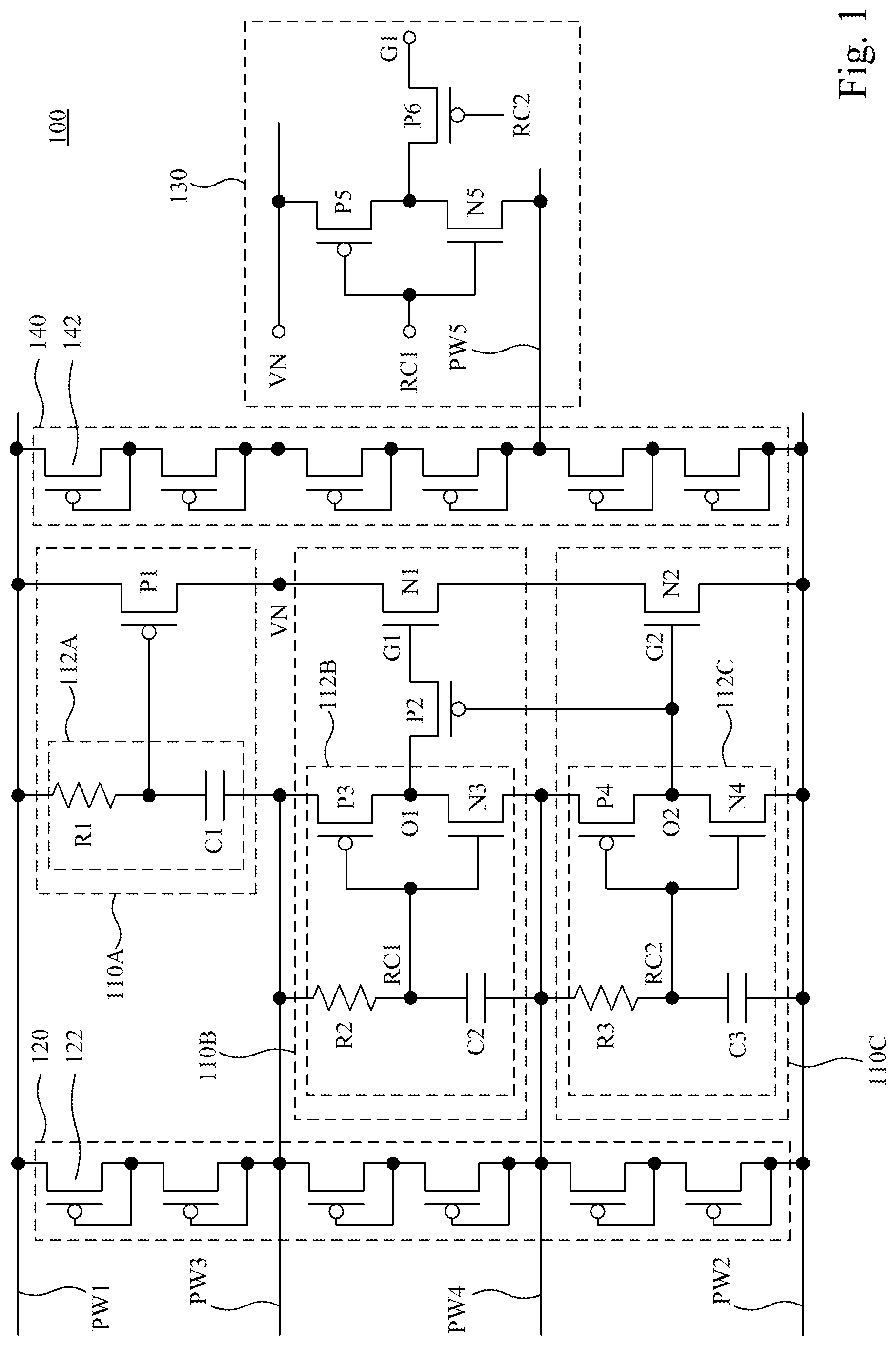
is a schematic diagram of an ESD protection circuit 100 according to one embodiment of the present disclosure. The ESD protection circuit 100 is coupled between the power line PW 1 and power line PW 2 . The ESD protection circuit 100 is configured to form a short circuit between the power line PW 1 and power line PW 2 during the ESD event so that a discharge path is provided to the ESD current between the power line PW 1 and the power line PW 2 . In some embodiments, the power line PW 1 , the power line PW 2 and ESD protection circuit 100 are peripheral circuits of a chip (not shown), and the power line PW 1 and the power line PW 2 are respectively configured to provide an operation voltage (e.g., 5V) and a ground voltage to an internal circuit of the chip. Therefore, the ESD protection circuit 100 is able to protect the electronic components (not shown) in the chip coupled between the power line PW 1 and the power line PW 2 when the ESD event occurs. The ESD protection circuit 100 includes a plurality of ESD clamping circuits 110 A- 110 C, a bias circuit 120 , a shunt circuit 130 , and a bias circuit 140 . The structure and operation of the ESD clamping circuits 110 A- 110 C and the bias circuit 120 are described below.
Structurally, the ESD clamping circuits 110 A- 110 C respectively include a transistor P 1 , a transistor N 1 , and a transistor N 2 , in which the transistor P 1 , the transistor N 1 and the transistor N 2 are coupled in series between the power line PW 1 and the power line PW 2 in this order. In detail, a first terminal of the transistor P 1 and a second terminal of the transistor P 1 are coupled with the power line PW 1 and a node VN, respectively. A first terminal of the transistor N 1 and a second terminal of the transistor N 1 are coupled with the node VN and a first terminal of the transistor N 2 , respectively. A second terminal of the transistor N 2 is coupled with the power line PW 2 .
The ESD clamping circuit 110 A further includes a driving circuit 112 A. The driving circuit 112 A includes a resistor R 1 and a capacitor C 1 , in which the resistor R 1 is coupled between the power line PW 1 and a control terminal of the transistor P 1 . And the capacitor C 1 is coupled between the control terminal of the transistor P 1 and a power line PW 3 . In other words, the driving circuit 112 A is configured to control the transistor P 1 according to the voltage of the power line PW 1 and the voltage of the power line PW 3 .
The ESD clamping circuit 1108 further includes a driving circuit 112 B and a transistor P 2 , in which the driving circuit 112 B includes a resistor R 2 , a capacitor C 2 , and a transistor P 3 and a transistor N 3 that form an inverter. The resistor R 2 is coupled between the power line PW 3 and a node RC 1 . The capacitor C 2 is coupled between the node RC 1 and a power line PW 4 . A first terminal of the transistor P 3 and a second terminal of the transistor P 3 are coupled with the power line PW 3 and a node O 1 , respectively. A first terminal of the transistor N 3 and a second terminal of the transistor N 3 are coupled with the node O 1 and the power line PW 4 , respectively, and a control terminal of the transistor P 3 and a control terminal of the transistor N 3 are coupled with the node RC 1 . The node O 1 may be regarded as the output node of the inverter composed of the transistor P 3 and the transistor N 3 . The first terminal of the transistor P 2 , the second terminal of the transistor P 2 and the control terminal of the transistor P 2 are coupled with a control terminal of the transistor N 1 (hereinafter referred to as a node G 1 ), the node O 1 and a control terminal of the transistor N 2 (hereinafter referred to as a node G 2 ), respectively. In other words, the driving circuit 112 B is configured to control the transistor N 1 according to the voltage of the power line PW 3 and the voltage of the power line PW 4 .
The ESD clamping circuit 110 C further includes a driving circuit 112 C. The driving circuit 112 C includes a resistor R 3 , a capacitor C 3 , and a transistor P 4 and a transistor N 4 that form an inverter. The resistor R 3 is coupled between the power line PW 4 and a node RC 2 . The capacitor C 3 is coupled between the node RC 2 and the power line PW 2 . A first terminal of the transistor P 4 and a second terminal of the transistor P 4 are coupled with the power line PW 4 and a node O 2 , respectively. A first terminal of the transistor N 4 and a second terminal of the transistor N 4 are coupled with the node O 2 and the power line PW 2 , respectively, and a control terminal of the transistor P 4 and a control terminal of the transistor N 4 are coupled with the node RC 2 . The node O 2 may be regarded as the output node of the inverter composed of the transistor P 4 and the transistor N 4 . In other words, the driving circuit 112 C is configured to control the transistor N 2 according to the voltage of the power line PW 2 and the voltage of the power line PW 4 .
The bias circuit 120 is configured to divide a voltage between the first power line PW 1 and the second power line PW 2 to provide at least one reference voltage (e.g., the voltage of the power line PW 3 or the voltage of the power line PW 4 ) to each of the ESD clamping circuits 110 A- 110 C. As mentioned above, the ESD clamping circuits 110 A- 110 C control the transistor P 1 , the transistor N 1 , and the transistor N 2 , respectively, by using these reference voltages.
In detail, the bias circuit 120 includes a plurality of diode-connected transistors 122 coupled in series between the power line PW 1 and the power line PW 2 . Part of the diode-connected transistors 122 are coupled in series between the power line PW 1 and the power line PW 3 , another part of the diode-connected transistors 122 are coupled in series between the power line PW 3 and the power line PW 4 , and the other of the multiple diode-connected transistors 122 are coupled in series between the power line PW 4 and the power line PW 2 . Therefore, the voltage of the power line PW 1 is greater than the voltage of the power line PW 3 , the voltage of the power line PW 3 is greater than the voltage of the power line PW 4 , and the voltage of the power line PW 4 is greater than the voltage of the power line PW 2 . In some embodiments, the voltages of the power lines PW 1 , PW 3 , PW 4 , and PW 2 are 5 V, 3.3 V, 1.8 V, and 0 V, respectively, but this disclosure is not limited thereto. The number of the diode-connected transistors 122 of the bias circuit 120 coupled between any two of the power lines PW 1 -PW 4 is only an exemplary embodiment, and in some embodiments can be adjusted according to actual requirements. In some embodiments, the bias circuit 120 includes a plurality of diodes, a plurality of resistors, a plurality of diode-connected transistors 122 or any combination of the above that are coupled in series between the power line PW 1 and the power line PW 2 .
Outside the period of an ESD event (i.e., under a normal operating condition), the output voltages from the inverters of the ESD clamping circuits 110 A- 110 C can switch off the transistor P 1 , the transistor N 1 and the transistor N 2 (transistor P 2 is in a conducting state), and thereby maintaining the power line PW 1 and the power line PW 2 insulated from each other. In this situation, the output voltages from the inverters of the ESD clamping circuits 110 A- 110 C are around 3.3 V, 1.8 V, and 0 V, respectively, in some embodiments.
On the other hand, during the period of the ESD event, the ESD surge raises the voltage of the power line PW 1 , the voltage of the power line PW 3 and the voltage of the power line PW 4 . Therefore, the ESD clamping circuits 110 A- 110 C conduct the transistor P 1 , the transistor N 1 and the transistor N 2 to drain the ESD current to the power line PW 2 . In some embodiments, the negative ESD current can flow from the power line PW 2 to the power line PW 1 through a P-type substrate and an N-type well (not shown) of the transistor P 1 .
The structure and operation of the shunt circuit 130 and the bias circuit 140 are described below. Structurally, the shunt circuit 130 includes a transistor P 5 and a transistor N 5 that composes the inverter, and includes a transistor P 6 . An input terminal, an output terminal, a positive power terminal and a negative power terminal of the inverter composed of the transistor P 5 and the transistor N 5 are coupled with the node RC 1 , a first terminal of the transistor P 6 , the node VN and a power line PW 5 , respectively. A second terminal and a control terminal of the transistor P 6 are coupled with the node G 1 and the node RC 2 , respectively.
The bias circuit 140 includes a plurality of diode-connected transistors 142 coupled in series between the power line PW 1 and the power line PW 2 . In detail, some of the diode-connected transistors 142 are coupled between the power line PW 1 and the power line PW 5 , and the others are coupled between the power line PW 5 and the power line PW 2 . In some embodiments, a voltage (e.g., 1.8 V) of the power line PW 5 is close to the voltage of the power line PW 4 . The number of the diode-connected transistors 142 of the bias circuit 140 between the power line PW 1 and the power line PW 2 is only an exemplary embodiment, and in some embodiments can be adjusted according to actual requirements. In some embodiments, the bias circuit 140 can include a plurality of diodes, a plurality of resistors, a plurality of diode-connected transistors 142 or any combination of the above that are coupled in series between the power line PW 1 and the power line PW 2 .
Outside the period of the ESD event (i.e., under the normal operating condition), the transistor P 5 and the transistor P 6 are kept being switched off so that the first terminal (i.e., the node VN) and the control terminal (i.e., the node G 1 ) of the transistor N 1 are set to be insulated from each other. On the other hand, during the ESD event, part of the ESD current will be transmitted to the node G 1 through the node VN, the transistor P 5 , and the transistor P 6 , and can be further transmitted from the node G 1 to the node G 2 through the transistor P 2 , the transistor N 3 , the power line PW 4 and the transistor P 4 .
In other words, during the period of the ESD event the shunt circuit 130 raises the voltages of the nodes G 1 and G 2 to increase the conduction degree of the transistor N 1 and the transistor N 2 , so as to ensure the discharging capacity to the ESD current of the serial structure of the transistor P 1 , the transistor N 1 , and the transistor N 2 . In addition, the transistor P 2 is switched from the switched-on state to the switched-off state after the voltages of the nodes G 1 and G 2 are raised, so as to prevent the voltage of the node G 1 from being pulled down by the transistor N 3 . In some embodiments that the transistor N 1 is easier to be conducted due to manufacturing process factors, the transistor P 2 can be omitted, that is, the node O 1 can be directly coupled to the node G 1 .
As can be appreciated from the above, besides the reliable ESD protection capability, the source-drain voltage, the gate-drain voltage, and the gate-source voltage of each transistor in the ESD protection circuit 100 are at lower levels (e.g., none of them exceed 1.8 V) due to the series structure including the transistor P 1 , the transistor N 1 and the transistor N 2 and due to the appropriate voltages provided by the power line PW 3 and the power line PW 4 , so that the ESD protection circuit 100 is applicable to an advanced manufacturing process of lower voltage endurance.
is a schematic diagram of an ESD protection circuit 200 according to one embodiment of the present disclosure. The ESD protection circuit 200 in is similar to the ESD protection circuit 100 in , so the following only explains the differences in detail. The ESD protection circuit 200 replaces the ESD clamping circuit 110 C in by an ESD clamping circuit 210 C, and includes an ESD detection circuit 220 configured to drive the ESD clamping circuit 210 C.
Structurally, the ESD clamping circuit 210 C includes a transistor N 2 and a driving circuit 212 C, in which the driving circuit 212 C includes a transistor P 4 and a transistor N 4 that compose an inverter. Control terminals of the transistor P 4 and the transistor N 4 are coupled with the ESD detection circuit 220 by the node RC 2 . The ESD detection circuit 220 includes a transistor P 7 and a transistor N 6 composing an inverter, a plurality of diodes 222 , and a resistor R 4 . The plurality of diodes 222 are coupled in series between the power line PW 1 and the control terminals of the transistor P 7 and the transistor N 6 . The resistor R 4 is coupled between the power line PW 2 and the control terminals of the transistor P 7 and the transistor N 6 . A first terminal of the transistor P 7 and a second terminal of the transistor P 7 are coupled with the power line PW 4 and the node RC 2 , respectively. A first terminal of the transistor N 6 and a second terminal of the transistor N 6 are coupled with the node RC 2 and the power line PW 2 , respectively. In other words, the plurality of diodes 222 and the resistor R 4 form a bias circuit, and this bias circuit is configured to set the voltage of an input terminal of the inverter composed of the transistor P 7 and the transistor N 6 . In some embodiments, the plurality of diodes 222 and the resistor R 4 can be replaced by a plurality of diode-connected transistors, a plurality of resistors, a plurality of diodes, or any combination of the above that are coupled in series.
In operation, the ESD detection circuit 220 is configured to compare the voltage of the power line PW 1 with a voltage threshold value (e.g., 7 V). If the voltage of the power line PW 1 is greater than the voltage threshold value, the ESD detection circuit 220 controls the ESD clamping circuit 210 C to conduct the transistor N 2 . On the contrary, if the voltage of the power line PW 1 is lower than or equal to the voltage threshold value, the ESD detection circuit 220 controls the ESD clamping circuit 210 C to switch off the transistor N 2 .
In detail, the voltage threshold value can be determined by the number of diodes 222 coupled in series and the resistance of the resistor R 4 . When a surge voltage higher than the voltage threshold value occurs on the power line PW 1 during the period of the ESD event, the inverter formed by the transistor P 7 and the transistor N 6 outputs a voltage equivalent to logic 0 to the node RC 2 , so that the voltage of the node G 2 is equivalent to logic 1 to conduct the transistor N 2 . On the other hand, outside the period of the ESD event period, as long as the voltage of the power line PW 1 is lower than or equal to the voltage threshold value, the inverter formed by the transistor P 7 and the transistor N 6 outputs a voltage equivalent to logic 1 to the node RC 2 , so that the voltage of the node G 2 is equivalent to logic 0 to switch off the transistor N 2 .
By the above operation, the ESD protection circuit 200 of is capable of preventing the internal circuit of the chip to be protected (not shown) from burning out or malfunctioning when a hot plug event occurs. In detail, although the power line PW 1 generates a surge voltage in both the period of the ESD event and a period of the hot plug event, by designing an appropriate voltage threshold value, the ESD protection circuit 200 is capable of distinguishing between the ESD event and the hot plug event. Therefore, the ESD protection circuit 200 would not mistakenly short the internal circuit of the chip to the power line PW 2 (e.g., the ground line) due to the hot plug event, so as to avoid the internal circuit of the chip from burning. In addition, the ESD protection circuit 200 would not mistakenly short the power line PW 1 to the power line PW 2 due to the hot plug event, so that the voltage change of the power line PW 1 due to the hot plug event can be transmitted to the internal circuit of the chip, ensuring that the internal circuit of the chip is capable of detecting the hot plug event correctly.
In some embodiments, the bias circuit 120 of the can be omitted and other peripheral circuits of the chip may provide voltages to the power line PW 3 and the power line PW 4 . In other embodiments, the bias circuit 140 in can be omitted, and other peripheral circuits of the chip may provide a voltage to the power line PW 5 .
In the various above-mentioned embodiments, the transistors P 1 -P 6 in and can be implemented by P-type transistors, and the transistors N 1 -N 5 can be implemented by N-type transistors, but the present disclosure is not limited thereto. In some embodiments, the doping type of each of the transistor P 1 , the transistor N 1 , and the transistor N 2 can be determined according to actual design requirements, and the circuit structures of the driving circuits 112 A- 112 C can be correspondingly adjusted. For example, in an embodiment that the N-type transistor N 1 is replaced by a P-type transistor, the inverter in the driving circuit 112 B can be omitted. In an embodiment that the N-type transistor N 2 is replaced by a P-type transistor, the inverter in the driving circuit 112 C or the driving circuit 212 C can be omitted. In an embodiment that the P-type transistor P 1 is replaced by an N-type transistor, an inverter can be added to the driving circuit 112 A. The following is a detailed description of an embodiment implemented the P-type transistor P 1 is replaced to an N-type transistor in .
is a schematic diagram of an ESD protection circuit 300 according to one embodiment of the present disclosure. The ESD protection circuit 300 in is similar to the ESD protection circuit 200 in , so the following only explains the differences in detail. The ESD protection circuit 300 replaces the ESD clamping circuit 110 A in by an ESD clamping circuit 310 A, in which the ESD clamping circuit 310 A includes an N-type transistor N 7 and a driving circuit 312 A. The transistor N 7 is coupled between the power line PW 1 and the node VN. The driving circuit 312 A includes a resistor R 1 , a capacitor C 1 , and a transistor P 8 and a transistor N 8 that form an inverter. The resistor R 1 is coupled between the power line PW 1 and the node RC 3 . The capacitor C 1 is coupled between the node RC 3 and the power line PW 3 . An input terminal, an output terminal, a positive power terminal and a negative power terminal of the inverter composed of the transistor P 8 and the transistor N 8 are coupled with the node RC 3 , a control terminal of the transistor N 7 , the power line PW 1 and the power line PW 3 , respectively. The components and the connection relationship of the ESD clamping circuit 310 A in are also applicable to the embodiment of . That is, the ESD clamping circuit 110 A in may be replaced by the ESD clamping circuit 310 A in . For the sake of brevity, those descriptions are omitted.
To sum up, the ESD protection circuits 100 - 300 effectively reduce the voltage differences between the terminals of the transistors, through the series structure of the transistors (e.g., the series structure of the transistor P 1 , the transistor N 1 and the transistor N 2 ) and the power lines PW 1 -PW 4 having the voltages in a descending order, so that the ESD protection circuits 100 - 300 are applicable to an advanced process having relatively lower voltage endurance. In addition, through the operation of the shunt circuit 130 , the ESD protection circuits 100 - 300 solve the problem that the series structure of the transistors may have a poor discharge capacity to the ESD current. Moreover, through the operation of the ESD detection circuit 220 , the ESD protection circuits 100 - 300 also can prevent the internal circuit of the chip from burning out when a hot plug event occurs.
Certain terms are used throughout the description and the claims to refer to particular components. One skilled in the art appreciates that a component may be referred to as different names. This disclosure does not intend to distinguish between components that differ in name but not in function. In the description and in the claims, the term “comprise” is used in an open-ended fashion, and thus should be interpreted to mean “include, but not limited to.” The term “couple” is intended to compass any indirect or direct connection. Accordingly, if this disclosure mentioned that a first device is coupled with a second device, it means that the first device may be directly or indirectly connected to the second device through electrical connections, wireless communications, optical communications, or other signal connections with/without other intermediate devices or connection means.
In addition, the singular forms “a,” “an,” and “the” herein are intended to comprise the plural forms as well, unless the context clearly indicates otherwise.
Other embodiments of the present disclosure will be apparent to those skilled in the art from consideration of the specification and practice of the present disclosure disclosed herein. It is intended that the specification and examples be considered as exemplary only, with a true scope and spirit of the present disclosure being indicated by the following claims.
Figures (3)
Citations
This patent cites (9)
- US9048655
- US20080049365
- US20130182356
- US20130265676
- US20200266187
- US20210257353
- US20230009740
- US217641333
- US115274649