Abstract
A semiconductor device includes a light-emitting element, a light-receiving element, a switching element, an input-side terminal, an output-side terminal, and a resin layer. The light-emitting element, the light-receiving element and the switching element are provided at the front side of the resin layer. The light-receiving element and the switching element are arranged in a first direction along the front side of the resin layer. The switching element is electrically connected to the light-receiving element. The light-receiving element is provided between the light-emitting element and the resin layer. The input-side and output-side terminals are provided at the backside of the resin layer. The input-side terminal is electrically connected to the light-emitting element. The output-side terminal is electrically connected to the switching element. At least one of the input-side or output-side terminals includes a portion overlapping the light-emitting element in a second direction from the resin layer to the light-emitting element.
Claims (16)
1. A semiconductor device, comprising: a light-emitting element; a light-receiving element optically coupled with the light-emitting element; a first switching element electrically connected to the light-receiving element; a second switching element electrically connected to the light-receiving element and the first switching element; a first input-side terminal electrically connected to the light-emitting element; a second input-side terminal apart from the first input-side terminal, the second input-side terminal being electrically connected to the light-emitting element; a first output-side terminal electrically connected to the first switching element; a second output-side terminal apart from the first output-side terminal, the second output-side terminal being electrically connected to the second switching element; a first resin layer having a front side and a backside opposite to the front side, the light-emitting element, the light-receiving element, and the first and second switching elements being provided at the front side of the first resin layer, the light-receiving element being provided between the light-emitting element and the first resin layer, the light-receiving element and each of the first and second switching elements being arranged in a first direction along the front side, the first and second input-side terminals and the first and second output-side terminals being provided at the backside of the first resin layer, the first and second input-side terminals being apart in the first direction from the first and second output-side terminals, the light-receiving element being provided, via the first resin layer, on edge portions of the first output-side terminal and the second output-side terminal; and a second resin layer sealing the light-emitting element, the light-receiving element, and the first and second switching elements at the front side of the first resin layer.
11. A semiconductor device, comprising: a light-emitting element; a light-receiving element optically coupled with the light-emitting element; a switching element electrically connected to the light-receiving element a first metal plate electrically connected to the light emitting element by a metal wire, the first metal plate having a front surface and a back surface opposite to the front surface, the metal wire being bonded to the front surface of the first metal plate; a second metal plate having a front surface and a back surface opposite to the front surface, the switching element being provided on the front surface of the second metal plate and electrically connected to the second metal plate; a first resin layer provided between the first metal plate and the second metal plate, the first resin layer having a front surface and a back surface opposite to the front surface, the back surface of the first resin layer being flush and aligned with the back surfaces of the first and second metal plates, the light-receiving element being bonded to the front surface of the first resin layer, the light-emitting element being provided on the light-receiving element; and a second resin layer covering the light emitting element, the light receiving element, the switching element, the front surface of the first resin layer, the front surface of the first metal plate, and the front surface of the second metal plate.
Show 14 dependent claims
2. The device according to claim 1 , further comprising: a first bonding pad provided at the front side of the first resin layer and electrically connected to the light-emitting element via a first metal wire; a first via contact extending through the first resin layer and electrically connecting the first bonding pad and the first input-side terminal; a second bonding pad provided at the front side of the first resin layer and electrically connected to the light-emitting element via a second metal wire; a second via contact extending through the first resin layer and electrically connecting the second bonding pad and the second input-side terminal; a first mount pad provided between the first resin layer and the first switching element and electrically connected to the first switching element; a third via contact extending through the first resin layer and electrically connecting the first switching element and the first output-side terminal; a second mount pad provided between the first resin layer and the second switching element and electrically connected to the second switching element; and a fourth via contact extending through the first resin layer and electrically connecting the second switching element and the second output-side terminal.
3. The device according to claim 2 , wherein the light-emitting element includes a back surface connected to the light-receiving element, a front surface at a side opposite to the back surface, and first and second electrodes provided on the front surface, and the first and second metal wires are bonded to the first and second electrodes, respectively, on the front surface of the light-emitting element.
4. The device according to claim 2 , wherein the second resin layer covers the first and second metal wires and the first and second bonding pads.
5. The device according to claim 1 , wherein the first resin layer has a thickness of not more than 50 micrometers in a second direction perpendicular to the front side of the first resin layer.
6. The device according to claim 1 , further comprising: a third mount pad provided between the first resin layer and the light-receiving element.
7. The device according to claim 1 , further comprising: a third resin layer sealing the light-emitting element on the light-receiving element, wherein the second resin layer covers the third resin layer.
8. The device according to claim 1 , wherein each of the first and second switching elements is a MOS transistor, the MOS transistor includes a source electrode, a drain electrode, and a gate electrode, the light-receiving element includes a first couple of electrodes electrically connected respectively to the source electrodes of the first and second switching elements and a second couple of electrodes electrically connected respectively to the gate electrodes of the first and second switching elements via metal wires, and each of the first and second output-side terminals is electrically connected to the drain electrodes of the first and second switching elements.
9. The device according to claim 8 , wherein each of the first and second switching elements includes: a back surface facing the first resin layer; and a front surface at a side opposite to the back surface of the switching element, the source electrode and the gate electrode being provided on each front surface of the first and second switching elements, the drain electrode being provided on each back surface of the first and second switching elements, and the light-receiving element includes: a back surface facing the first resin layer; and a front surface at a side opposite to the back surface of the light-receiving element, the front surface of the light-receiving element including a first region connected to the light-emitting element and a second region other than the first region, the light-receiving element including the first and second couples of electrodes on the second region.
10. The device according to claim 1 , wherein the light-receiving element is provided, via the first resin layer, on edge portions of the first input-side terminal, the second input-side terminal, the first output-side terminal, and the second output-side terminal.
12. The device according to claim 11 , further comprising: a third resin layer covering the light-emitting element on the light-receiving element, the third resin layer being provided between the second resin layer and the light-receiving element.
13. The device according to claim 11 , wherein the second metal plate includes a trench provided at the front surface of the second metal plate.
14. The device according to claim 11 , wherein the first resin layer has a layer thickness in a first direction perpendicular to the back surface of the first resin layer, the layer thickness of the first resin layer being greater than thicknesses of the first and second metal plates in the first direction.
15. The device according to claim 11 , further comprising: a third metal plate away from the first metal plate, the third metal plate being provided next to the first metal plate in a second direction along the back surface of the first metal plate; a fourth metal plate away from the second metal plate, the fourth metal plate being provided next to the second metal plate in the second direction, the first resin layer extending between the third metal plate and the fourth metal plate, between the first metal plate and the third metal plate, and between the second metal plate and the fourth metal plate, the back surface of the first resin layer being flush and aligned with a back surface of the third metal plate and a back surface of the fourth metal plate; and a second switching element provided on a front surface of the fourth metal plate, the second switching element being electrically connected to the light-receiving element, the switching element and the fourth metal plate, the second resin layer further covering the front surface of the third metal plate, the front surface of the fourth metal plate, and the second switching element.
16. The device according to claim 11 , wherein the switching element hash a back surface bonded to the front surface of the second metal plate, and the back surface of the switching element has an area less than the front surface of the second metal plate.
Full Description
Show full text →
CROSS-REFERENCE TO RELATED APPLICATIONS
This application is based upon and claims the benefit of priority from Japanese Patent Application No. 2020-156329, filed on Sep. 17, 2020; the entire contents of which are incorporated herein by reference.
FIELD
Embodiments relate to a semiconductor device.
BACKGROUND
A semiconductor device includes a semiconductor chip sealed by a resin on a glass epoxy substrate. In such a semiconductor device, terminals that connect the semiconductor chip to an external circuit are provided at the back surface of the glass epoxy substrate. Therefore, intermediate interconnects that electrically connect the semiconductor chip and the terminals are provided inside the glass epoxy substrate. On the other hand, to operate the semiconductor chip at a high speed, it is desirable to shorten the intermediate interconnects electrically connecting the semiconductor chip and the terminals.
BRIEF DESCRIPTION OF THE DRAWINGS
is a schematic cross-sectional view showing a semiconductor device according to a first embodiment;
is a schematic view showing the semiconductor device according to the first embodiment;
A and 3 B are schematic plan views showing the input-side terminals and the output-side terminals of the semiconductor device according to the first embodiment;
A is a schematic cross-sectional view showing a semiconductor device according to a modification of the first embodiment;
B is a schematic plan view showing the semiconductor device according to the modification of the first embodiment;
A is a schematic cross-sectional view showing a semiconductor device according to another modification of the first embodiment;
B is a schematic plan view showing the semiconductor device according to said another modification of the first embodiment;
is a schematic cross-sectional view showing a semiconductor device according to a second embodiment;
A and 7 B are schematic plan views showing the semiconductor device according to the second embodiment; and
A to 8 E are schematic cross-sectional views showing manufacturing processes of the semiconductor device according to the second embodiment.
DETAILED DESCRIPTION
According to one embodiment, a semiconductor device includes a light-emitting element, a light-receiving element, at least a switching element, at least an input-side terminal, at least an output-side terminal, a first resin layer, and a second resin layer. The light-receiving element is optically coupled with the light-emitting element. The switching element is electrically connected to the light-receiving element. The input-side terminal is electrically connected to the light-emitting element. The output-side terminal is electrically connected to the switching element. The first resin layer includes a front side and a backside opposite to the front side. The light-emitting element, the light-receiving element and the switching element are provided at the front side. The light-receiving element is provided between the light-emitting element and the first resin layer. The light-receiving element and the switching element are arranged in a first direction along the front side of the first resin layer. The input-side terminal and the output-side terminal are provided at the backside of the first resin layer. The input-side terminal is apart from the output-side terminal. At least one of the input-side terminal or the output-side terminal includes a portion overlapping the light-receiving element in a second direction from the first resin layer toward the light-emitting element. The second resin layer seals the light-emitting, light-receiving, and switching elements at the front side of the first resin layer.
Embodiments will now be described with reference to the drawings. The same portions inside the drawings are marked with the same numerals; a detailed description is omitted as appropriate; and the different portions are described. The drawings are schematic or conceptual; and the relationships between the thicknesses and widths of portions, the proportions of sizes between portions, etc., are not necessarily the same as the actual values thereof. The dimensions and/or the proportions may be illustrated differently between the drawings, even in the case where the same portion is illustrated.
There are cases where the dispositions of the components are described using the directions of XYZ axes shown in the drawings. The X-axis, the Y-axis, and the Z-axis are orthogonal to each other. Hereinbelow, the directions of the X-axis, the Y-axis, and the Z-axis are described as an X-direction, a Y-direction, and a Z-direction. Also, there are cases where the Z-direction is described as upward and the direction opposite to the Z-direction is described as downward.
First Embodiment
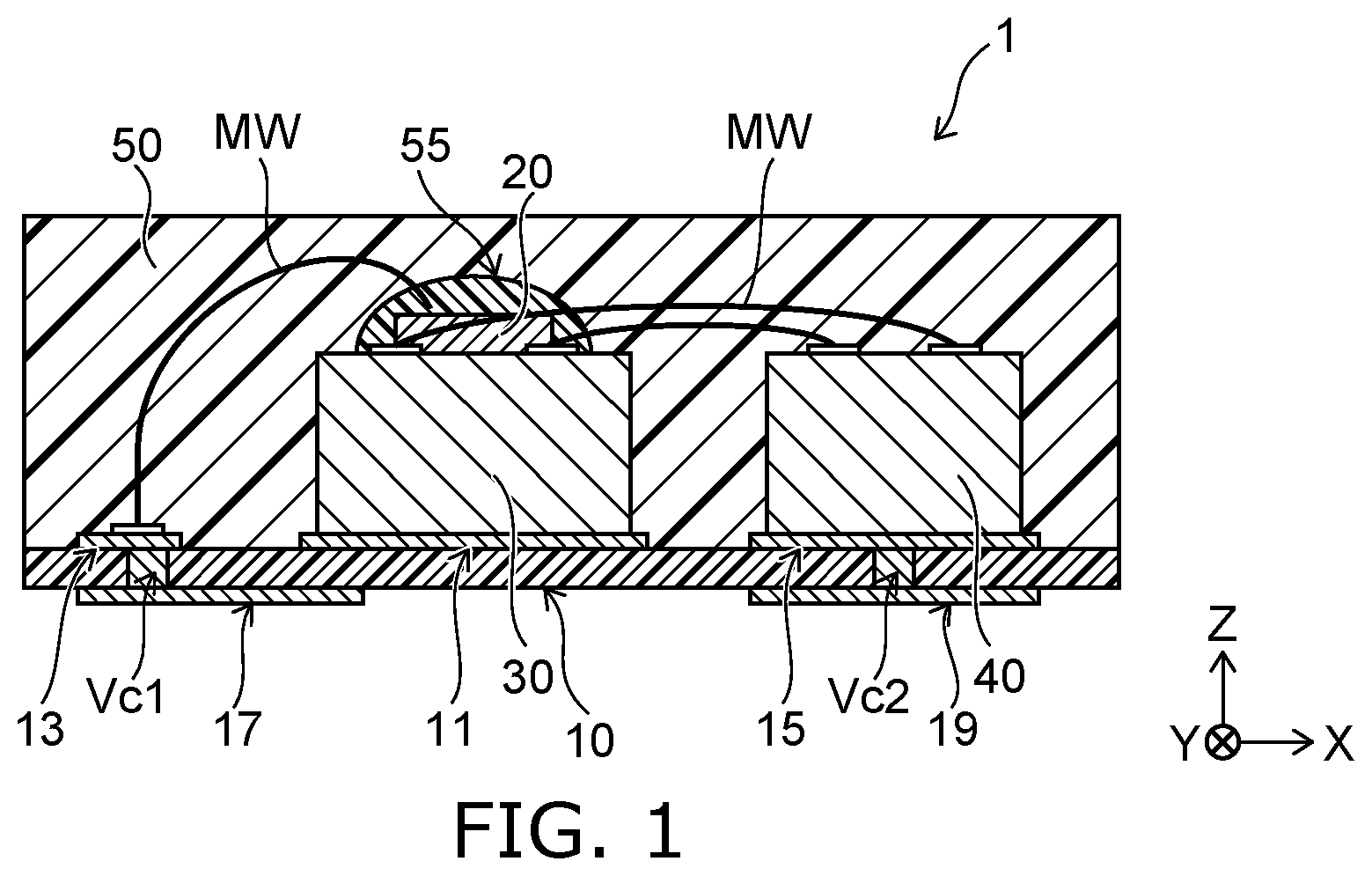
is a schematic cross-sectional view showing a semiconductor device 1 according to a first embodiment. The semiconductor device 1 is, for example, a photo-relay.
The semiconductor device 1 includes a light-emitting element 20 , a light-receiving element 30 , and a switching element 40 . The light-emitting element 20 is, for example, a light-emitting diode. Moreover, the light-receiving element 30 includes, for example, multiple photodiodes provided on a silicon substrate. The switching element 40 is, for example, a MOS (Metal Oxide Semiconductor) transistor.
As shown in , the light-emitting element 20 is mounted on the light-receiving element 30 . For example, the light-emitting element 20 is bonded on the front surface of the light-receiving element 30 via a transparent adhesive layer. For example, the light-emitting element 20 emits light from the backside and is mounted with the back surface toward the light-receiving element 30 .
The light-receiving element 30 and the switching element 40 are mounted on a resin layer 10 . The resin layer 10 is located at the backside of the light-receiving element 30 and the backside of the switching element 40 . The resin layer 10 is, for example, a polyimide layer. The thickness in the direction from the back surface toward the front surface of the resin layer 10 (in the Z-direction) is, for example, not more than 50 micrometers.
A mount pad 11 , a bonding pad 13 , and a mount pad 15 are provided on the front surface of the resin layer 10 . The mount pad 11 , the bonding pad 13 , and the mount pad 15 are apart from each other. For example, the mount pad 11 is located between the bonding pad 13 and the mount pad 15 . The mount pad 11 , the bonding pad 13 , and the mount pad 15 include copper, for example.
The light-emitting element 20 is electrically connected to the bonding pad 13 via a metal wire MW. For example, the light-receiving element 30 is mounted on the mount pad 11 via an adhesive layer (not illustrated) such as a die attach film, etc. For example, the switching element 40 is mounted on the mount pad 15 via a conductive paste (not illustrated).
The mount pad 11 is located between the resin layer 10 and the light-receiving element 30 . The mount pad 15 is located between the resin layer 10 and the switching element 40 .
The light-emitting element 20 is sealed by a resin layer 55 on the light-receiving element 30 . The resin layer 55 includes, for example, silicone. The resin layer 55 is formed on the light-receiving element 30 by, for example, potting.
The light-receiving element 30 and the switching element 40 are sealed by a resin layer 50 on the resin layer 10 . The resin layer 50 covers the resin layer 55 . The resin layer 50 is, for example, a polyimide layer or an epoxy resin.
An input-side terminal 17 and an output-side terminal 19 are provided on the back surface of the resin layer 10 . The input-side terminal 17 and the output-side terminal 19 are apart from each other. The input-side terminal 17 faces the bonding pad 13 with a portion of the resin layer 10 interposed. The output-side terminal 19 faces the mount pad 15 with another portion of the resin layer 10 interposed.
The resin layer 10 includes a via contact Vc 1 provided between the bonding pad 13 and the input-side terminal 17 , and a via contact Vc 2 provided between the mount pad 15 and the output-side terminal 19 . The input-side terminal 17 is electrically connected to the bonding pad 13 by the via contact Vc 1 that extends through the resin layer 10 in the Z-direction. The output-side terminal 19 is electrically connected to the mount pad 15 by the via contact Vc 2 that extends through the resin layer 10 in the Z-direction.
The light-emitting element 20 is electrically connected to the input-side terminal 17 via the metal wire MW, the bonding pad 13 , and the via contact Vc 1 . The switching element 40 is electrically connected to the output-side terminal 19 via the mount pad 15 and the via contact Vc 2 .
For example, the via contacts Vc 1 and Vc 2 have the same Z-direction lengths as the thickness in the Z-direction of the resin layer 10 . The thickness of the resin layer 10 is not more than 50 μm; and the length of the electrical connection between the bonding pad 13 and the input-side terminal 17 is the length of the via contact Vc 1 . The length of the electrical connection between the switching element 40 and the output-side terminal 19 is the length of the via contact Vc 2 . The parasitic inductance that is caused by the interconnect length inside the resin layer 10 can be reduced thereby, and the semiconductor device 1 can operate at a high speed.
The input-side terminal 17 further includes a portion overlapping the light-receiving element 30 when viewed from the Z-direction. In other words, the resin layer 10 includes a portion positioned between the light-receiving element 30 and a portion of the input-side terminal 17 .
For example, when performing ultrasonic bonding of the metal wires MW to the light-emitting element 20 and the light-receiving element 30 , the ultrasonic waves are absorbed by the resin layer 10 , and there are cases where the intensity of the ultrasonic waves necessary for the bonding is not obtained. Therefore, there are cases where the bonding strength is insufficient, and the reliability of the semiconductor device 1 decreases.
In the configuration of the embodiment, the light-receiving element 30 and a portion of the input-side terminal 17 overlap, and the ultrasonic waves are efficiently transmitted from the input-side terminal 17 to the light-receiving element 30 . The bonding strength of the metal wires MW can be increased thereby, and the reliability of the semiconductor device 1 can be increased.
is a schematic view showing the semiconductor device 1 according to the first embodiment. includes a plan view and an equivalent circuit diagram showing the layout on the front surface of the resin layer 10 .
As shown in , the semiconductor device 1 includes bonding pads 13 a and 13 b and switching elements 40 a and 40 b . The bonding pads 13 a and 13 b are electrically connected respectively to input-side terminals 17 a and 17 b (referring to A ). The switching elements 40 a and 40 b are electrically connected respectively to output-side terminals 19 a and 19 b (referring to B ). In the specification, the bonding pads 13 a and 13 b may be generally referred to as the bonding pad 13 . This is similar for the other components as well.
The light-emitting element 20 includes a first electrode 23 and a second electrode 25 . The first electrode 23 is, for example, a p-electrode. The second electrode 25 is, for example, an n-electrode. The first electrode 23 is electrically connected to the bonding pad 13 a via a metal wire MW 1 . The second electrode 25 is electrically connected to the bonding pad 13 b via a metal wire MW 2 .
The light-receiving element 30 includes, for example, cathode terminals 31 a and 31 b and anode terminals 33 a and 33 b . The switching element 40 a includes, for example, a source electrode 41 a and a gate electrode 43 a . The switching element 40 b includes, for example, a source electrode 41 b and a gate electrode 43 b.
The switching elements 40 a and 40 b are arranged in the Y-direction on the resin layer 10 . In the light-receiving element 30 , the cathode terminal 31 a and the anode terminal 33 a are located at one Y-direction end, and the cathode terminal 31 b and the anode terminal 33 b are located at the other Y-direction end.
The cathode terminal 31 a of the light-receiving element 30 is electrically connected to the source electrode 41 a of the first switching element 40 a via a metal wire MW 3 . The anode terminal 33 a of the light-receiving element 30 is electrically connected to the gate electrode 43 a of the first switching element 40 a via a metal wire MW 4 .
The cathode terminal 31 b of the light-receiving element 30 is electrically connected to the source electrode 41 b of the second switching element 40 b via a metal wire MW 5 . The anode terminal 33 b of the light-receiving element 30 is electrically connected to the gate electrode 43 b of the second switching element 40 b via a metal wire MW 6 .
The source electrode 41 a of the first switching element 40 a is electrically connected to the source electrode 41 b of the second switching element 40 b via a metal wire MW 7 .
In the semiconductor device 1 , for example, a current signal is input to the light-emitting element 20 from the input-side terminals 17 a and 17 b (referring to A ) via the bonding pads 13 a and 13 b and the metal wires MW 1 and MW 2 . The light-emitting element 20 radiates, toward the light-receiving element 30 , an optical signal corresponding to the input current signal.
The light-receiving element 30 includes, for example, a photodiode array 30 a and a control circuit 30 b . The photodiode array 30 a receives the optical signal of the light-emitting element 20 and outputs a voltage signal to the control circuit 30 b . The control circuit 30 b outputs a voltage signal between the gate and source of the first switching element 40 a via the cathode terminal 31 a and the anode terminal 33 a . The control circuit 30 b also outputs a voltage signal between the gate and source of the second switching element 40 b via the cathode terminal 31 b and the anode terminal 33 b.
The photodiode array 30 a receives the optical signal radiated from the light-emitting element 20 and turns on the first switching element 40 a and the second switching element 40 b by applying a prescribed voltage between the gate and source for each of the first switching element 40 a and the second switching element 40 b . Electrical conduction between the output-side terminal 19 a and the output-side terminal 19 b is caused thereby.
In the embodiment, the parasitic inductance can be reduced between the input-side terminal 17 a and the bonding pad 13 a and between the input-side terminal 17 b and the bonding pad 13 b . Also, the parasitic inductance can be reduced between the first switching element 40 a and the output-side terminal 19 a and between the second switching element 40 b and the output-side terminal 19 b . Thereby, a signal that corresponds to high frequency modulation of the input signal can be output via the first switching element 40 a and the second switching element 40 b.
A and 3 B are schematic plan views showing the input-side terminals and the output-side terminals of the semiconductor device 1 according to the first embodiment. A and 3 B show the input-side terminals 17 a and 17 b and the output-side terminals 19 a and 19 b located on the back surface of the resin layer 10 . The broken line in the drawing illustrates the position of the light-receiving element 30 .
As shown in A , the input-side terminals 17 a and 17 b each include a portion overlapping the light-receiving element 30 when viewed from the Z-direction. Thereby, the light-emitting element 20 and the light-receiving element 30 are linked via the resin layer 10 with the portions of the input-side terminal 17 . Therefore, when bonding the metal wires MW (referring to A ), for example, the ultrasonic waves that are supplied to the bonding balls can be transmitted to the electrodes of the front surface of the light-emitting element 20 (referring to ) and the terminals of the light-receiving element 30 (referring to ); and the metal wires can be securely compression-bonded by the vibration.
In the example shown in B , the input-side terminal 17 b includes a portion overlapping the light-receiving element 30 when viewed from the Z-direction. On the other hand, the input-side terminal 17 a does not overlap the light-receiving element 30 when viewed from the Z-direction. Thus, one of the input-side terminal 17 a or 17 b may overlap the light-receiving element 30 .
A and 4 B are, respectively, a schematic cross-sectional view and a schematic plan view showing a semiconductor device 2 according to a modification of the first embodiment. A is a schematic cross-sectional view of the semiconductor device 2 . B shows the input-side terminals 17 a and 17 b and the output-side terminals 19 a and 19 b located on the back surface of the resin layer 10 . The broken line in the drawing illustrates the position of the light-receiving element 30 .
In the semiconductor device 2 as shown in A , the input-side terminal 17 and the output-side terminal 19 each extend below the light-receiving element 30 along the back surface of the resin layer 10 . In other words, the resin layer 10 includes a portion that is positioned between the input-side terminal 17 and the light-receiving element 30 , and another portion that is positioned between the output-side terminal 19 and the light-receiving element 30 .
As shown in B , the input-side terminals 17 a and 17 b each overlap the light-receiving element 30 when viewed from the Z-direction. Also, the output-side terminals 19 a and 19 b each overlap the light-receiving element 30 when viewed from the Z-direction.
Alternatively, one of the input-side terminal 17 a or 17 b may overlap the light-receiving element 30 when viewed from the Z-direction (referring to B ). Also, one of the output-side terminal 19 a or 19 b may overlap the light-receiving element 30 when viewed from the Z-direction.
A and 5 B are, respectively, a schematic cross-sectional view and a schematic plan view showing a semiconductor device 3 according to another modification of the first embodiment. A is a schematic cross-sectional view of the semiconductor device 3 . B shows the input-side terminals 17 a and 17 b and the output-side terminals 19 a and 19 b located on the back surface of the resin layer 10 . The broken line in the drawing illustrates the position of the light-receiving element 30 .
In the semiconductor device 3 as shown in A , the output-side terminal 19 extends below the light-receiving element 30 along the back surface of the resin layer 10 . In other words, the resin layer 10 includes a portion positioned between the output-side terminal 19 and the light-receiving element 30 .
As shown in B , the input-side terminals 17 a and 17 b do not overlap the light-receiving element 30 when viewed from the Z-direction. The output-side terminals 19 a and 19 b each overlap the light-receiving element 30 when viewed from the Z-direction. Alternatively, one of the output-side terminal 19 a or 19 b may overlap the light-receiving element 30 .
Second Embodiment
is a schematic cross-sectional view showing a semiconductor device 4 according to a second embodiment. The semiconductor device 4 includes a resin layer 60 , an input pad 70 , and an output pad 80 instead of the resin layer 10 , the input-side terminal 17 , and the output-side terminal 19 .
The resin layer 60 is located between the input pad 70 and the output pad 80 . For example, the resin layer 60 , the input pad 70 , and the output pad 80 have thicknesses in the Z-direction of not more than 100 μm. It is favorable for the thickness in the Z-direction of the resin layer 60 to be greater than the thicknesses in the Z-direction of the input pad 70 and the output pad 80 . The resin layer 60 is, for example, a polyimide layer. The input pad 70 and the output pad 80 are metal plates including, for example, copper.
In the example, the light-receiving element 30 is mounted on the resin layer 60 via, for example, a not-illustrated adhesive layer. For example, the light-receiving element 30 may be mounted on a mount pad 63 . The light-emitting element 20 is bonded on the front surface of the light-receiving element 30 via, for example, an adhesive layer (not illustrated) that is transparent to the light radiated from the light-emitting element 20 . The light-emitting element 20 is electrically connected to the input pad 70 via, for example, the metal wire MW.
The switching element 40 is mounted on the output pad 80 via, for example, a conductive paste (not illustrated). The switching element 40 is electrically connected to the light-receiving element 30 via, for example, another metal wire MW.
The light-emitting element 20 is sealed by the resin layer 55 at the front side of the light-receiving element 30 . The light-receiving element 30 and the switching element 40 are sealed by the resin layer 50 on the resin layer 60 and on the output pad 80 . The resin layer 50 covers the resin layer 55 .
In the example, the metal wire MW that is linked to the light-emitting element 20 is directly bonded to the input pad 70 . The switching element 40 is directly mounted to the output pad 80 . The attenuation of the high frequency signal passing through the switching element 40 can be reduced thereby. In other words, the transmission characteristics of the high frequency signal transmitted from the input side to the output side can be improved.
A and 7 B are schematic plan views showing the semiconductor device 4 according to the second embodiment. A is a plan view showing the layout of the front side of the semiconductor device 4 . B is a plan view showing the layout of the backside of the semiconductor device 4 .
As shown in A , the semiconductor device 4 includes input pads 70 a and 70 b , the switching elements 40 a and 40 b , and output pads 80 a and 80 b . The switching elements 40 a and 40 b are mounted respectively on the output pads 80 a and 80 b . The resin layer 60 extends between the input pad 70 a and the input pad 70 b and between the output pad 80 a and the output pad 80 b.
The first electrode 23 of the light-emitting element 20 is electrically connected to the input pad 70 a via the metal wire MW 1 . The second electrode 25 of the light-emitting element 20 is electrically connected to the input pad 70 b via the metal wire MW 2 .
The cathode terminal 31 a of the light-receiving element 30 is electrically connected to the source electrode 41 a of the first switching element 40 a via the metal wire MW 3 . The anode terminal 33 a of the light-receiving element 30 is electrically connected to the gate electrode 43 a of the first switching element 40 a via the metal wire MW 4 .
The cathode terminal 31 b of the light-receiving element 30 is electrically connected to the source electrode 41 b of the second switching element 40 b via the metal wire MW 5 . The anode terminal 33 b of the light-receiving element 30 is electrically connected to the gate electrode 43 b of the second switching element 40 b via the metal wire MW 6 .
The source electrode 41 a of the first switching element 40 a is electrically connected to the source electrode 41 b of the second switching element 40 b via the metal wire MW 7 .
As shown in B , the input pads 70 a and 70 b and the output pads 80 a and 80 b are not covered with the resin layer 60 at the backside.
A method for manufacturing the semiconductor device 4 will now be described with reference to A to 8 E . A to 8 E are schematic cross-sectional views showing manufacturing processes of the semiconductor device 4 according to the second embodiment.
As shown in A , the input pad 70 and the output pad 80 are located on a support plate 100 and are apart from each other. The output pad 80 includes, for example, a trench SG at the front side. For example, the input pad 70 and the output pad 80 are fixed on the support plate via adhesive sheets (not illustrated). The support plate 100 is, for example, a stainless steel plate.
As shown in B , the resin layer 60 is formed in the space between the input pad 70 and the output pad 80 , between the input pads 70 a and 70 b , and between the output pads 80 a and 80 b . For example, the resin layer 60 is formed by molding a resin such as polyimide, etc., at the front side of the support plate 100 , and by subsequently polishing the resin formed on the input pad 70 and the output pad 80 so that the portion of the resin filled between the input pad 70 and the output pad 80 remains. For example, the resin layer 60 is formed by transfer molding or compression molding. The resin layer 60 also may be filled into the space between the input pad 70 and the output pad 80 by using, for example, a dispenser.
As shown in C , the light-receiving element 30 is mounted on the resin layer 60 , and the switching element 40 is mounted on the output pad 80 . The light-receiving element 30 is mounted via, for example, a die attach film (not illustrated) adhered to the backside of the light-receiving element 30 . For example, the switching element 40 is mounted via a conductive paste 45 coated onto the front surface of the output pad 80 . For example, the trench SG prevents the spreading of the conductive paste 45 outside the switching element 40 .
The light-emitting element 20 is bonded on the light-receiving element 30 via, for example, an adhesive (not illustrated) that is transparent to the radiated light. Continuing, by the metal wires MW, the light-emitting element 20 and the input pad 70 are electrically connected and the light-receiving element 30 and the switching element 40 are electrically connected.
As shown in D , the light-emitting element 20 is sealed on the light-receiving element 30 by the resin layer 55 . The resin layer 55 is potted on the light-receiving element 30 by using, for example, a dispenser.
Subsequently, the resin layer 50 that covers the light-emitting element 20 , the light-receiving element 30 , and the switching element 40 is molded. The conductive paste 45 is prevented from spreading outside the switching element 40 by providing the trench SG in the output pad 80 . Thereby, the conductive paste 45 can be prevented from existing between the resin layer 50 and the output pad 80 , and the adhesion between the resin layer 50 and the output pad 80 can be improved.
As shown in E , the support plate 100 is detached after curing the resin layer 50 . The input pad 70 and the output pad 80 are exposed at the backside of the semiconductor device 4 (referring to B ).
While certain embodiments have been described, these embodiments have been presented by way of example only, and are not intended to limit the scope of the inventions. Indeed, the novel embodiments described herein may be embodied in a variety of other forms; furthermore, various omissions, substitutions and changes in the form of the embodiments described herein may be made without departing from the spirit of the inventions. The accompanying claims and their equivalents are intended to cover such forms or modifications as would fall within the scope and spirit of the invention.
Figures (8)
Citations
This patent cites (24)
- US9171969
- US20050029633
- US20050189474
- US20140084305
- US20140284629
- US20140374776
- US20150069423
- US20150262985
- US20150263184
- US20160268241
- US20170012506
- US20170040305
- US20170069610
- US20170176519
- US20170186738
- US20200091367
- US20200194411
- USS54001439
- USH11261102
- US2002217234
- US2010034103
- US2015056531
- US2017022961
- US2017033961