Semiconductor Integrated Circuit Device
Abstract
In an output circuit of a semiconductor integrated circuit device, an output transistor is placed apart from an ESD protection diode connected to an external output terminal, and a protection resistance is placed between them. The protection resistance is formed as a plurality of separate resistance regions, and taps supplying a power supply voltage to a substrate or a well are formed between the resistance regions. Noise applied to the external output terminal is attenuated by the protection resistance before reaching the output transistor and absorbed through the taps.
Claims (7)
1. A semiconductor integrated circuit device provided with an output circuit, the output circuit comprising: an external output terminal; a first output transistor outputting an output signal to the external output terminal; a first electrostatic discharge (ESD) protection diode connected to the external output terminal; and a first protection resistance connected between the first output transistor and the first ESD protection diode,
Show 6 dependent claims
2. The semiconductor integrated circuit device of claim 1 , wherein the first output transistor and the first ESD protection diode are placed apart from each other in a first direction, and the plurality of resistance regions are spaced from each other in a second direction perpendicular to the first direction.
3. The semiconductor integrated circuit device of claim 1 , wherein the first output transistor and the first ESD protection diode are placed apart from each other in a first direction, and the plurality of resistance regions are spaced from each other in the first direction.
4. The semiconductor integrated circuit device of claim 1 , wherein the taps have a fin-structure diffusion region.
5. The semiconductor integrated circuit device of claim 1 , wherein in a single region between the resistance regions, taps supplying a first power supply voltage to a substrate or a well and taps supplying a second power supply voltage different from the first power supply voltage to the substrate or the well are formed.
6. The semiconductor integrated circuit device of claim 1 , wherein the output circuit further comprises: a second output transistor outputting an output signal to the external output terminal; a second ESD protection diode connected to the external output terminal; and a second protection resistance connected between the second output transistor and the second ESD protection diode, the second output transistor and the second ESD protection diode are placed apart from each other, and the second protection resistance is placed between the second output transistor and the second ESD protection diode, as viewed in plan, and the second protection resistance is formed as a plurality of separate second resistance regions, and taps supplying a power supply voltage to a substrate or a well are formed between the second resistance regions.
7. The semiconductor integrated circuit device of claim 1 , wherein the output circuit further comprises: a second output transistor outputting an output signal to the external output terminal; and a second ESD protection diode connected to the external output terminal, the second output transistor is placed adjacent to the first output transistor, and the second ESD protection diode is placed adjacent to the first ESD protection diode, as viewed in plan, and the first protection resistance is placed between the first and second output transistors and the first and second ESD protection diodes.
Full Description
Show full text →
CROSS-REFERENCE TO RELATED APPLICATIONS
This is a continuation of International Application No. PCT/JP2020/039593 filed on Oct. 21, 2020, which claims priority to Japanese Patent Application No. 2019-201491 filed on Nov. 6, 2019. The entire disclosures of these applications are incorporated by reference herein.
BACKGROUND
The present disclosure relates to a semiconductor integrated circuit device in which a core region and an I/O region are placed on a chip, and more particularly to a layout structure of an I/O cell placed in the I/O region.
In a semiconductor integrated circuit device, input/output (I/O) cells are arranged around the core region and, through the I/O cells, input/output of signals from/to the outside of the semiconductor integrated circuit device and supply of power are performed.
With the recent progress to finer semiconductor integrated circuit devices, their resistance against noise is decreasing. In particular, a latch-up phenomenon caused by noise applied from pads in I/O cells has raised a large problem.
Japanese Unexamined Patent Publication No. 2011-96897 discloses a semiconductor integrated circuit device in which a diode is provided as an electrostatic discharge (ESD) protection circuit for an external connection terminal and also a resistive element as a protection resistance is placed between an output transistor and the external connection terminal.
In the configuration disclosed in the cited patent document, the output transistor is protected from ESD by the diode as the ESD protection element and the resistive element. In this configuration, however, occurrence of a latch-up phenomenon caused by noise propagating through a well and a substrate cannot be sufficiently controlled.
An objective of the present disclosure is providing a configuration of a semiconductor integrated circuit device capable of sufficiently controlling the occurrence of the latch-up phenomenon.
SUMMARY
According to the first mode of the present disclosure, in a semiconductor integrated circuit device provided with an output circuit, the output circuit includes: an external output terminal; a first output transistor outputting an output signal to the external output terminal; a first electrostatic discharge (ESD) protection diode connected to the external output terminal; and a first protection resistance connected between the first output transistor and the first ESD protection diode, wherein the first output transistor and the first ESD protection diode are placed apart from each other, and the first protection resistance is placed between the first output transistor and the first ESD protection diode, as viewed in plan, and the first protection resistance is formed as a plurality of separate resistance regions, and taps supplying a power supply voltage to a substrate or a well are formed between the resistance regions.
According to the above mode, the output transistor is placed apart from the first ESD protection diode connected to the external output terminal, and the first protection resistance is placed between them. With this configuration, noise applied to the external output terminal is attenuated by the first protection resistance before reaching the first output transistor. Also, the first protection resistance is formed as a plurality of separate resistance regions, and taps supplying a power supply voltage to a substrate or a well are formed between the resistance regions. With this configuration, noise applied to the external output terminal is absorbed through the taps. It is therefore possible to control propagation of noise that is to be a cause of occurrence of the latch-up phenomenon.
According to the present disclosure, in a semiconductor integrated circuit device, the occurrence of the latch-up phenomenon can be sufficiently controlled.
BRIEF DESCRIPTION OF THE DRAWINGS
is a plan view schematically showing the entire configuration of a semiconductor integrated circuit device according to an embodiment.
is a circuit diagram of an output circuit according to the first embodiment.
shows an example of the planar layout structure of the output circuit according to the first embodiment.
shows an example of the layout structure of an ESD protection diode.
shows an example of the layout structure of an ESD protection diode.
shows an example of the layout structure of a protection resistance.
shows an example of the layout structure of a protection resistance.
shows an example of the layout structure of an output transistor.
shows an example of the layout structure of an output transistor.
shows a view for explaining how to control occurrence of a latch-up phenomenon.
shows another example of the planar layout structure of the output circuit according to the first embodiment.
is a circuit diagram of an output circuit according to the second embodiment.
shows an example of the planar layout structure of the output circuit according to the second embodiment.
A and 14 B show other examples of the planar layout structure of the output circuit according to the second embodiment.
DETAILED DESCRIPTION
Embodiments of the present disclosure will be described hereinafter with reference to the accompanying drawings. It is herein assumed that “VDDIO” and “VSS” refer to power supply voltages or power supplies themselves. It is also assumed that transistors are formed on a P-substrate and an N-well. Note however that transistors may be formed on a P-well and an N-substrate.
First Embodiment
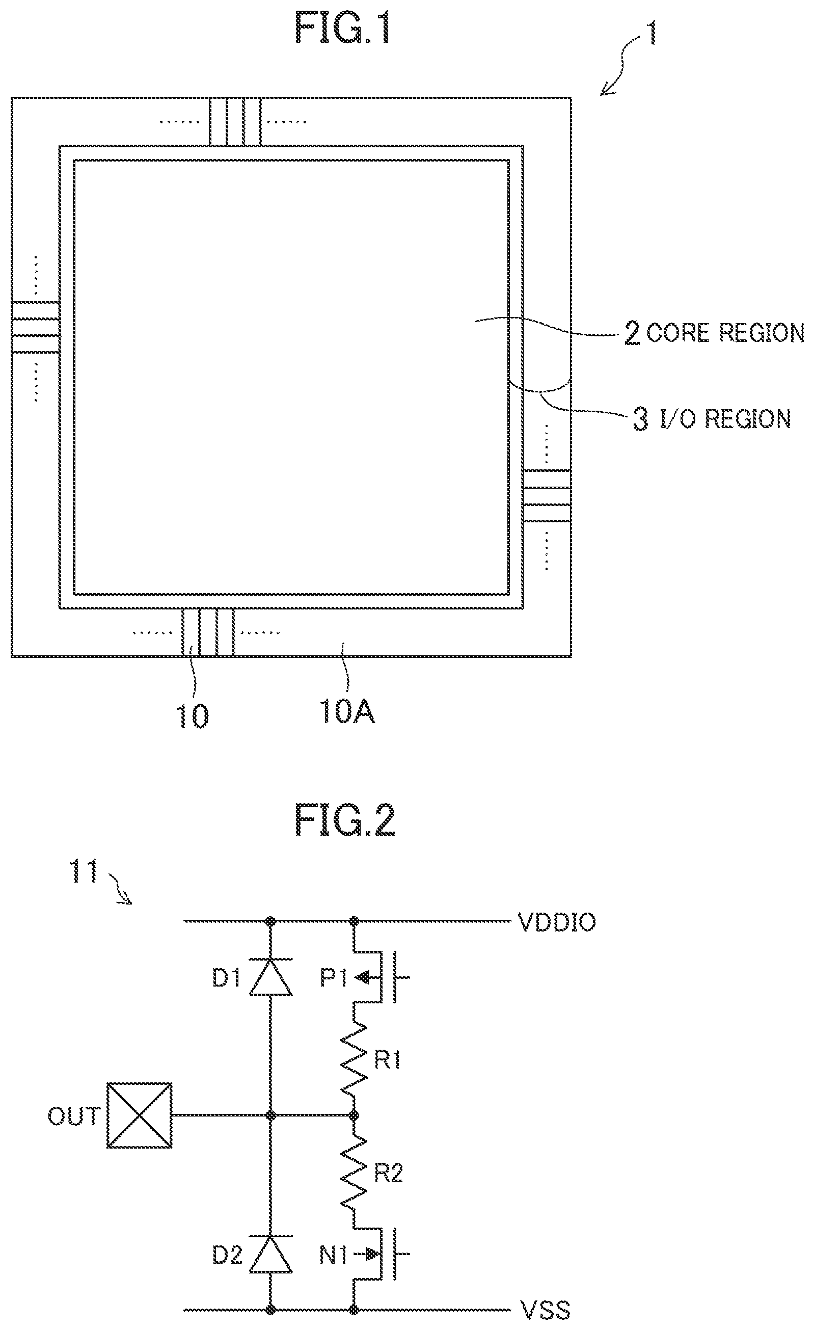
is a plan view schematically showing the entire configuration of a semiconductor integrated circuit device according to an embodiment. A semiconductor integrated circuit device 1 shown in includes a core region 2 in which inner core circuits are formed and an IO region 3 , provided around the core region 2 , in which interface circuits (IO circuits) are formed. In the IO region 3 , an IO cell row 10 A is provided to encircle the perimeter of the semiconductor integrated circuit device 1 . Although illustration is simplified in , a plurality of IO cells 10 constituting the interface circuits are arranged in the IO cell row 10 A. Also, although illustration is omitted, a plurality of external connection pads are placed in the semiconductor integrated circuit device 1 .
is a circuit diagram of an output circuit 11 included in the I/O cell 10 . Note that the actual output circuit also includes circuit elements other than those shown in although illustration of such elements is omitted.
The output circuit 11 shown in includes an external output terminal OUT, output transistors P 1 and N 1 , electrostatic discharge (ESD) protection diodes D 1 and D 2 , and protection resistances R 1 and R 2 . The output transistor Pb is a p-type transistor, and the output transistor N 1 is an n-type transistor.
The output transistors P 1 and N 1 output an output signal to the external output terminal OUT in accordance with signals received at their gates. The output transistor P 1 is connected to VDDIO at its source and to the external output terminal OUT through the protection resistance R 1 at its drain. The output transistor N 1 is connected to VSS at its source and to the external output terminal OUT through the protection resistance R 2 at its drain. The protection resistances R 1 and R 2 are constituted by a wiring resistance, for example, and such wiring is implemented by interconnects formed in a diffusion layer, a gate interconnect layer, or a metal interconnect layer, or a combination thereof.
The ESD protection diode D 1 is provided between VDDIO and the external output terminal OUT, and the ESD protection diode D 2 is provided between VSS and the external output terminal OUT. When high-voltage noise is input into the external output terminal OUT, current flows to VDDIO and VSS through the ESD protection diodes D 1 and D 2 , whereby the output transistors P 1 and N 1 are protected.
is a schematic view showing an example of the planar layout structure of the output circuit 11 according to this embodiment, in which the X direction (horizontal direction in the figure) is a direction along which the I/O cells 10 are arranged, and the Y direction (vertical direction in the figure) is a direction from the core region 2 side to the tip end side. The upper side in the figure is the core region 2 side, and the lower side in the figure is the tip end side. Regions in corresponding to the circuit elements in the circuit diagram of are denoted by the same reference characters.
The ESD protection diodes D 1 and D 2 are placed in the center in the Y direction. The output transistor P 1 is placed above the ESD protection diode D 1 in the figure in a location apart from the ESD protection diode D 1 . The output transistor N 1 is placed below the ESD protection diode D 2 in the figure in a location apart from the ESD protection diode D 2 .
The protection resistance R 1 is placed between the output transistor P 1 and the ESD protection diode D 1 , and formed as a plurality of separate regions (resistance regions) 21 . In the example of , the protection resistance R 1 is divided into four resistance regions 21 , each in a rectangular shape extending in the Y direction, arranged in the X direction. Tap regions 23 in which taps supplying VSS to the P-substrate are formed are placed to sandwich the resistance regions 21 .
The protection resistance R 2 is placed between the output transistor N 1 and the ESD protection diode D 2 , and formed as a plurality of separate regions (resistance regions) 22 . In the example of , the protection resistance R 2 is divided into four resistance regions 22 , each in a rectangular shape extending in the Y direction, arranged in the X direction. Tap regions 24 in which taps supplying VDDIO to the N-well are formed are placed to sandwich the resistance regions 22 .
Pads not shown are provided in a layer above the ESD protection diodes D 1 and D 2 , for connection with the outside of the semiconductor integrated circuit device.
The layout structures of the individual circuit elements will be described hereinafter in detail.
(Layout Structure of ESD Protection Diode)
shows a layout structure example of the ESD protection diode D 2 . Note that illustration of interconnect layers, etc. is omitted in .
As shown in , the ESD protection diode D 2 is formed in the P-substrate region in the center. The ESD protection diode D 2 includes an anode portion 31 formed of p-type fins 32 and cathode portions 33 a and 33 b formed of n-type fins 34 a and 34 b , respectively. The fins 32 , 34 a , and 34 b extend in the X direction. The anode portion 31 is connected to VSS, and the cathode portions 33 a and 33 b are connected to the external output terminal OUT. A diode is formed between the p-type fins 32 and the n-type fins 34 a and 34 b.
A guard ring 81 is formed around the ESD protection diode D 2 . The guard ring 81 includes n-type fins 82 formed on the N-well. The fins 82 extend in the X direction, and is connected to VDDIO.
Dummy gates 41 are formed for the fins 32 of the anode portion 31 and the fins 34 a and 34 b of the cathode portions 33 a and 33 b . Dummy gates 42 are formed for the fins 82 of the guard ring 81 . The dummy gates 41 and 42 extend in the Y direction. The formation of the dummy gates 41 and 42 improves the uniformity of the gate pattern in the semiconductor integrated circuit device, thereby improving the reliability and yield of the semiconductor integrated circuit device.
Note that the placement of the dummy gates 41 and 42 may be omitted. Also, the formation of the guard ring 81 may be omitted.
shows a layout structure example of the ESD protection diode D 1 . Note that illustration of interconnect layers, etc. is omitted in .
As shown in , the ESD protection diode D 1 is formed on the N-well in the center. The ESD protection diode D 1 includes a cathode portion 36 formed of n-type fins 37 and anode portions 38 a and 38 b formed of p-type fins 39 a and 39 b , respectively. The fins 37 , 39 a , and 39 b extend in the X direction. The cathode portion 36 is connected to VDDIO, and the anode portions 38 a and 38 b are connected to the external output terminal OUT. A diode is formed between the n-type fins 37 and the p-type fins 39 a and 39 b.
A guard ring 83 is formed around the ESD protection diode D 1 . The guard ring 83 includes p-type fins 84 formed in the P-substrate region. The fins 84 extend in the X direction, and is connected to VS S.
Dummy gates 43 are formed for the fins 37 of the cathode portion 36 and the fins 39 a and 39 b of the anode portions 38 a and 38 b . Dummy gates 44 are formed for the fins 84 of the guard ring 83 . The dummy gates 43 and 44 extend in the Y direction. The formation of the dummy gates 43 and 44 improves the uniformity of the gate pattern in the semiconductor integrated circuit device, thereby improving the reliability and yield of the semiconductor integrated circuit device.
Note that the placement of the dummy gates 43 and 44 may be omitted. Also, the formation of the guard ring 83 may be omitted.
(Layout Structure of Protection Resistance)
shows a layout structure example of the protection resistance R 2 . Note that illustration of interconnect layers, etc. is omitted in .
As shown in , and as described with reference to , the protection resistance R 2 is divided into four resistance regions 22 arranged in the X direction. A gate interconnect 51 is formed in each of the resistance regions 22 , and such gate interconnects 51 are mutually connected through an interconnect not shown, to form one resistance or a plurality of resistances. The gate interconnects 51 are formed on the N-well.
The tap regions 24 are placed to sandwich the resistance regions 22 . In the tap regions 24 , n-type fins 52 are formed on the N-well, serving as taps. The fins 52 extend in the X direction, and is connected to VDDIO. Dummy gates 45 extending in the Y direction are formed for the fins 52 .
While the gate interconnects 51 constituting the protection resistance are formed on the N-well, they may be formed on the P-substrate. Also, the taps in the tap regions 24 may be p-type fins formed on the P-substrate and connected to VSS.
shows a layout structure example of the protection resistance R 1 . Note that illustration of interconnect layers, etc. is omitted in .
As shown in , and as described with reference to , the protection resistance R 1 is divided into four resistance regions 21 arranged in the X direction. A gate interconnect 53 is formed in each of the resistance regions 21 , and such gate interconnects 53 are mutually connected through an interconnect not shown, to form one resistance or a plurality of resistances. The gate interconnects 53 are formed on the N-well.
The tap regions 23 are placed to sandwich the resistance regions 21 . In the tap regions 23 , p-type fins 54 are formed on the P-substrate, serving as taps. The fins 54 extend in the X direction, and is connected to VSS. Dummy gates 46 extending in the Y direction are formed for the fins 54 .
While the gate interconnects 53 constituting the protection resistance are formed on the N-well, they may be formed on the P-substrate. Also, the taps in the tap regions 23 may be n-type fins formed on the N-well and connected to VDDIO.
While the protection resistance is constituted by gate interconnects in this example, the configuration is not limited to this. It may be constituted by fins, metal interconnects, etc. Otherwise, the resistance may be constituted by a combination of gate interconnects, fins, metal interconnects, etc.
Note that the placement of the dummy gates 45 and 47 may be omitted.
While the taps are assumed to have fin-structure diffusion regions in this example, the configuration is not limited to this.
(Layout Structure of Output Transistor)
shows a layout structure example of the output transistor N 1 . Note that illustration of interconnect layers, etc. is omitted in .
As shown in , in the region of the output transistor N 1 in the center, formed are a plurality of n-type fins 61 , each extending in the X direction, arranged in the Y direction, and a plurality of gate interconnects 62 , each extending in the Y direction, arranged in the X direction. Portions where the fins 61 and the gate interconnects 62 overlap each other as viewed in plan form transistors. Such transistors are connected in parallel through interconnects not shown. The drains of the transistors are connected to the external output terminal OUT through the protection resistance R 2 .
A guard ring 85 is formed around the output transistor N 1 . The guard ring 85 includes p-type fins 86 formed on the P-substrate. The fins 86 extend in the X direction, and is connected to VSS. Dummy gates 47 are formed for the fins 86 .
Note that the placement of the dummy gates 47 may be omitted. Also, the formation of the guard ring 85 may be omitted.
shows a layout structure example of the output transistor P 1 . Note that illustration of interconnect layers, etc. is omitted in .
As shown in , in the region of the output transistor P 1 in the center, formed are a plurality of p-type fins 66 , each extending in the X direction, arranged in the Y direction, and a plurality of gate interconnects 67 , each extending in the Y direction, arranged in the X direction. Portions where the fins 66 and the gate interconnects 67 overlap each other as viewed in plan form transistors. Such transistors are connected in parallel through interconnects not shown. The drains of the transistors are connected to the external output terminal OUT through the protection resistance R 1 .
A guard ring 87 is formed around the output transistor P 1 . The guard ring 87 includes n-type fins 88 formed on the N-well. The fins 88 extend in the X direction, and is connected to VDDIO. Dummy gates 48 are formed for the fins 88 .
Note that the placement of the dummy gates 48 may be omitted. Also, the formation of the guard ring 87 may be omitted.
According to this embodiment, the output transistor P 1 is placed apart from the ESD protection diode D 1 connected to the external output terminal OUT, with the protection resistance R 1 interposed between them. The output transistor N 1 is placed apart from the ESD protection diode D 2 connected to the external output terminal OUT, with the protection resistance R 2 interposed between them. With this configuration, noise applied to the external output terminal OUT is attenuated by the protection resistances R 1 and R 2 before reaching the output transistors P 1 and N 1 . Also, the protection resistance R 1 is formed as a plurality of separate resistance regions 21 , and taps supplying VSS to the P-substrate are formed in the tap regions 23 provided between the resistance regions 21 . The protection resistance R 2 is formed as a plurality of separate resistance regions 22 , and taps supplying VDDIO to the N-well are formed in the tap regions 24 provided between the resistance regions 22 . With this configuration, noise applied to the external output terminal OUT is absorbed through the taps. It is therefore possible to control propagation of noise that is to be a cause of occurrence of the latch-up phenomenon. In addition, with the tap regions 23 and 24 being dispersed in a plurality of places, the effect of absorbing noise can be obtained more uniformly.
Referring to , control of the occurrence of the latch-up phenomenon will be described. is a schematic cross-sectional view of the semiconductor integrated circuit device of this embodiment, in which the ESD protection diode D 2 , the protection resistance R 2 +well tap portion (illustration of the protection resistance R 2 is omitted), the output transistor N 1 , and other transistors are arranged sequentially from right to left.
Assume here that noise is applied to the external output terminal OUT (A in ). If the noise propagates up to the output transistor N 1 and other transistors without being sufficiently reduced, a current will flow to the base of a parasitic bipolar transistor due to the noise having propagated. This will cause a latch-up phenomenon via the parasitic transistor, resulting in occurrence of a large current between VDDIO and VSS (B in ).
According to the configuration of this embodiment, however, noise is attenuated since the protection resistance R 2 is interposed between the ESD protection diode D 2 and the output transistor N 1 , separating the diode D 2 from other transistors. Also, noise (A in ) at the external output terminal OUT is absorbed through routes indicated by D in via the taps provided in the region of the protection resistance R 2 , whereby fluctuations of the potential at the base node (C in ) of the parasitic bipolar transistor can be controlled. It is therefore possible to suppress noise that may propagate up to the output transistor N 1 and other transistors, and thus control the occurrence of the latch-up phenomenon.
(Alteration)
is a schematic view showing another example of the planar layout structure of the output circuit 11 . In the example of , the protection resistance R 1 is divided into four resistance regions 21 A, each in a rectangular shape extending in the X direction, arranged in the Y direction. Tap regions 23 A in which taps supplying VSS to the P-substrate are formed are placed to sandwich the resistance regions 21 A.
The protection resistance R 2 is divided into four resistance regions 22 A, each in a rectangular shape extending in the X direction, arranged in the Y direction. Tap regions 24 A in which taps supplying VDDIO to the N-well are formed are placed to sandwich the resistance regions 22 A.
In this alteration, also, similar effects to those in the above embodiment are obtained. That is, noise applied to the external output terminal OUT is attenuated by the protection resistances R 1 and R 2 before reaching the output transistors P 1 and N 1 . Also, noise applied to the external output terminal OUT is absorbed through the taps formed in the tap regions 23 A and 24 A. It is therefore possible to control propagation of noise that is to be a cause of occurrence of the latch-up phenomenon. In addition, with the tap regions 23 A and 24 A being dispersed in a plurality of places, the effect of absorbing noise can be obtained more uniformly.
While the protection resistances R 1 and R 2 are divided in the X direction in and divided in the Y direction in , the division may be made in a mixed manner. For example, a layout in which the protection resistance R 1 is divided in the X direction and the protection resistance R 2 in the Y direction may be used.
Second Embodiment
is a circuit diagram of an output circuit 12 according to this embodiment. The configuration of is roughly the same as the circuit configuration of , except for the position of insertion of a protection resistance. That is, the output circuit 12 of includes a protection resistance R 3 in place of the protection resistances R 1 and R 2 in . In , the drains of the output transistors P 1 and N 1 are mutually connected, and the protection resistance R 3 is provided between the external output terminal OUT and the drains of the output transistors P 1 and N 1 .
is a schematic view showing an example of the planar layout structure of the output circuit 12 according to this embodiment, in which the X direction (horizontal direction in the figure) is a direction along which I/O cells 10 are arranged, and the Y direction (vertical direction in the figure) is a direction from the core region 2 side to the tip end side. The upper side in the figure is the core region 2 side, and the lower side in the figure is the tip end side. Regions in corresponding to the circuit elements in the circuit diagram of are denoted by the same reference characters. Pads not shown are provided in a layer above the ESD protection diodes D 1 and D 2 , for connection with the outside of the semiconductor integrated circuit device.
The ESD protection diodes D 1 and D 2 are placed adjacent to each other in the Y direction, and the output transistors P 1 and N 1 are placed adjacent to each other in the Y direction. The ESD protection diodes D 1 and D 2 lie in a lower part in the figure, and the output transistors P 1 and N 1 lie above the ESD protection diodes D 1 and D 2 in the figure in a location apart from the ESD protection diodes D 1 and D 2 .
The protection resistance R 3 is placed between the output transistors P 1 and N 1 and the ESD protection diodes D 1 and D 2 , and formed as a plurality of separate regions (resistance regions) 121 . In the example of , the protection resistance R 3 is divided into four resistance regions 121 , each in a rectangular shape extending in the Y direction, arranged in the X direction. Tap regions 122 in which taps supplying VSS to the P-substrate are formed and tap regions 123 in which taps supplying VDDIO to the N-well are formed are placed between the resistance regions 121 . In the example of , the tap regions 122 and the tap regions 123 are placed alternately in the Y direction. That is, in a single region between the adjacent resistance regions 121 , formed are the taps supplying VSS to the P-substrate and the taps supplying VDDIO to the N-well.
According to this embodiment, the output transistors P 1 and N 1 are placed apart from the ESD protection diodes D 1 and D 2 connected to the external output terminal OUT, with the protection resistance R 3 interposed between them. With this configuration, noise applied to the external output terminal OUT is attenuated by the protection resistance R 3 before reaching the output transistors P 1 and N 1 . Also, the protection resistance R 3 is formed as a plurality of separate resistance regions 121 . Taps supplying VSS to the P-substrate are formed in the tap regions 122 between the resistance regions 121 , and taps supplying VDDIO to the N-well are formed in the tap regions 123 between the resistance regions 121 . With this configuration, noise applied to the external output terminal OUT is absorbed through the taps. It is therefore possible to control propagation of noise that is to be a cause of occurrence of the latch-up phenomenon. In addition, with the tap regions 122 and 123 being dispersed in a plurality of places, the effect of absorbing noise can be obtained more uniformly.
The tap regions 122 including taps supplying VSS to the P-substrate work for absorbing noise from the ESD protection diode D 1 , and the tap regions 123 including taps supplying VDDIO to the N-well work for absorbing noise from the ESD protection diode D 2 .
Note that the positions of the ESD protection diodes D 1 and D 2 may be changed with each other, and the positions of the output transistors P 1 and N 1 may be changed with each other.
(Alterations)
A and 14 B are schematic views showing other examples of the planar layout structure of the output circuit 12 . In the example of A , tap regions 122 A in which taps supplying VSS to the P-substrate are formed and tap regions 123 A in which taps supplying VDDIO to the N-well are formed are placed alternately in the X direction between the resistance regions 121 .
In the example of B , the protection resistance R 3 is divided into four resistance regions 121 A, each in a rectangular shape extending in the X direction, arranged in the Y direction. Tap regions 122 B in which taps supplying VSS to the P-substrate are formed and tap regions 123 B in which taps supplying VDDIO to the N-well are formed are placed between the resistance regions 121 A. In the example of B , the tap regions 122 B and the tap regions 123 B are placed alternately in the X direction.
Note that, in the example of B , the tap regions 122 B and the tap regions 123 B may be placed alternately in the Y direction.
In these alterations, also, similar effects to those in the above embodiment are obtained. That is, noise applied to the external output terminal OUT is attenuated by the protection resistance R 3 before reaching the output transistors P 1 and N 1 . Also, noise applied to the external output terminal OUT is absorbed through the taps formed in the tap regions 122 A and 123 A or the tap regions 122 B and 123 B. It is therefore possible to control propagation of noise that is to be a cause of occurrence of the latch-up phenomenon. In addition, with the tap regions 122 A and 123 A or the tap regions 122 B and 123 B being dispersed in a plurality of places, the effect of absorbing noise can be obtained more uniformly.
In the above embodiments, while the protection resistances R 1 , R 2 , and R 3 are each divided into four resistance regions, the number of resistance regions is not limited to four.
In the output circuits in the above embodiments, while the p-type output transistor and the n-type output transistor are both one-stage transistors, the transistor configuration is not limited to this. For example, the transistors may be transistors of a plurality of stages, such as two-stage transistors and three-stage transistors, connected in series. Also, the output circuits in each of the above embodiments may be an input/output circuit including an input circuit.
According to the present disclosure, the occurrence of the latch-up phenomenon can be sufficiently controlled. The present disclosure is therefore useful for improvement of the performance of semiconductor chips, for example.
Figures (13)
Citations
This patent cites (31)
- US8228651
- US20050179088
- US20070201175
- US20070258176
- US20070279824
- US20100155845
- US20110026176
- US20130264647
- US20140198416
- US20140376135
- US20150043116
- US20160094027
- US20170323879
- US20180197850
- US20180205225
- US20200203334
- US20210111173
- US20210288145
- US20210408786
- US20220262787
- US20220376495
- US107112281
- US112670283
- US115241855
- US1289016
- US2010-147282
- US2011-096897
- US2014-064044
- US2016-072349
- US2022163499
- US2019/043888