Abstract
According to one embodiment, a semiconductor memory device includes a plurality of first interconnect layers, first and second memory pillars, and a plurality of first plugs. The plurality of first interconnect layers include a first array region where the first memory pillar penetrates the plurality of first interconnect layers, a second array region where the second memory pillar penetrates the plurality of first interconnect layers, and a coupling region where a plurality of coupling parts respectively coupled to the plurality of first plugs are formed. Along a first direction parallel to the semiconductor substrate, the first array region, the coupling region, and the second array region are arranged in order.
Claims (12)
1. A semiconductor memory device comprising: a plurality of first conductive layers stacked in a first direction and disposed between nearest of two first slits in a second direction; a second conductive layer disposed above the plurality of first conductive layers and disposed between one of the nearest two first slits and a second slit; a third conductive layer disposed above the plurality of first conductive layers and disposed between another of the nearest two first slits and the second slit; a first pillar extending through the plurality of first conductive layers and the second conductive layer in the first direction, the first pillar including a semiconductor layer; a second pillar extending through the plurality of first conductive layers and the third conductive layer in the first direction, the second pillar including a semiconductor layer; a first plug extending in the first direction and in contact with the second conductive layer; a second plug extending in the first direction and in contact with the third conductive layer; a third plug extending through the plurality of first conductive layers and the second conductive layer in the first direction and electrically connected to the first plug; and a fourth plug extending through the plurality of first conductive layers and the third conductive layer in the first direction and electrically connected to the second plug.
Show 11 dependent claims
2. The device according to claim 1 , further comprising: a first insulating layer provided between the third plug and the plurality of first conductive layers; and a second insulating layer provided between the fourth plug and the plurality of first conductive layers, wherein the third plug and the fourth plug are not in contact with the plurality of first conductive layers.
3. The device according to claim 1 , further comprising: a fifth plug extending in the first direction and in contact with a first layer among the plurality of first conductive layers; and a sixth plug extending in the first direction and in contact with a second layer among the plurality of first conductive layers, wherein the first layer and the second layer are arranged stepwise along a third direction crossing the first direction and the second direction.
4. The device according to claim 3 , wherein the first layer and the second layer are arranged in a two-stage stepwise shape.
5. The device according to claim 1 , wherein the first and second pillars each include a third insulating layer, a charge storage layer, and a fourth insulating layer, which are provided in order on a side surface of the semiconductor layer.
6. The device according to claim 1 , further comprising a circuit provided below the plurality of first conductive layers and to which bottom surfaces of the third and fourth plugs are electrically coupled.
7. The device according to claim 6 , wherein the circuit is a row decoder.
8. The device according to claim 1 , further comprising a fourth conductive layer provided above the first and second pillars and electrically coupled to the semiconductor layer of the first pillar and the semiconductor layer of the second pillar.
9. The device according to claim 8 , further comprising a sense amplifier to which the fourth conductive layer is electrically coupled.
10. The device according to claim 1 , further comprising a fifth conductive layer provided below the plurality of first conductive layers and contacting bottom surfaces of the first and second pillars.
11. The device according to claim 1 , wherein end portions of the plurality of first conductive layers are arranged stepwise along a third direction crossing the first direction and the second direction.
12. The device according to claim 1 , further comprising: a sixth conductive layer disposed above the plurality of first conductive layers and disposed in a third direction crossing the first direction and the second direction of the second conductive layer; a seventh conductive layer disposed above the plurality of first conductive layers, disposed in the third direction of the third conductive layer, and disposed in the second direction of the sixth conductive layer; a third pillar extending through the plurality of first conductive layers and the sixth conductive layer, the third pillar including a semiconductor layer; and a fourth pillar extending through the plurality of first conductive layers and the seventh conductive layer, the fourth pillar including a semiconductor layer, wherein the first and third plugs are disposed between the first pillar and the third pillar, and the second and fourth plugs are disposed between the second pillar and the fourth pillar.
Full Description
Show full text →
CROSS-REFERENCE TO RELATED APPLICATIONS
This application is a continuation of U.S. application Ser. No. 17/087,724 filed Nov. 3, 2020, which is a continuation of U.S. application Ser. No. 16/751,293 filed Jan. 24, 2020 which is a continuation of U.S. application Ser. No. 16/118,598 filed Aug. 31, 2018, and is based upon and claims the benefit of priority from Japanese Patent Application No. 2018-046940, filed Mar. 14, 2018, the entire contents of each of which are incorporated herein by reference.
FIELD
Embodiments described herein relate generally to a semiconductor memory device.
BACKGROUND
A NAND flash memory is known as a semiconductor memory device.
BRIEF DESCRIPTION OF THE DRAWINGS
is a block diagram of a semiconductor memory device according to a first embodiment;
is a circuit diagram of a memory cell array in the semiconductor memory device according to the first embodiment;
is a plan view of the memory cell array in the semiconductor memory device according to the first embodiment;
is a cross-sectional view taken along a line A 1 -A 2 in ;
is a cross-sectional view taken along a line B 1 -B 2 in ;
is a cross-sectional view taken along a line C 1 -C 2 in ;
are diagrams illustrating a manufacturing process of a step part of the memory cell array in the semiconductor memory device according to the first embodiment;
is a cross-sectional view of a memory cell array of a comparative example, and the memory cell array in the semiconductor memory device according to the first embodiment;
is a plan view of a memory cell array in a semiconductor memory device according to a second embodiment; and
are diagrams illustrating a manufacturing process of a step part of the memory cell array in the semiconductor memory device according to the second embodiment.
DETAILED DESCRIPTION
In general, according to one embodiment, a semiconductor memory device includes: a plurality of first interconnect layers stacked above a semiconductor substrate with first insulating layers interposed therebetween, first and second memory pillars penetrating the plurality of first interconnect layers, and a plurality of first plugs, bottom surfaces of which are in respective contact with the plurality of first interconnect layers. The plurality of first interconnect layers include a first array region where the first memory pillar penetrates the plurality of first interconnect layers, a second array region where the second memory pillar penetrates the plurality of first interconnect layers, and a coupling region where a plurality of coupling parts respectively coupled to the plurality of first plugs are formed. The first array region, the coupling region, and the second array region are arranged in order along a first direction parallel to the semiconductor substrate.
1. First Embodiment
Here, a semiconductor memory device according to a first embodiment will be described. In the following descriptions, as a semiconductor memory device, a three-dimensional stacked NAND flash memory in which memory cell transistors are stacked three-dimensionally on the semiconductor substrate will be described by way of example.
1.1 Configuration
1.1.1 General Configuration of the Semiconductor Memory Device
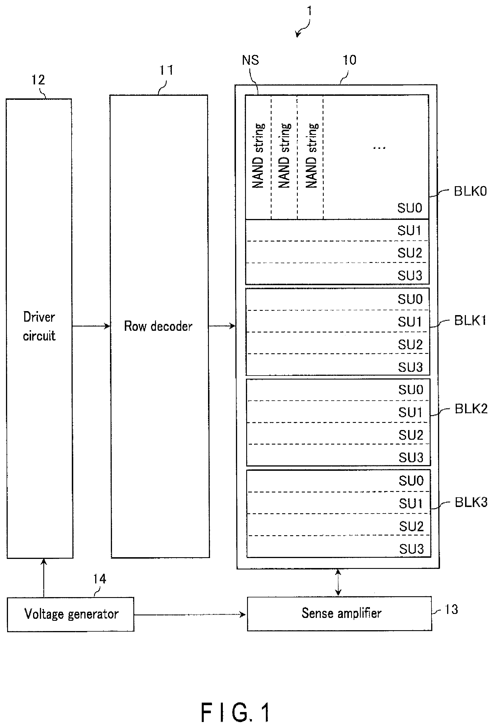
First, a general configuration of a semiconductor memory device will be described using . is an example of a block diagram illustrating a basic general configuration of a semiconductor memory device. In the example of , a part of the coupling of each block is indicated by an arrow line. However, coupling between the blocks is not limited to this.
As shown in , a NAND flash memory 1 includes a memory cell array 10 , a row decoder 11 , a driver circuit 12 , a sense amplifier 13 , and a voltage generator 14 .
The memory cell array 10 includes a plurality (in the present embodiment, four) of blocks BLK (BLK 0 to BLK 3 ) which are aggregates of non-volatile memory cell transistors. Each of the blocks BLK includes a plurality (in the present embodiment, four) of string units SU (SU 0 to SU 3 ) that are an aggregate of NAND strings NS in which the memory cell transistors are coupled in series. The number of blocks BLK in the memory cell array 10 and the number of string units SU in the block BLK are discretionary.
The row decoder 11 includes a block decoder and a hookup circuit which are not depicted in the drawings. The block decoder decodes a row address, and selects a row direction of a corresponding block BLK based on the decoding result. The row decoder 11 is coupled to word lines and select gate lines of each block BLK via the hookup circuit.
The driver circuit 12 supplies voltage necessary for a write operation, a read operation, and an erase operation of data to the row decoder 11 . This voltage is applied to corresponding word lines and select gate lines via the row decoder 11 .
The sense amplifier 13 senses data which has been read from the memory cell transistor during a data read operation. In addition, during a data write operation, the written data is transferred to the memory cell transistor.
The voltage generator 14 generates voltage necessary for the data write, read, and erase operations, and supplies it to the driver circuit 12 , the sense amplifier 13 , etc.
1.1.2 Configuration of the Memory Cell Array
Next, a configuration of the memory cell array 10 will be described using . An example of illustrates a block BLK 0 , however the other blocks BLK also have the same configuration.
As shown in , the block BLK 0 includes, for example, four string units, SU 0 to SU 3 . Each string unit SU includes a plurality of NAND strings NS. Each of the NAND strings NS includes, for example, eight memory cell transistors MT (MT 0 to MT 7 ) and select transistors ST 1 and ST 2 . The memory cell transistor MT comprises a control gate and a charge storage layer, and stores data in a nonvolatile manner.
It should be noted that the memory cell transistors MT may be of a MONOS type in which an insulating film is used as the charge storage layer, or an FG type in which a conductive film is used as the charge storage layer. In the present embodiment, a MONOS type will be explained by way of example. In addition, the number of the memory cell transistors MT is not limited to 8, and may be, for example, 16, 32, 64, 96, and 128. The number of the memory cell transistors MT is not limited. Moreover, the number of the select transistors ST 1 and ST 2 is discretionary, and each may be a number greater than one.
The eight memory cell transistors MT are coupled in series between a source of the select transistor ST 1 and a drain of the select transistor ST 2 . More specifically, current paths of the memory cell transistors MT 0 to MT 7 are coupled in series. Subsequently, a drain of the memory cell transistor MT 7 is coupled to a source of the select transistor ST 1 , and a source of the memory cell transistor MT 0 is coupled to a drain of the select transistor ST 2 .
A gate of the select transistor ST 1 in each of the string units SU 0 to SU 3 is coupled to different select gate lines SGD 0 to SGD 3 , respectively, for every string unit SU. A more specific example might see gates of a plurality of select transistors ST 1 in the string SU 0 commonly coupled to a select gate line SGD 0 .
The gates of the select transistors ST 2 in the string units SU 0 to SU 3 are commonly coupled to the select gate line SGS. Namely, the gates of a plurality of select transistors ST 2 in the same block BLK are commonly coupled to the select gate line SGS. It should be noted that a gate of the select transistor ST 2 in each of the string units SU 0 to SU 3 may be coupled to different select gate lines SGS 0 to SGS 3 , respectively, for every string unit SU.
Control gates of the memory cell transistors MT 0 to MT 7 in the same block BLK are commonly coupled to the word lines WL 0 to WL 7 , respectively. More specifically, for example, control gates of a plurality of memory cell transistors MT 0 in the block BLK 0 are commonly coupled to a word line WL 0 .
Drains of a plurality of select transistors ST 1 in a string unit SU are respectively coupled to different bit lines BL (BL 0 to BL(n−1), where “n” is a natural number of 2 or more). Namely, a plurality of NAND strings NS in a string unit SU are respectively coupled to different bit lines BL. In addition, a bit line BL commonly couples one NAND string NS included in each of the string units SU 0 to SU 3 in each block BLK.
Sources of the select transistors ST 2 in a plurality of blocks BLK are commonly coupled to a source line SL.
Namely, a string unit SU is an aggregate of the NAND strings NS, each of which is coupled to a different bit line BL and is coupled to the same select gate line SGD. In addition, a block BLK is an aggregate of a plurality of string units SU sharing the word lines WL. The memory cell array 10 is an aggregate of a plurality of blocks BLK which share the bit lines BL.
It should be noted that the memory cell array 10 may be configured in a different manner. That is, the configuration of the memory cell array 10 is described, for example, in U.S. patent application Ser. No. 12/407,403 entitled “THREE DIMENSIONAL STACKED NONVOLATILE SEMICONDUCTOR MEMORY” filed on Mar. 19, 2009. The configuration of the memory cell array 10 is also described in U.S. patent application Ser. No. 12/406,524 entitled “THREE DIMENSIONAL STACKED NONVOLATILE SEMICONDUCTOR MEMORY” filed on Mar. 18, 2009; U.S. patent application Ser. No. 12/679,991 entitled “NON-VOLATILE SEMICONDUCTOR STORAGE DEVICE AND METHOD OF MANUFACTURING THE SAME” filed on Mar. 25, 2010; and U.S. patent application Ser. No. 12/532,030 entitled “SEMICONDUCTOR MEMORY AND METHOD FOR MANUFACTURING SAME” filed on Mar. 23, 2009. The entire contents of these applications are incorporated herein by reference.
1.1.3 Plane Configuration of the Memory Cell Array
Next, a plane configuration of the memory cell array 10 will be described using . is a plan view of string units SU 0 to SU 4 in one block BLK. It should be noted that in an example of , an inter-layer insulating film is omitted.
As shown in , in the memory cell array 10 in the present embodiment, the word lines WL and the select gate line SGS are shared in the string units SU 0 and SU 1 . Subsequently, a slit SHE is formed between the select gate line SGD 0 of the string unit SU 0 and the select gate line SGD 1 of the string unit SU 1 so that the select gate lines SGD 0 and SGD 1 are separated. The same applies to the string units SU 2 and SU 3 . A slit SLT is formed between the string units SU 1 and SU 2 so that respective select gate lines SGD and SGS and word lines WL are separated.
The memory cell array 10 comprises two array parts, a step part, and two dummy step parts. More specifically, along a first direction D 1 parallel to the semiconductor substrate, from one end of the memory cell array 10 to the other, the dummy step part, the array part, the step part, the array part, and the dummy step part are arranged in order, and the step part is arranged in the center of the memory cell array 10 . Namely, the word line WL has regions corresponding to two array parts, a step part, and two dummy step parts along the first direction D 1 , and the step part is provided between the two array parts.
In the array part, a memory pillar MP corresponding to a NAND string NS is formed. Details of a configuration of the memory pillar MP will be described later. In the example of , in each string unit SU, a plurality of memory pillars MP are arranged in a row along the first direction D 1 . For example, an upper end of the memory pillar MP of each string unit SU, arranged along a second direction parallel to the semiconductor substrate and at a right angle to the first direction D 1 , is commonly coupled by a bit line BL.
The select gate lines SGD 0 to SGD 3 corresponding to the two array parts are respectively separated in the step part. Thus, in one string unit SU, either one of the two array parts is chosen by selecting either one of the separated select gate lines SGD.
It should be noted that an arrangement of the memory pillars MP in one string unit SU can be discretionarily set. For example, along the first direction D 1 , the memory pillars MP may be arranged in two parallel rows, or in a four-line staggered layout.
In the step part, a plurality of interconnect layers corresponding to the select gate lines SGD and SGS and the word lines WL 0 to WL 7 are led stepwise (hereinafter, a lead-out portion will be referred to as “terrace.”). Namely, terraces of the word lines WL 0 to WL 7 are formed in the center of the interconnect layers corresponding to the word lines WL 0 to WL 7 in the first direction D 1 . A contact plug CC is formed on each terrace. In the step part, to couple the row decoder 11 (a hookup circuit) formed in a lower layer of the memory cell array 10 to the contact plugs CC, contact plugs C 4 which penetrate the memory cell array 10 are formed. Upper ends of the contact plugs CC and contact plugs C 4 are coupled by an interconnect layer. The contact plugs CC and C 4 are made from conductive materials. For example, metal materials, such as tungsten (W) and nitride titanium (TiN), etc., may be used. An insulating layer (e.g., a silicon oxide film-not depicted in the drawings) is formed on a side surface of the contact plug C 4 , and the contact plug C 4 is not electrically coupled to the select gate line SGS, the word lines WL 0 to WL 7 , and the select gate line SGD.
The select gate line SGD of each string unit SU is separated into two in the step part of the first direction D 1 , and the contact plugs CC and C 4 corresponding to each separated select gate line SGD are respectively arranged along the first direction D 1 .
In the step part of the string unit SU 0 , a terrace of the word line WL 7 is arranged between the two select gate lines SGD 0 . Subsequently, to penetrate this terrace, the contact plugs C 4 corresponding to the word lines WL 6 , WL 4 , WL 2 , and WL 0 , the select gate line SGS, and the word lines WL 1 , WL 3 , WL 5 , and WL 7 are arranged in order along the first direction D 1 .
In the step part of the string unit SU 1 , terraces of the word lines WL 6 , WL 4 , WL 2 , and WL 0 , the select gate line SGS, and the word lines WL 1 , WL 3 , WL 5 , and WL 7 are arranged in order along the first direction D 1 between the two select gate lines SGD 1 . Namely, the terraces of the word lines WL 0 to WL 7 corresponding to the string units SU 0 and SU 1 are arranged in a row along the first direction D 1 . Subsequently, a contact plug CC is arranged on each terrace. That is, the contact plugs CC corresponding to the word lines WL 6 , WL 4 , WL 2 , and WL 0 , the select gate line SGS, and the word lines WL 1 , WL 3 , WL 5 , and WL 7 are arranged in order along the first direction D 1 .
In the step parts of the string units SU 2 and SU 3 , terraces and contact plugs CC and C 4 are arranged so as to be symmetrical with the step parts of the string units SU 0 and SU 1 , with a slit SLT interposed therebetween.
More specifically, in the step part of the string unit SU 2 , the terraces of the word lines WL 6 , WL 4 , WL 2 , and WL 0 , the select gate line SGS, and the word lines WL 1 , WL 3 , WL 5 , and WL 7 are arranged in order along the first direction D 1 between the two select gate lines SGD 2 . Subsequently, a contact plug CC is arranged on each of the terraces.
In the step part of the string unit SU 3 , the terrace of the word line WL 7 is arranged between the two select gate lines SGD 3 . Subsequently, to penetrate this terrace, the contact plugs C 4 corresponding to the word lines WL 6 , WL 4 , WL 2 , and WL 0 , the select gate line SGS, and the word lines WL 1 , WL 3 , WL 5 , and WL 7 are arranged in order along the first direction D 1 .
It should be noted that the terraces and the contact plugs CC of the select gate line SGS and the word lines WL may be formed in the step part of the string unit SU 0 , and the contact plugs C 4 corresponding to the select gate line SGS and the word lines WL may be formed in the step part of the string unit SU 1 . The step parts of the string units SU 2 and SU 3 are configured in the same manner. Furthermore, the arrangement of the terraces in the first direction can be discretionarily set.
In addition, in the step part, a plurality of dummy pillars HR are provided, penetrating a plurality of interconnect layers corresponding to the select gate lines SGD and SGS and the word lines WL 0 to WL 7 . The arrangement of the dummy pillars is discretionary. The dummy pillars HR are not electrically coupled to the other interconnects as insulating layers are formed on the side and bottom surfaces of the dummy pillars. The dummy pillar HR functions as a pillar which, when filling air spaces corresponding to the select gate lines SGD and SGS and the word lines WL with, for example, a metal such as tungsten (W), supports an inter-layer insulating film between the select gate lines SGD and SGS and the word lines WL which have become those air spaces.
The dummy step parts are formed in a step-part-forming process. The width of the dummy step part in the first direction D 1 is narrower than that of the step part. In the dummy step part, the memory pillar MP, contact plugs CC and C 4 , etc. are not formed. It should be noted that the dummy step part may not be formed.
1.1.4 Cross-Sectional Configuration of the Memory Cell Array
Next, a cross-sectional configuration of the memory cell array 10 will be described using to 6 . is a cross-sectional view of the memory cell array 10 taken along a line A 1 -A 2 shown in . is a cross-sectional view of the memory cell array 10 taken along a line B 1 -B 2 shown in . is a cross-sectional view of the memory cell array 10 taken along a line C 1 -C 2 shown in . It should be noted that, to simplify the descriptions, in examples of , the circuits provided in a lower layer of the memory cell array 10 are depicted by blocks, and the interconnect layers on the memory pillars MP and the contact plugs CC and C 4 are omitted. In addition, in the example of , the circuits arranged below the memory cell array 10 are omitted.
As shown in , on a semiconductor substrate 100 , for example, circuits, such as the row decoder 11 and the sense amplifier 13 , are formed, and via the insulating layer 101 , the memory cell array 10 is formed above these circuits. As the insulating layer 101 , for example, a silicon oxide film (SiO 2 ) is used. It should be noted that the circuits arranged below the memory cell array 10 are not limited to the row decoder 11 and the sense amplifier 13 . More specifically, in a region of the memory cell array 10 , an interconnect layer 102 which functions as a source line SL is formed on the insulating layer 101 , and ten interconnect layers 103 which function as the select gate line SGS, the word lines WL 0 to WL 7 , and the select gate line SGD are further stacked thereon via the insulating layers 101 which lie between the interconnect layers. The interconnect layers 102 and 103 are made from conductive materials. For example, metal materials, such as W or TiN, may be used.
In the array parts of the memory cell array 10 , the memory pillars MP, which penetrate the ten interconnect layers 103 and bottom surfaces of which are in contact with the interconnect layer 102 , are formed.
In the step part of the string unit SU 1 , terraces of the select gate lines SGD and SGS and the word lines WL 0 to WL 7 are formed. More specifically, along the first direction D 1 , a terrace of the select gate line SGD 1 is formed; terraces of the even-numbered word lines WL 6 , WL 4 , WL 2 , and WL 0 are formed consecutively in a two-stage stepwise shape, a terrace of the select gate line SGS is formed; and terraces of the odd-numbered word lines WL 1 , WL 3 , WL 5 , and WL 7 are formed consecutively in a two-stage stepwise shape, and then a terrace of the select gate line SGD 1 is formed.
A contact plug CC is formed on each of the terraces. A contact plug C 4 corresponding to the select gate line SGD 1 is formed so as to penetrate the ten interconnect layers 103 and the interconnect layer 102 to be coupled to the row decoder 11 . In the example of , along the first direction D 1 , a contact plug C 4 corresponding to the select gate line SGD 1 , eleven contact plugs CC corresponding to the select gate line SGD 1 , the word lines WL 6 , WL 4 , WL 2 , and WL 0 , the select gate line SGS, the word lines WL 1 , WL 3 , WL 5 , and WL 7 , and the select gate line SGD 1 , and a contact plug C 4 corresponding to the select gate line SGD 1 are arranged in order.
As shown in , in the step part of the string unit SU 0 , the terraces of the select gate line SGD 0 and the word line WL 7 are formed. In the terrace of the word line WL 7 , the contact plugs C 4 corresponding to the select gate line SGS and word lines WL 0 to WL 7 are formed so as to penetrate nine interconnect layers 103 corresponding to the select gate line SGS and word lines WL 0 to WL 7 and the interconnect layer 102 , and to be coupled to the row decoder 11 . A contact plug CC is formed on the terrace of the select gate lines SGD 0 . In addition, a contact plug C 4 corresponding to the select gate line SGD 0 is formed to penetrate the ten interconnect layers 103 and interconnect layer 102 to be coupled to the row decoder 11 . In an example of , along the first direction D 1 , the contact plugs C 4 and CC corresponding to the select gate lines SGD 0 , nine contact plugs C 4 corresponding to the word lines WL 6 , WL 4 , WL 2 , and WL 0 , the select gate line SGS, and the word lines WL 1 , WL 3 , WL 5 , and WL 7 , and contact plugs CC and C 4 corresponding to the select gate lines SGD 0 are arranged in order.
Next, details of a cross-sectional configuration of the memory pillar MP will be described.
As shown in , the interconnect layer 102 that functions as a source line SL is common to the string units SU 0 to SU 3 . The slit SLT is formed between the string units SU 1 and SU 2 and extends along the first direction D 1 , also separating the ten interconnect layers 103 . It should be noted that the slit SLT is also formed between the blocks BLK (not depicted in the drawings). A slit SHE is formed between the string units SU 0 and SU 1 , and between the string units SU 2 and SU 3 . The slit SHE formed between the string units SU 0 and SU 1 separates the select gate lines SGD 0 and SGD 1 . The slit SHE formed between the string units SU 2 and SU 3 separates the select gate lines SGD 2 and SGD 3 .
On the semiconductor substrate 100 , the insulating layer 101 is formed via a circuit, such as a sense amplifier (not depicted in the drawings), etc., and the interconnect layer 102 that functions as a source line SL is formed thereon.
On the interconnect layer 102 , the ten interconnect layers 103 that function as, from the lower layer, the select gate line SGS, the word lines WL 0 to WL 7 , and the select gate line SGD are formed via the insulating layers 101 which lie between the interconnect layers.
The memory pillar MP includes a block insulating film 107 , a charge storage layer 106 , a tunnel insulating film 105 , and a semiconductor layer 104 . Then, by the memory pillar MP and the word lines WL 0 to WL 7 , memory cell transistors MT 0 to MT 7 are constituted. Similarly, by the memory pillar MP and the select gate lines SGD and SGS, the select transistors ST 1 and ST 2 are constituted.
More specifically, a memory hole is formed to penetrate the ten interconnect layers 103 and the insulating layers 101 to reach the interconnect layer 102 so as to form the memory pillar MP. On a side surface of the memory hole, the block insulating film 107 , the charge storage layer 106 , and the tunnel insulating film 105 are sequentially formed. An inner portion of the memory hole is filled with the semiconductor layer 104 . The semiconductor layer 104 constitutes a region where the memory cell transistor MT and channels of the select transistors ST 1 and ST 2 are formed. SiO 2 , for example, can be used as the block insulating film 107 and the tunnel insulating film 105 . SiN, for example, may be used as the charge storage layer 106 . It should be noted that the charge storage layer 106 may be made from conductive materials surrounded by insulating materials to achieve a floating gate structure. Polycrystal silicon, for example, may be used for the semiconductor layer 104 .
On the memory pillar MP, a contact plug 109 for coupling to interconnects in upper layers is formed. The contact plug 109 is formed from a conductive material. For example, a metal material, such as W or TiN, or phosphate (P)-doped Si, etc. may be used.
On the contact plug 109 , an interconnect layer 110 that functions as a bit line BL is formed. The interconnect layer 110 may be formed from a conductive material, and a metal material, such as W, TiN or etc., may be used, for example.
1.2 Method of Forming the Step Part
Next, a method of forming the step part will be described using . illustrate a region RA in , i.e., a plan surface of a step part corresponding to one block BLK, a cross section taken along the line A 1 -A 2 (hereinafter, referred to as “the A 1 -A 2 cross section”), and a cross section taken along the line B 1 -B 2 (hereinafter, referred to as “the B 1 -B 2 cross section”), respectively. In the present embodiment, a method of removing and then filling by conductive materials the sacrifice layers 120 to form the interconnect layers 103 after the formation of structures corresponding to the interconnect layers 103 by the sacrifice layers 120 (hereinafter, referred to as “backfill”) will be described. In the following, a case where silicon nitride film (SiN) is used as the sacrifice layers 120 , and a lamination film of TiN and W is used as a conductive material will be explained. When forming a film of W, TiN functions as a barrier layer which, for example, prevents reaction between W and the undercoat Si, or as an adhesion layer for improving adhesion of W. It should be noted that the sacrifice layer 120 is not limited to SiN. For example, the sacrifice layer 120 may be silicon oxide nitride film (SiON), and may be any material that can provide a selection ratio of the insulating layer 101 (e.g., SiO 2 ) and wet etch. In addition, the conductive material of the interconnect layer 103 is not limited to a lamination film of TiN and W. It should be noted that, in the examples of , the interconnect layer 102 and the dummy pillars HR are omitted for simplification of the descriptions.
As shown in , ten sacrifice layers 120 corresponding to the interconnect layers 103 are stacked on the interconnect layer 102 (not depicted in the drawings) via the insulating layers 101 between the sacrifice layers 120 , and the insulating layer 101 is further formed on the uppermost sacrifice layer 120 .
As shown in , next, the uppermost sacrifice layer 120 is processed in regions corresponding to the terraces of the word lines WL 0 to WL 7 and the select gate line SGS, the slit SHE between the string units SU 0 and SU 1 , and the slit SHE between the string units SU 2 and SU 3 . Then, a portion in which the sacrifice layer 120 was removed is filled with the insulating layer 101 . Thus, in part of the regions depicted in the A 1 -A 2 cross section and the B 1 -B 2 cross section, the uppermost sacrifice layer 120 is removed.
As shown in , next, a protection layer 121 is formed in the step parts of the string units SU 0 and SU 3 . The protection layer 121 functions as a mask when processing the step parts. In the following, a case where polycrystal Si is used as the protection layer 121 will be described. It should be noted that the protection layer 121 is not limited to polycrystal Si. The protection layer 121 may be any material that can provide a sufficient selection ratio of the insulating layers 101 and the sacrifice layers 120 , and dry etch.
As shown in , next, a resist pattern 122 for processing a region of the terrace portion (a terrace region) of the select gate line SGS is formed using a lithography technique. Then, the insulating layers 101 and the sacrifice layers 120 are processed one layer each. Thus, in the terrace region of the select gate line SGS depicted in the A 1 -A 2 cross section, the two uppermost sacrifice layers 120 are removed. In addition, in the terrace regions of the word lines WL 0 to WL 7 , the uppermost sacrifice layer 120 is removed. At this time, in the region depicted in the B 1 -B 2 cross section, since the upper layers are protected by the protection layer 121 , the insulating layers 101 and the sacrifice layers 120 are not processed.
As shown in , next, a resist pattern 122 is formed for processing the terrace regions of the even-numbered word lines WL 6 , WL 4 , WL 2 , and WL 0 and the select gate line SGS. Then, the insulating layers 101 and the sacrifice layers 120 are processed one layer each. Thus, in the terrace regions of the even-numbered word lines WL 6 , WL 4 , WL 2 , and WL 0 depicted in the A 1 -A 2 cross section, the two uppermost sacrifice layers 120 are removed. In the terrace region of the select gate line SGS, the three uppermost sacrifice layers 120 are removed. In addition, in the terrace regions of the odd-numbered word lines WL 1 , WL 3 , WL 5 , and WL 7 , the uppermost sacrifice layer 120 is removed. At this time, in the region depicted in the B 1 -B 2 cross section, since the upper layers are protected by the protection layer 121 , the insulating layers 101 and the sacrifice layers 120 are not processed.
As shown in , next, a resist pattern 122 is formed for processing the terrace regions of the word line WL 0 , the select gate line SGS, and the word line WL 1 . Then, the insulating layers 101 and the sacrifice layers 120 are processed two layers each. Thus, in the terrace region of the word line WL 0 depicted in the A 1 -A 2 cross section, the four uppermost sacrifice layers 120 are removed. In the terrace region of the select gate line SGS, the five uppermost sacrifice layers 120 are removed. In the terrace region of the word line WL 1 , the three uppermost sacrifice layers 120 are removed. In addition, in the terrace regions of the word lines WL 6 , WL 4 , and WL 2 , the two uppermost sacrifice layers 120 are removed, and in the terrace regions of the word lines WL 3 , WL 5 , and WL 7 , the uppermost sacrifice layer 120 is removed. At this time, in the region depicted in the B 1 -B 2 cross section, since the upper layers are protected by the protection layer 121 , the insulating layers 101 and the sacrifice layers 120 are not processed.
As shown in , next, a resist pattern 122 is formed for processing the terrace regions of the word lines WL 2 and WL 0 , the select gate line SGS, and the word lines WL 1 and WL 3 . Then, the insulating layers 101 and the sacrifice layers 120 are processed two layers each. Thus, in the terrace region of the word line WL 2 depicted in the A 1 -A 2 cross section, the four uppermost sacrifice layers 120 are removed. In the terrace region of the word line WL 0 , the six uppermost sacrifice layers 120 are removed. In the terrace region of the select gate line SGS, the seven uppermost sacrifice layers 120 are removed. In the terrace region of the word line WL 1 , the five uppermost sacrifice layers 120 are removed. In the terrace region of the word line WL 3 , the three uppermost sacrifice layers 120 are removed. In addition, in the terrace regions of the word lines WL 6 and WL 4 , the two uppermost sacrifice layers 120 are removed, and in the terrace regions of the word lines WL 5 and WL 7 , the uppermost sacrifice layer 120 is removed. At this time, in the region depicted in the B 1 -B 2 cross section, since the upper layers are protected by the protection layer 121 , the insulating layers 101 and the sacrifice layers 120 are not processed.
As shown in , next, a resist pattern 122 is formed for processing the terrace regions of the word lines WL 4 , WL 2 , and WL 0 , the select gate line SGS, and the word lines WL 1 , WL 3 , and WL 5 . Then, the insulating layers 101 and the sacrifice layers 120 are processed two layers each. Thus, in the terrace region of the word line WL 6 depicted in the A 1 -A 2 cross section, the two uppermost sacrifice layers 120 are removed. In the terrace region of the word line WL 4 , the four uppermost sacrifice layers 120 are removed. In the terrace region of the word line WL 2 , the six uppermost sacrifice layers 120 are removed. In the terrace region of the word line WL 0 , the eight uppermost sacrifice layers 120 are removed. In the terrace region of the select gate line SGS, the nine uppermost sacrifice layers 120 are removed. In the terrace region of the word line WL 1 , the seven uppermost sacrifice layers 120 are removed. In the terrace region of the word line WL 3 , the five uppermost sacrifice layers 120 are removed. In the terrace region of the word line WL 5 , the three uppermost sacrifice layers 120 are removed. In addition, in the terrace region of the word line WL 7 , the uppermost sacrifice layer 120 is removed. At this time, in the region depicted in the B 1 -B 2 cross section, since the upper layers are protected by the protection layer 121 , the insulating layers 101 and the sacrifice layers 120 are not processed.
As shown in , next, after removing the resist pattern 122 and the protection layer 121 , the terrace regions of the word lines WL 0 to WL 7 and the select gate line SGS are filled with the insulating layers 101 , and the surface of the insulating layers 101 is planarized by, for example, CMP, etc. Thereafter, for example, the memory pillars MP and the dummy pillars HR are formed.
As shown in , next, the contact plugs C 4 corresponding to the word lines WL 0 to WL 7 and the select gate lines SGD and SGS are formed.
As shown in , first, the slit SLT is processed to form a groove pattern. Next, the sacrifice layers 120 are backfilled with W and TiN to form the interconnect layers 103 . More specifically, in a case where the sacrifice layers 120 are SiN, wet etch using phosphoric acid (H 3 PO 4 ) is performed. Thus, the sacrifice layers 120 are etched from the groove pattern of the slit SLT, and air spaces are formed in portions where the sacrifice layers 120 were present. Next, films of TiN and W are formed in order, and the air spaces are filled. Next, after the TiN and W formed on the side surfaces and bottom portion of the slit and the insulating layers 101 are removed to form the interconnect layers 103 , the groove pattern of the slit SLT is filled with SiO 2 .
As shown in , next, the contact plugs CC are formed on the terraces of the word lines WL 0 to WL 7 and the select gate lines SGD and SGS.
1.3 Advantageous Effect According to the Present Embodiment
The configuration according to the present embodiment allows for improved processing capabilities. This effect will be described in the following.
In a three-dimensional stacked NAND flash memory, a plurality of interconnect layers that function as the word lines WL are stacked over the semiconductor substrate. The plurality of stacked interconnect layers are led out stepwise, and coupled to the row decoder 11 via the contact plugs CC. Thus, the distance from the contact plug CC to the memory pillar MP becomes long, i.e., as the interconnect length of the word line WL becomes long, the RC delay becomes greater because of increase in interconnect resistance and interconnect capacitance.
A specific example of the interconnect length of the word line WL will be described using . In the upper row of , a cross section of the memory cell array in a case of providing a step part at an end portion of the memory cell array is depicted as a comparative example, and in the lower row of , a cross section of the memory cell array in the present embodiment is depicted. It should be noted that in the example of , for simplification of the descriptions, the source line SL and the select gate lines SGD and SGS are omitted, and the word lines WL 4 to WL 7 are depicted as a part of the plurality of word lines WL.
As shown in , assuming that an interconnect length from the contact plugs CC to an end portion of the word lines WL in a case where the step part is provided at an end portion of the memory cell array as a comparative example is L, in a case of applying the present embodiment to provide the step part in the center of the memory cell array, an interconnect length from the contact plugs CC to the end portion of the word lines WL is L/2, and the interconnect resistance and interconnect capacitance can be reduced to almost half. Accordingly, the RC can be reduced.
In this way, based on the configuration of the present embodiment, the step part can be provided in the center of the memory cell array 10 , i.e., between the two array parts. Thus, in the memory pillars MP arranged at the end portion of the word lines WL, the resistance value and the interconnect capacitance of the word lines WL are reduced to almost half, and thus the RC delay can be reduced. Therefore, a delay of propagation velocity of a signal in the word lines WL can be reduced, and the semiconductor memory device is allowed to have improved processing capabilities.
Furthermore, since the interconnect length of the word lines WL becomes almost ½, a voltage drop in the word lines WL can be reduced. Accordingly, variations in voltage of the word lines WL due to the interconnect length of the word lines WL can be reduced, and erroneous writing and reading can be reduced. Thus, reliability of the semiconductor memory device can be enhanced.
2. Second Embodiment
Next, a second embodiment will be described. In the second embodiment, an arrangement of terraces which differs from that of the first embodiment will be described. In the following, only the matters which differ from the first embodiment will be described.
2.1 Plane Configuration of the Memory Cell Array
First, a plane configuration of the memory cell array 10 will be described using . is a plan view of the string units SU 0 to SU 4 in one block BLK. It should be noted that in the example of , the inter-layer insulating film is omitted.
As shown in , in the memory cell array 10 in the present embodiment, in the string units SU 0 to SU 4 , the word lines WL and the select gate line SGS are shared. The select gate lines SGD 0 and SGD 1 are separated by the slit SHE. Similarly, the select gate lines SGD 2 and SGD 3 are separated by the slit SHE. In addition, the select gate lines SGD 1 and SGD 2 are separated by the slits SHE and SLT. Namely, the slit SLT is formed in a part between the string units SU 1 and SU 2 . Accordingly, between the string units SU 1 and SU 2 , in the region where the slit SHE is formed, the select gate line SGS and the word lines WL are coupled.
Similarly to of the first embodiment, the memory cell array 10 is constituted by two array parts, a step part, and two dummy step parts.
In the step part of the present embodiment, the terraces of the word lines WL 0 to WL 7 are arranged in two parallel rows along the first direction D 1 .
More specifically, in the step part of the string unit SU 0 , the terrace of the word line WL 7 is formed between the two terraces corresponding to the select gate line SGD 0 . Then, along the first direction D 1 , the contact plugs C 4 and CC corresponding to the select gate line SGD 0 , the contact plugs C 4 corresponding to the word lines WL 6 , WL 2 , WL 3 and WL 7 , and the contact plugs CC and C 4 corresponding to the select gate line SGD 0 are arranged in order.
In the step part of the string unit SU 1 , the terraces of the word lines WL 6 , WL 2 , WL 3 , and WL 7 are formed along the first direction D 1 between the two terraces corresponding to the select gate line SGD 1 . Then, along the first direction D 1 , the contact plugs C 4 and CC corresponding to the select gate line SGD 1 , the contact plugs CC corresponding to the word lines WL 6 , WL 2 , WL 3 , and WL 7 , and the contact plugs CC and C 4 corresponding to the select gate line SGD 1 are arranged in order.
In the step part of the string unit SU 2 , the terraces of the word lines WL 4 and WL 0 , the select gate line SGS, and the word lines WL 1 and WL 5 are formed along the first direction D 1 between the two terraces corresponding to the select gate line SGD 2 . Then, along the first direction D 1 , the contact plugs C 4 and CC corresponding to the select gate line SGD 2 , the contact plugs CC corresponding to the word lines WL 4 and WL 0 , the select gate line SGS, and the word lines WL 1 and WL 5 , and the contact plugs CC and C 4 corresponding to the select gate line SGD 2 are arranged in order.
In the step part of the string unit SU 3 , the terrace of the word line WL 7 is formed between two terraces corresponding to the select gate line SGD 3 . Then, along the first direction D 1 , the contact plugs C 4 and CC corresponding to the select gate line SGD 3 , the contact plugs C 4 corresponding to the word lines WL 4 and WL 0 , the select gate line SGS, and the word lines WL 1 and WL 5 , and the contact plugs CC and C 4 corresponding to the select gate line SGD 3 are arranged in order.
It should be noted that the arrangement of the terraces and the contact plugs CC and C 4 in the step parts of the string units SU 0 to SU 3 can be discretionarily set.
In addition, in the step part, a plurality of dummy pillars HR are provided, penetrating a plurality of interconnect layers corresponding to the select gate lines SGD and SGS and the word lines WL 0 to WL 7 . The arrangement of the dummy pillars is discretionary.
2.2 Method of Forming the Step Part
Next, the method of forming the step part will be described using to 31 . to 31 illustrate the region RB in , i.e., a plan view of the step part corresponding to one block BLK, a cross section taken along a line D 1 -D 2 (hereinafter, referred to as “the D 1 -D 2 cross section”), and a cross section taken along a line E 1 -E 2 (hereinafter, referred to as “the E 1 -E 2 cross section”), respectively. It should be noted that, in examples of to 31 , for simplification of the descriptions, the interconnect layer 102 that functions as a source line SL and the dummy pillars HR are omitted.
As shown in , ten sacrifice layers 120 corresponding to the interconnect layers 103 are stacked on the interconnect layer 102 (not depicted in the drawings) with the insulating layers 101 interposed therebetween, and the insulating layer 101 is additionally formed on the uppermost sacrifice layer 120 .
As shown in , next, in the terraces of the word lines WL 0 to WL 7 and the select gate line SGS, and regions corresponding to the slits SHE between the string units SU, the uppermost sacrifice layer 120 is processed. In the present embodiment, the uppermost sacrifice layer 120 corresponding to the select gate lines SGD 0 to SGD 3 is separated by the slits SHE. Then, portions where the sacrifice layers 120 are removed are filled with the insulating layers 101 . Thus, in part of the regions depicted in the D 1 -D 2 cross section and the E 1 -E 2 cross section, the uppermost sacrifice layer 120 is removed. Thereafter, for example, the memory pillars MP and the dummy pillars HR are formed.
As shown in , next, the protection layers 121 are formed in the step parts of the string units SU 0 and SU 3 .
As shown in , next, a resist pattern 122 is formed for processing the terrace region of the select gate line SGS. Then, the insulating layers 101 and the sacrifice layers 120 are processed one layer each. Thus, in the terrace region of the select gate line SGS depicted in the E 1 -E 2 cross section, the two uppermost sacrifice layers 120 are removed. In addition, in the terrace regions of the word lines WL 0 to WL 7 , the uppermost sacrifice layer 120 is removed.
As shown in , next, a resist pattern 122 is formed for processing the terrace regions of the word lines WL 4 and WL 0 , the select gate line SGS, and the word lines WL 1 and WL 5 . Then, the insulating layers 101 and the sacrifice layers 120 are processed two layers each. Thus, in the terrace regions of the word lines WL 4 , WL 0 , WL 1 , and WL 5 depicted in the E 1 -E 2 cross section, the three uppermost sacrifice layers 120 are removed, and in the terrace region of the select gate line SGS, the four uppermost sacrifice layers 120 are removed. In addition, in the terrace regions of the word lines WL 6 , WL 2 , WL 3 , and WL 7 depicted in the D 1 -D 2 cross section, the uppermost sacrifice layer 120 is removed.
As shown in , next, a resist pattern 122 is formed for processing the terrace regions of the word lines WL 6 , WL 4 , WL 2 , and WL 0 , and the select gate line SGS. Then, the insulating layers 101 and the sacrifice layers 120 are processed one layer each. Thus, in the terrace regions of the word lines WL 6 and WL 2 depicted in the D 1 -D 2 cross section, the two uppermost sacrifice layers 120 are removed. In addition, in the regions of the word lines WL 3 and WL 7 , the uppermost sacrifice layer 120 is removed. In the terrace regions of the word lines WL 4 and WL 0 depicted in the E 1 -E 2 cross section, the four uppermost sacrifice layers 120 are removed, and in the terrace region of the select gate line SGS, the five uppermost sacrifice layers 120 are removed. In addition, in the terrace regions of the word lines WL 1 and WL 5 , the three uppermost sacrifice layers 120 are removed.
As shown in , next, a resist pattern 122 is formed for processing the terrace regions of the word lines WL 0 to WL 3 and the select gate line SGS. Then, the insulating layers 101 and the sacrifice layers 120 are processed four layers each. Thus, in the terrace region of the word line WL 2 depicted in the D 1 -D 2 cross section, the six uppermost sacrifice layers 120 are removed, and in the terrace region of the word line WL 3 , the five uppermost sacrifice layers 120 are removed. In addition, in the terrace region of the word line WL 6 , the two uppermost sacrifice layers 120 are removed, and in the terrace region of the word line WL 7 , the uppermost sacrifice layer 120 is removed. In the terrace region of the word line WL 0 depicted in the E 1 -E 2 cross section, the eight uppermost sacrifice layers 120 are removed, in the terrace region of the select gate line SGS, the nine uppermost sacrifice layers 120 are removed, and in the terrace region of the word line WL 1 , the seven uppermost sacrifice layers 120 are removed. In addition, in the terrace region of the word line WL 4 , the four uppermost sacrifice layers 120 are removed, and in the terrace region of the word line WL 5 , the three uppermost sacrifice layers 120 are removed.
As shown in , next, after removing the resist pattern 122 and the protection layer 121 , the terrace regions of the word lines WL 0 to WL 7 and the select gate line SGS are filled by the insulating layers 101 , and the surface of the insulating layers 101 is planarized by, for example, CMP, etc.
As shown in , next, contact plugs C 4 corresponding to the word lines WL 0 to WL 7 and the select gate lines SGD and SGS are formed.
As shown in , first, the slit SLT is processed to form a groove pattern. Next, the sacrifice layers 120 are backfilled with W and TiN. Then, after removing the TiN and W formed on the side surfaces and bottom portion of the slit and insulating layers 101 to form the interconnect layers 103 , the groove pattern of the slit SLT is filled with SiO 2 .
As shown in , next, the contact plugs CC corresponding to the word lines WL 0 to WL 7 and the select gate lines SGD and SGS are formed.
2.3 Advantageous Effect According to the Present Embodiment
The configuration of the present embodiment achieves an advantageous effect similar to that achieved by the first embodiment.
In addition, in the configuration according to the present embodiment, since the terraces of the stacked word lines WL 0 to WL 7 are arranged in two parallel rows along the first direction D 1 , the length of the step part in the first direction D 1 can be shortened. Accordingly, the increase in a chip area can be suppressed.
3. Modifications Etc.
The semiconductor memory device according to the above-described embodiments includes a plurality of first interconnect layers ( 103 ) stacked above a semiconductor substrate with first insulating layers interposed therebetween, first and second memory pillars (MP) penetrating the plurality of first interconnect layers, and a plurality of first plugs (CC), bottom surfaces of which are respectively in contact with the plurality of first interconnect layers. The plurality of first interconnect layers include a first array region where the first memory pillar penetrates the plurality of first interconnect layers, a second array region where the second memory pillar penetrates the plurality of first interconnect layers, and a coupling region (a step part) where a plurality of coupling parts (terraces) respectively coupled to the plurality of first plugs are formed. Along a first direction parallel to the semiconductor substrate, the first array region, the coupling region, and the second array region are arranged in order.
By applying the above-described embodiments, a semiconductor memory device allowing for improved processing capabilities can be provided. It should be noted that the embodiments are not limited to the aspects described above, but can be modified in various ways.
For example, the semiconductor memory device according to the above-described embodiments is not limited to a three-dimensional stacked NAND flash memory. The device can be applied to a three-dimensional stacked memory, such as ReRAM etc. in which word lines are stacked.
Furthermore, the term “couple” in the above-described embodiments also includes a state of indirect coupling between objects via another object, for example, a transistor, a resistor or etc.
While certain embodiments have been described, these embodiments have been presented by way of example only, and are not intended to limit the scope of the inventions. Indeed, the novel methods and systems described herein may be embodied in a variety of other forms; furthermore, various omissions, substitutions and changes in the form of the methods and systems described herein may be made without departing from the spirit of the inventions. The accompanying claims and their equivalents are intended to cover such forms or modifications as would fall within the scope and spirit of the inventions.
Figures (20)
Citations
This patent cites (25)
- US8957471
- US8969945
- US9953992
- US10283709
- US11282858
- US20090267128
- US20090268522
- US20100052042
- US20100207195
- US20110284946
- US20140027838
- US20140061747
- US20170069656
- US20170236779
- US20170256551
- US20170294383
- US20180145029
- US20180350825
- US20190139977
- US20190139978
- US104662660
- US2008-258458
- US2014-27104
- US2015-52691
- US2018-26518