Semiconductor Module and Electronic Apparatus
Abstract
A semiconductor module includes a semiconductor device having a first land, a second land, and a third land, a wiring board having a substrate, and a fourth land, a fifth land, and a sixth land disposed on the main surface of the substrate, a chip component having a first electrode and a second electrode disposed across a distance in the longitudinal direction and being disposed between the wiring board and the semiconductor device, a first solder joint for bonding the first land, the fourth land, and the first electrode, a second solder joint for bonding the second land, the fifth land, and the second electrode, and a third solder joint for bonding the third land and the sixth land. The volume of the first solder joint and the volume of the second solder joint are each larger than the volume of the third solder joint.
Claims (18)
1. A semiconductor module comprising: a semiconductor device having a first land, a second land, and a third land; a wiring board having a substrate, a fourth land, a fifth land, and a sixth land disposed on a main surface of the substrate; a chip component having a first electrode and a second electrode disposed across a distance in a longitudinal direction and being disposed between the wiring board and the semiconductor device; a first solder joint configured to bond the first land, the fourth land, and the first electrode; a second solder joint configured to bond the second land, the fifth land, and the second electrode; and a third solder joint configured to bond the third land and the sixth land, wherein a volume of the first solder joint and a volume of the second solder joint are each larger than a volume of the third solder joint, wherein the volume of the first solder joint is greater than or equal to 1.2 times the volume of the third solder joint, and wherein the volume of the second solder joint is greater than or equal to 1.2 times the volume of the third solder joint.
10. A semiconductor module comprising: a semiconductor device having a first land and a second land; a printed wiring board having an insulating substrate, a solder resist having a plurality of openings and a plurality of guiding portions disposed on a main surface of the insulating substrate, and a fourth land and a fifth land exposed from the plurality of openings disposed on the main surface of the insulating substrate; a chip component having a first electrode and a second electrode disposed across a distance in a longitudinal direction and being disposed between the printed wiring board and the semiconductor device; a first solder joint configured to bond the first land, the fourth land, and the first electrode; a second solder joint configured to bond the second land, the fifth land, and the second electrode; a first conductor pattern extending from the fourth land disposed on the main surface of the insulating substrate in a first direction intersecting with the longitudinal direction of the chip component; and a second conductor pattern extending from the fifth land disposed on the main surface of the insulating substrate in a second direction intersecting with the longitudinal direction of the chip component, wherein the first conductor pattern and the second conductor pattern are each covered by one or more of the plurality of guiding portions of the solder resist, wherein a width of the first conductor pattern is larger than or equal to a length of the first electrode in the longitudinal direction of the chip component, and wherein a width of the second conductor pattern is larger than or equal to a length of the second electrode in the longitudinal direction of the chip component.
Show 16 dependent claims
2. The semiconductor module according to claim 1 , wherein an area of a largest land of the fourth land, the fifth land, and the sixth land is less than or equal to 1.1 times an area of a smallest land of the fourth land, the fifth land, and the sixth land.
3. The semiconductor module according to claim 1 , wherein the first electrode of the chip component is separated from the first land of the semiconductor device, wherein the first electrode of the chip component is separated from the fourth land of the wiring board, wherein the second electrode of the chip component is separated from the second land of the semiconductor device, and wherein the second electrode of the chip component is separated from the fifth land of the wiring board.
4. The semiconductor module according to claim 1 , wherein the first solder joint and the third solder joint are adjacent to each other in a first direction, and wherein a length of the first solder joint in the first direction is greater than a length of the third solder joint in the first direction.
5. The semiconductor module according to claim 1 , wherein the wiring board is a printed wiring board, wherein the printed wiring board has a solder resist, the solder resist being disposed on the main surface of the substrate and having a plurality of openings and a plurality of guiding portions, wherein the semiconductor module further includes a first conductor pattern, the first conductor pattern being disposed on the main surface of the substrate and extending from the fourth land in a first direction intersecting with the longitudinal direction of the chip component, wherein the semiconductor module further includes a second conductor pattern, the second conductor pattern being disposed on the main surface of the substrate and extending from the fifth land in a second direction intersecting with the longitudinal direction of the chip component, wherein the fourth land, the fifth land, and the sixth land are exposed from the plurality of openings, and wherein the first conductor pattern and the second conductor pattern are each covered by one or more of the plurality of guiding portions of the solder resist.
6. The semiconductor module according to claim 1 , wherein the chip component is a chip component of a size smaller or equal to 0402 size.
7. The semiconductor module according to claim 1 , wherein the chip component is a capacitor.
8. The semiconductor module according to claim 1 , wherein the semiconductor device is a semiconductor package with a ball grid array (BGA) in which a distance between lands is less than or equal to 0.4 mm.
9. An electronic apparatus comprising: a housing; and the semiconductor module according to claim 1 disposed inside the housing.
11. The semiconductor module according to claim 10 , wherein the printed wiring board further includes a plurality of sixth lands on the main surface of the insulating substrate, the plurality of sixth lands being disposed more in a vicinity of an outer edge of the main surface of the insulating substrate than the fourth land, wherein a length of the first conductor pattern in the first direction is larger than a half of a widthwise length of the chip component, and is shorter than a shortest distance between the fourth land and the plurality of sixth lands, and wherein a length of the second conductor pattern in the second direction is larger than a half of the widthwise length of the chip component, and is shorter than a shortest distance between the fifth land and the plurality of sixth lands.
12. The semiconductor module according to claim 11 , wherein the semiconductor device further comprises a third land, the third land being adjacent to the first land and/or the second land, wherein the semiconductor module further comprises a third solder joint configured to bond the third land and the sixth land, and wherein a volume of the first solder joint and a volume of the second solder joint are each larger than a volume of the third solder joint.
13. The semiconductor module according to claim 10 , wherein the first land and the second land are each disposed on an outermost periphery, wherein a length of the first conductor pattern in the first direction is larger than a half of a widthwise length of the chip component, wherein a length of the second conductor pattern in the second direction is larger than a half of the widthwise length of the chip component, and wherein, when the semiconductor module is viewed from a top surface, the first conductor pattern and the second conductor pattern extend to outside of the semiconductor device.
14. The semiconductor module according to claim 10 , wherein flux is disposed on the at least one of the plurality of guiding portions of the solder resist.
15. The semiconductor module according to claim 14 , wherein the flux is disposed only on the plurality of guiding portions on the solder resist.
16. The semiconductor module according to claim 10 , wherein the first conductor pattern and the second conductor pattern are not connected with wiring.
17. The semiconductor module according to claim 10 , wherein the first conductor pattern extends from the third land in a direction approaching the second conductor pattern.
18. An electronic apparatus comprising: a housing; and the semiconductor module according to claim 10 disposed inside the housing.
Full Description
Show full text →
BACKGROUND
Field of the Disclosure
The present disclosure relates to a semiconductor module and an electronic apparatus.
Description of the Related Art
Electronic apparatuses, such as mobile apparatuses, include a semiconductor module including a semiconductor device that communicates with another semiconductor device, such as a memory, and a wiring board with the semiconductor device mounted thereon. Since communication speed and a low-voltage trend of the semiconductor device are increasing in the electronic apparatuses, there has been a demand for reducing noise occurring in the semiconductor device.
As a known technique for reducing noise, a bypass capacitor is connected between the power terminal and a ground terminal of the semiconductor device. Japanese Patent Application Laid-Open No. 2020-205409 and WO 2005/024945 disclose techniques for solder-mounting a bypass capacitor as a chip component between a semiconductor device and a wiring board.
SUMMARY
According to an aspect of the present disclosure, a semiconductor module includes a semiconductor device having a first land, a second land, and a third land, a wiring board having a substrate, a fourth land, a fifth land, and a sixth land disposed on the main surface of the substrate, a chip component having a first electrode and a second electrode disposed across a distance in a longitudinal direction and being disposed between the wiring board and the semiconductor device, a first solder joint configured to bond the first land, the fourth land, and the first electrode, a second solder joint configured to bond the second land, the fifth land, and the second electrode, and a third solder joint configured to bond the third land and the sixth land. The volume of the first solder joint and the volume of the second solder joint are each larger than the volume of the third solder joint.
According to another aspect of the present disclosure, a semiconductor module includes a semiconductor device having a first land and a second land, a printed wiring board having an insulating substrate, a solder resist having a plurality of openings and a plurality of guiding portions disposed on a main surface of the insulating substrate, and a fourth land and a fifth land exposed from the plurality of openings disposed on the main surface of the insulating substrate, a chip component having a first electrode and a second electrode disposed across a distance in a longitudinal direction and being disposed between the printed wiring board and the semiconductor device, a first solder joint configured to bond the first land, the fourth land, and the first electrode, a second solder joint configured to bond the second land, the fifth land, and the second electrode, a first conductor pattern extending from the fourth land disposed on the main surface of the insulating substrate in a first direction intersecting with the longitudinal direction of the chip component, and a second conductor pattern extending from the fifth land disposed on the main surface of the insulating substrate in a second direction intersecting with the longitudinal direction of the chip component. The first conductor pattern and the second conductor pattern are each covered by one or more of the plurality of guiding portions of the solder resist.
Further features of the present disclosure will become apparent from the following description of exemplary embodiments with reference to the attached drawings.
BRIEF DESCRIPTION OF THE DRAWINGS
illustrates an imaging apparatus as an example of an electronic apparatus according to a first exemplary embodiment.
A is a perspective view illustrating a processing module according to the first exemplary embodiment. B is a cross-sectional view illustrating the processing module taken along the A-A line illustrated in A .
A is a cross-sectional schematic view illustrating a part of the processing module according to the first exemplary embodiment when viewed from the Y direction. B is a cross-sectional schematic view taken along the B 1 -B 1 line illustrated in A . C is a cross-sectional schematic view taken along the C 1 -C 1 line illustrated in A .
is an exploded perspective view illustrating the processing module according to the first exemplary embodiment.
A to 5 D illustrate a method of manufacturing the processing module according to the first exemplary embodiment.
A to 6 C illustrate a method of manufacturing the processing module according to the first exemplary embodiment.
A to 7 D illustrate a method of manufacturing the processing module according to the first exemplary embodiment.
A to 8 C illustrate a method of manufacturing the processing module according to the first exemplary embodiment.
A is a cross-sectional schematic view illustrating a part of a processing module according to a second exemplary embodiment when viewed from the Y direction. B is a cross-sectional schematic view taken along the B 2 -B 2 line illustrated in A. C is a cross-sectional schematic view taken along the C 2 -C 2 line illustrated in A .
A to 10 D illustrate a method of manufacturing the processing module according to the second exemplary embodiment.
A to 11 C illustrate a method of manufacturing the processing module according to the second exemplary embodiment.
illustrates a part of a manufacturing process of a processing module according to a third sample.
DESCRIPTION OF THE EMBODIMENTS
Exemplary embodiments of the present disclosure will now be described in detail with reference to the accompanying drawings.
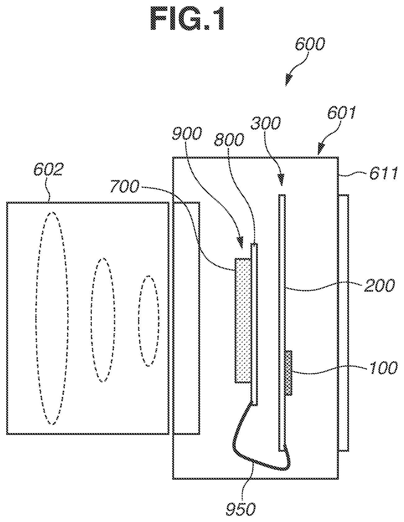
illustrates a digital camera 600 , an imaging apparatus as an example of an electronic apparatus according to a first exemplary embodiment. The digital camera 600 as an imaging apparatus is a lens exchangeable digital camera having a camera main body 601 . A lens unit (lens barrel) 602 including a lens is attachable to and detachable from the camera main body 601 . The camera main body 601 includes a housing 611 , a processing module 300 , and a sensor module 900 . The processing module 300 and the sensor module 900 are printed circuit boards disposed in the housing 611 . The processing module 300 is an example of a semiconductor module. The processing module 300 and the sensor module 900 are electrically connected with each other via a cable 950 .
The sensor module 900 includes an image sensor 700 and a printed wiring board 800 . The image sensor 700 is mounted on the printed wiring board 800 . The image sensor 700 is, for example, a complementary metal oxide semiconductor (CMOS) image sensor or a charge coupled device (CCD) image sensor. The image sensor 700 has a function of converting light incident via the lens unit 602 into an electrical signal.
The processing module 300 includes a semiconductor device 100 and a printed wiring board 200 as a first wiring board. The semiconductor device 100 is mounted on the printed wiring board 200 . The printed wiring board 200 is a rigid substrate. The semiconductor device 100 is, for example, a digital signal processor (DSP) having a function of acquiring an electrical signal from the image sensor 700 , subjecting the acquired electrical signal to correction processing, and generating image data.
The processing module 300 will now be described with reference to A to 4 .
The semiconductor device 100 is a semiconductor package with an area array. According to the first exemplary embodiment, the semiconductor device 100 is a semiconductor package with a ball grid array (BGA). The semiconductor device 100 includes a semiconductor element 101 and a package substrate 102 as a second printed wiring board. The package substrate 102 is a rigid substrate.
The semiconductor element 101 is mounted on the package substrate 102 . The package substrate 102 includes an insulating substrate 120 . The insulating substrate 120 has a main surface 121 , and a main surface 122 on the side opposite to the main surface 121 . The material of the insulating substrate 120 is ceramic such as alumina. The semiconductor element 101 is, for example, a semiconductor chip, and is mounted face up or face down. According to the first exemplary embodiment, the semiconductor element 101 is mounted face down on the main surface 121 of the insulating substrate 120 .
The semiconductor element 101 includes a plurality of power terminals, a plurality of ground terminals, and a plurality of signal terminals. Each terminal is bonded to the package substrate 102 by wire bonding or flip-chip bonding (not illustrated). B, 3 A, and 3 B illustrate a power terminal 111 E as one of the plurality of power terminals, and a ground terminal 111 G as one of the plurality of ground terminals. More specifically, the semiconductor element 101 includes the power terminal 111 E and the ground terminal 111 G.
The main surface 121 of the insulating substrate 120 is provided with a sealing resin 106 that seals the semiconductor element 101 . The package substrate 102 includes a plurality of lands 130 disposed on the main surface 122 of the insulating substrate 120 .
The plurality of lands 130 is arranged at minimum pitches of 0.7 mm or less. From the viewpoint of high-density land arrangements, it is desirable to arrange the lands 130 at minimum intervals of 0.4 mm or less. However, applicable patterns to be arranged include a lattice form (or a matrix form) and a hatched pattern. The lands 130 include terminals made of a conductive metallic material such as copper and gold. Examples of the lands 130 include signal terminals, power terminals, ground terminals, and dummy terminals. The plurality of lands 130 includes a land 130 E as a power terminal, a land 130 G as a ground terminal, and lands 130 S other than the lands 130 E and 130 G. The lands 130 S may be signal terminals, power terminals, ground terminals, and dummy terminals. The land 130 E is a first land, the land 130 G is a second land, and the lands 130 S include a plurality of third lands. The land 130 E as the first land and the land 130 G as the second land are adjacent to each other. The lands 130 S as the third lands are adjacent to the land 130 E as the first land and the land 130 G as the second land. The land 130 E is electrically connected to the power terminal 111 E of the semiconductor element 101 via a via conductor 112 E formed on the insulating substrate 120 . The land 130 G is electrically connected to the ground terminal 111 G of the semiconductor element 101 via a via conductor 112 G formed on the insulating substrate 120 .
A solder resist 108 is disposed on the main surface 122 . The solder resist 108 is a film made of a solder resist material. The plurality of lands 130 is respectively exposed from a plurality of openings formed on the solder resist 108 . The lands 130 may be either solder mask defined (SMD) lands or non-solder mask defined (NSMD) lands. According to the first exemplary embodiment, the lands 130 are SMD lands. The lands 130 may each be independently formed without using the solder resist 108 . Although not illustrated, a heat sink may be disposed on the top face of the semiconductor element 101 .
The printed wiring board 200 as a wiring board includes an insulating substrate 220 . The insulating substrate 220 includes a main surface 221 , and a main surface 222 on the side opposite to the main surface 221 . The printed wiring board 200 includes a plurality of lands 230 disposed on the main surface 221 of the insulating substrate 220 . The material of the insulating substrate 220 is an insulating material such as epoxy resin. However, the wiring board is not limited to a printed wiring board but may be a semiconductor substrate such as a silicon (Si) substrate.
The plurality of lands 230 includes terminals made of a conductive metallic material such as copper and gold. Examples of the lands 230 include signal terminals, power terminals, ground terminals, and dummy terminals. The material of the insulating substrate 220 is an insulating material such as epoxy resin. The plurality of lands 230 includes a land 230 E as a power terminal, a land 230 G as a ground terminal, and lands 230 S other than the lands 230 E and 230 G. The lands 230 S may be signal terminals, power terminals, ground terminals, or dummy terminals. The land 230 E is a fourth land, the land 230 G is a fifth land, and the lands 230 S include a plurality of sixth lands. The land 230 E as the fourth land and the land 230 G as the fifth land are adjacent to each other. The lands 230 S as the sixth lands are adjacent to the land 230 E as the fourth land and the land 230 G as the fifth land. The land 230 E is electrically connected to a via conductor 212 E formed on the insulating substrate 220 . The land 230 G is electrically connected to a via conductor 212 G formed on the insulating substrate 220 . A power integrated circuit (IC) (not illustrated) electrically connected to the via conductors 212 E and 212 G illustrated in B is mounted on the printed wiring board 200 . The power IC is capable of supplying power to the semiconductor element 101 of the semiconductor device 100 via first solder joints 191 and second solder joints 192 . A power IC (not illustrated) of the printed wiring board 200 may be electrically connected without using the via conductors 212 E and 212 G. The lands 230 S may be electrically connected to signal wirings (not illustrated). The land 230 E as the third land, the land 230 G as the fourth land, and the lands 230 S as the fifth lands are almost the same in size. More specifically, the area of the largest land of the fourth, the fifth, and the sixth lands is less than or equal to 1.1 times the area of the smallest land of the fourth, the fifth, and the sixth lands.
The printed wiring board 200 includes a solder resist 208 . The solder resist 208 is a film made of a solder resist material. The solder resist 208 is disposed on the main surface 221 . The plurality of lands 230 is respectively exposed from a plurality of openings formed on the solder resist 208 . The lands 230 may be either SMD lands or NSMD lands. According to the first exemplary embodiment, the lands 230 are SMD lands. The solder resist 208 may include a plurality of guiding portions 208 E and 208 G that cover a first conductor pattern 250 E and a second conductor pattern 250 G (described below), respectively. The function of the guiding portions 208 E and 208 G will be described below. The printed wiring board 200 does not need to include the solder resist 208 . In that case, the plurality of lands 230 may each be independently formed on the main surface 221 of the insulating substrate 220 . The openings of the solder resist 208 may expose the lands 230 S, 230 E, 230 G, and the region where a capacitor 400 is disposed.
According to the first exemplary embodiment, the land 230 E of the printed wiring board 200 is bonded to the land 130 E via the first solder joint 191 formed of solder. The land 230 G is bonded to the land 130 G via the second solder joint 192 formed of solder. The lands 230 S are bonded to the lands 130 S via third solder joints 193 formed of solder. Each solder joint may be described as “solder”.
The processing module 300 includes the capacitor 400 as an example of an electronic component. The capacitor 400 is a passive component and a chip component. It is desirable that the size of a chip component in a planar view is the 0402 size or smaller, for example the 0402 size (0.4 mm*0.2 mm) or the 0201 size (0.25 mm*0.125 mm). Notations, such as the 0402 size and the 0201 size, conform to the size notation method (based on mm) for electronic components in Japanese Industrial Standard (JIS).
The capacitor 400 includes an element 401 having a nearly rectangular parallelepiped shape extending longitudinally, and a pair of the electrodes 410 and 420 disposed on both sides of the element 401 across a distance in the longitudinal direction. A pair of the electrodes 410 and 420 are fixed to the element 401 across a distance in the longitudinal direction. Referring to B to 4 , the longitudinal direction of the capacitor 400 , i.e., the element 401 , is the X direction.
The widthwise direction of the capacitor 400 , i.e., the element 401 , is the Y direction. The Y direction is the width direction orthogonally intersecting with the X direction. The vertical direction of the capacitor 400 , i.e., the element 401 is the Z direction. The Z direction is the direction orthogonally intersecting with the X and Y directions. The Z direction is also orthogonal to the main surfaces 121 , 122 , 221 , and 222 .
One electrode 410 of a pair of the electrodes 410 and 420 is a first electrode, and the other electrode 420 thereof is a second electrode. The electrodes 410 and 420 each include an underground and a coating film that covers the underground. The material of the coating film of the electrodes 410 and 420 is a conductive metallic material such as tins.
The capacitor 400 is a bypass capacitor. The electrode 410 of the capacitor 400 is connected to the solder joint 191 . More specifically, the electrode 410 of the capacitor 400 is electrically connected to the lands 130 E and 230 E via the solder joint 191 . The electrode 420 of the capacitor 400 is connected to the solder joint 192 . More specifically, the electrode 420 of the capacitor 400 is electrically connected to the lands 130 G and 230 G via the solder joint 192 .
As illustrated in , the electrode 410 has three side faces 411 , 412 , and 413 , a top face 414 , and a bottom face 415 as electrode surfaces. The side faces 411 , 412 , and 413 , the top face 414 , and the bottom face 415 have a rectangular shape when viewed from the direction perpendicular to each surface. Two side faces 412 and 413 out of the three side faces 411 , 412 , and 413 face each other across a distance in the Y direction. The top face 414 and the bottom face 415 face each other across a distance in the Z direction. The side face 411 is perpendicular to and adjacent to the side faces 412 and 413 , the top face 414 , and the bottom face 415 . The electrode 420 has three side faces 421 , 422 , and 423 , a top face 424 , and a bottom face 425 as electrode surfaces. The side faces 421 , 422 , and 423 , the top face 424 , and the bottom face 425 have a rectangular shape when viewed from the direction perpendicular to each surface. Two side faces 422 and 423 out of three side faces 421 , 422 , and 423 face each other across a distance in the Y direction. The top face 424 and the bottom face 425 face each other across a distance in the Z direction. The side face 421 is perpendicular to and adjacent to the side faces 422 and 423 , the top face 424 , and the bottom face 425 . The side face 411 of the electrode 410 and the side face 421 of the electrode 420 are disposed to face each other across a distance in the X direction. The top face 414 of the electrode 410 faces the land 130 E of the semiconductor device 100 , and the bottom face 415 of the electrode 410 faces the land 230 E of the printed wiring board 200 . The top face 424 of the electrode 420 faces the land 130 G of the semiconductor device 100 , and the bottom face 425 of the electrode 420 faces the land 230 G of the printed wiring board 200 .
Power source noise is generated by the inductance of the wiring between the electrode 410 of the capacitor 400 and the power terminal 111 E and the inductance of the wiring between the electrode 420 of the capacitor 400 and the ground terminal 111 G. Power source noise is a voltage variation on the power line generated by the operation of the semiconductor device 100 . This voltage variation occurs when the power current is changed by the parasitic inductance and resistance on the power line. To reduce power source noise by reducing the inductance of the wiring, it is desirable to dispose the capacitor 400 such that the wiring distance between the power terminal 111 E and the ground terminal 111 G of the semiconductor device 100 is short. Since the electrode 410 of the capacitor 400 is electrically connected to the land 130 E of the semiconductor device 100 via the solder joint 191 , the inductance of the wiring between the electrode 410 of the capacitor 400 and the land 130 E can be reduced, according to the present disclosure. Since the electrode 420 of the capacitor 400 is electrically connected to the land 130 G of the semiconductor device 100 via the solder joint 192 , the inductance of the wiring between the electrode 420 of the capacitor 400 and the land 130 G can be reduced. The inductance of the wiring decreases to reduce power source noise, thereby achieving high-speed communication in the semiconductor device 100 .
Meanwhile, according to Japanese Patent Application Laid-Open No. 2020-205409, a capacitor as a chip component is solder-mounted between a semiconductor device and a wiring board. However, as a result of dedicated consideration by the inventor of the present application, it has been found that the technique disclosed in the above-described document does not provide a sufficient bonding strength between the chip component and solder.
More specifically, no solder ball of the semiconductor device is formed at the position where the chip component is connected. Thus, the volume of the solder joint connected with the electrode of the chip component is smaller than the volume of the solder joint that is connecting the semiconductor device and the wiring board. In the technique disclosed in Japanese Patent Application Laid-Open No. 2020-205409, the chip component sometimes comes off the solder joint when a strong impact, such as a drop test, is applied.
The present disclosure employs a configuration in which the volume of the first solder joint 191 and the volume of the second solder joint 192 are each larger than the volume of each third solder joint 193 . The inventor found that adopting such a configuration enables providing a higher bonding strength between the solder joints 191 and 192 and the capacitor 400 than the prior art. If the processing module 300 is applied with a strong impact such as a thermal shock, stress concentrates in the vicinity of the edges of the electrodes 410 and 420 of the capacitor 400 . If the volume of the solder joint 191 and the volume of the solder joint 192 are each smaller than the volume of each solder joint 193 , at least either one of the electrodes 410 and 420 of the capacitor 400 will come into contact with the land 130 or 230 . If stress concentrates in the vicinity of the edges of the electrodes 410 and 420 of the capacitor 400 in this state, a crack is likely to occur in the vicinity of the edges of the electrodes 410 and 420 . A crack may degrade the bonding reliability of the solder joints 191 and 192 with the capacitor 400 bonded thereto. In contrast, if the volume of the first solder joint 191 and the volume of the second solder joint 192 are each larger than the volume of each third solder joint 193 , stress applied to the edges of the electrode 410 and 420 of the capacitor 400 can be dispersed. Thus, the possibility of occurring of the above-described crack decreases, and the bonding reliability improves.
More desirably, the volume of the first solder joint 191 and the volume of the second solder joint 192 are each more than or equal to 1.2 times the volume of each third solder joint 193 . It is desirable that the volume of the first solder joint 191 and the volume of the second solder joint 192 are each less than four time the volume of each third solder joint 193 . If the volume of the first solder joint 191 and the volume of the second solder joint 192 are each more than or equal to four times the volume of each third solder joint 193 , solder joints cannot be disposed at narrow pitches, and there may be a possibility that the semiconductor device 100 cannot be reduced in size.
It is desirable that the capacitor 400 is disposed across a void with each of the semiconductor device 100 and the printed wiring board 200 . It is desirable that the electrode 410 of the capacitor 400 is separated from the land 130 E of the semiconductor device 100 and the land 230 E of the printed wiring board 200 and that the electrode 420 of the capacitor 400 is separated from the land 130 G of the semiconductor device 100 and the land 230 G of the printed wiring board 200 . More specifically, it is desirable that the difference between the first distance from the capacitor 400 to the semiconductor device 100 and the second distance from the capacitor 400 to the printed wiring board 200 is smaller than the first and the second distances and is close to zero. More specifically, it is desirable that the capacitor 400 is disposed at the centers of the solder joints 191 and 192 . If the capacitor 400 is disposed at the center between the solder joints 191 and 192 , stress applied to the edges of the electrodes 410 and 420 of the capacitor 400 can be dispersed. This reduces the impact on the capacitor 400 , making it possible to further improve the bonding reliability.
As illustrated in A , a maximum length R 191 of the solder joint 191 in the X direction is larger than a maximum length R 193 of each solder joint 193 in the X direction. However, if the maximum length of the solder joint 191 in the X direction is long, the solder joint 191 may possibly come into contact with the solder joints 193 to cause a short-circuit. Thus, it is desirable that the maximum length of the solder joint 191 in the X direction is twice the maximum length or less of each solder joint 193 in the X direction.
It is desirable that the processing module 300 includes a first chip component guiding path 260 E and a second chip component guiding path 260 G. The first chip component guiding path 260 E and the second chip component guiding path 260 G guide the capacitor 400 to the solder joints 191 and 192 , respectively, when the processing module 300 is manufactured. WO 2005/024945 discloses a technique of providing a solder paste on a footprint extending in the widthwise direction of the capacitor as a chip component, disposing and heating the capacitor on the solder paste, and guiding and bonding the capacitor up to metal bumps. However, after a consideration by the inventor of the present disclosure, it was found that the technique discussed in WO 2005/024945 may have a difficulty in repetitively disposing the chip component at the same position with favorable reproducibility. According to WO 2005/024945, the foot printing serving as the conductor pattern according to the present embodiment is exposed on a substrate, and a step is generated between a land and the substrate surface. The chip component may therefore be caught by the step and then widthwisely rotated. If the chip component is bonded while rotating, a unique point occurs where stress is concentrated after the bonding, resulting in an insufficient bonding strength.
The first chip component guiding path 260 E as a first component guiding path includes the first conductor pattern 250 E, and the guiding portion 208 E of the solder resist for covering the first conductor pattern 250 E.
The first conductor pattern 250 E extends from the land 230 E disposed on the main surface 221 of the insulating substrate 220 , in a first direction intersecting with the longitudinal direction of the capacitor 400 . The length in the Y direction is larger than a half of the widthwise length of the capacitor 400 and is shorter than the shortest distance between the land 230 E as the third land and the lands 230 S as the fifth lands. The first conductor pattern 250 E is out of contact with the lands 230 G and 230 S. The first conductor pattern 250 E is not directly connected with a wiring (not illustrated).
The second chip component guiding path 260 G as the second component guiding path includes the second conductor pattern 250 G, and the guiding portion 208 G of the solder resist for covering the second conductor pattern 250 G.
The second conductor pattern 250 G extends from the land 230 G disposed on the main surface 221 of the insulating substrate 220 , in a second direction intersecting with the longitudinal direction of the capacitor 400 . The length in the Y direction is larger than a half of the widthwise length of the capacitor 400 and is shorter than the shortest distance between the land 230 G as the fourth land and the lands 230 S as the fifth lands. The second conductor pattern 250 G is out of contact with the lands 230 E and 230 S. The second conductor pattern 250 G is not directly connected with a wiring (not illustrated).
The first conductor pattern 250 E extends from the land 230 E in a direction approaching the second conductor pattern 250 G. However, the first conductor pattern 250 E and the second conductor pattern 250 G may extend in parallel. This means that the first and the second directions may be the same. The first conductor pattern 250 E and the second conductor pattern 250 G are formed of a conductive metallic material, e.g., copper or gold. Although the first conductor pattern 250 E and the second conductor pattern 250 G have a rectangular shape when viewed in the Z direction, the present disclosure is not limited thereto. These conductor patterns may have any shape, such as a polygon shape, circular shape, and elliptic shape.
When bonding the capacitor 400 as a chip component with the first solder joint 191 and the second solder joint 192 , the first chip component guiding path 260 E and the second chip component guiding path 260 G guide the capacitor 400 to the bonding portion. Solder pastes are placed on the guiding portions 208 E and 208 G, and the capacitor 400 is disposed on the solder pastes. When the solder pastes are heated and melted, the capacitor 400 is guided to the bonding portion.
In the first chip component guiding path 260 E and the second chip component guiding path 260 G, the first conductor pattern 250 E and the second conductor pattern 250 G are covered by the guiding portions 208 E and 208 G of the solder resist, respectively. Adopting this configuration enables horizontally moving the mounted capacitor 400 while maintaining its orientation. This is because there arises no step until the capacitor 400 is guided from the first chip component guiding path 260 E and the second chip component guiding path 260 G to the bonding portion. As a result, the center line connecting the centers of the solder joints 191 and 192 and the longitudinal center line of the capacitor 400 are positioned on the same line, as illustrated in C , to facilitate bonding.
It is desirable that the length of the first conductor pattern 250 E and the length of the second conductor pattern 250 G are each larger than a half of the widthwise length of the capacitor 400 . This enables placing sufficient amounts of solder pastes to stably guide the capacitor 400 . It is desirable that the first conductor pattern 250 E extends from the land 230 E in a direction approaching the second conductor pattern 250 G. By mounting the first conductor pattern 250 E and the second conductor pattern 250 G in such a way, these patterns can be further extended. It is also desirable that the width of the first conductor pattern 250 E and the width of the second conductor pattern 250 G are each at least the width of the electrode of the capacitor 400 . This prevents the capacitor 400 from falling off the guiding paths and enables stably moving the capacitor 400 . The width of the electrode of the capacitor 400 is the length of the bottom face 415 of the capacitor 400 or the length of the bottom face 425 of the capacitor 400 , in the X direction in .
When the above-described process for heating and melting solder pastes is performed, a flux F 1 remains on the guiding portion 208 E, and a flux F 2 on the guiding portion 208 G. It is desirable that the fluxes F 1 and F 2 are provided only on the guiding portions 208 E and 208 G, respectively. This is intended to prevent an ion migration phenomenon that occurs when fluxes remaining on the guiding paths come into contact with each other or come into contact with a neighboring flux.
The above-described disclosure can provide a semiconductor module having a sufficient bonding strength between solder and a capacitor to a further extent than the prior art. The above-described disclosure can also provide a semiconductor module in which the layout of the bypass capacitor is controlled with a high accuracy.
(Processing Module Manufacturing Method 1)
A method of manufacturing a processing module 300 will now be described. A to 5 D and 6 A to 6 C illustrate the method of manufacturing the processing module 300 according to a first exemplary embodiment. A side view and a top view are illustrated for each step.
As illustrated in A , a printed wiring board 200 is prepared (Step S 1 ). The printed wiring board 200 includes the lands 230 E, 230 G, and 230 S, the first conductor pattern 250 E, the second conductor pattern 250 G, and the solder resist 208 on the main surface 221 . The solder resist 208 is provided with the guiding portions 208 E and 208 G, and a plurality of openings. The lands 230 E, 230 G, and 230 S are exposed from the openings of the solder resist 208 . In step S 1 , the semiconductor device 100 and the capacitor 400 are prepared.
As illustrated in B , a solder paste P 1 as a first solder paste, a solder paste P 2 as a second solder paste, and solder pastes P 3 as third solder pastes are supplied across a distance between them on the printed wiring board 200 (Step S 2 ).
The solder paste P 1 is supplied onto the land 230 E as the third land and the guiding portion 208 E. The solder paste P 2 is supplied onto the land 230 G as a fourth land and the guiding portion 208 G. The solder pastes P 3 are supplied onto the lands 230 S as fifth lands.
The solder pastes P 1 , P 2 and P 3 contain solder powder and flux components used for soldering. Although, in the present disclosure, the solder pastes P 1 , P 2 and P 3 are made of the same material, the solder pastes may not be made of the same material as long as the temperatures of their melting points are close. In step S 2 , the solder pastes P 1 , P 2 and P 3 are supplied to the printed wiring board 200 through screen printing using a metal mask 23 . The method for supplying the solder pastes P 1 , P 2 , and P 3 is not limited thereto. For example, a dispenser may be used.
As illustrated in C , the capacitor 400 is mounted such that the electrode 410 comes into contact with the solder paste P 1 on the guiding portion 208 E, and the electrode 420 comes into contact with the solder paste P 2 on the guiding portion 208 G. More specifically, on the solder pastes P 1 and P 2 provided on the guiding portions 208 E and 208 G, the capacitor 400 is mounted in the vicinity of the tips in a direction away from the lands 230 E and 230 G, respectively (Step S 3 ). Thus, the bottom face 415 of the electrode 410 comes into contact with the solder paste P 1 , and the bottom face 425 of the electrode 420 comes into contact with the solder paste P 2 . In step S 3 , the capacitor 400 is mounted on the solder pastes P 1 and P 2 by using a mounter (not illustrated).
As illustrated in D , the semiconductor device 100 is mounted on the printed wiring board 200 so that the land 130 E faces the land 230 E, and the land 130 G faces the land 230 G (Step S 4 ). In step S 4 , the semiconductor device 100 is mounted on the printed wiring board 200 by using a mounter (not illustrated). In this case, the mounting position of the semiconductor device 100 is adjusted such that the land 130 E faces the land 230 E, the land 130 G faces the land 230 G, and the lands 130 S face the lands 230 S. The lands 130 E, 130 G, and 130 S of the semiconductor device 100 are provided with solder balls B 1 , B 2 , and B 3 , respectively. Thus, the semiconductor device 100 is mounted on the printed wiring board 200 such that the solder balls B 1 , B 2 , and B 3 face the lands 230 E, 230 G, and 230 S, respectively. In step S 4 , when the semiconductor device 100 is mounted on the printed wiring board 200 , the solder balls B 1 , B 2 , and B 3 come into contact with the solder pastes P 1 , P 2 , and P 3 , respectively. In step S 4 , the positional relations between the printed wiring board 200 , the capacitor 400 , and the semiconductor device 100 are as illustrated in D when viewed from the Z direction. The lands 130 E, 130 G, and 130 S of the semiconductor device 100 are each partly or entirely overlapped with the lands 230 E, 230 G, and 230 S of the printed wiring board 200 , respectively, when viewed from the Z direction. When the semiconductor device 100 is mounted, the capacitor 400 is mounted at a position that is out of contact with the solder balls B 1 and B 2 . The top view in D illustrates only the solder balls B 1 , B 2 , and B 3 out of the configurations of the semiconductor device 100 .
Then, in a state where the semiconductor device 100 and the capacitor 400 are mounted on the printed wiring board 200 , these components are conveyed to a reflow furnace (not illustrated). In step S 5 illustrated in A , the temperature of the atmosphere in the reflow furnace is adjusted to the temperature of the melting point of the solder powder or higher, and then the solder pastes P 1 , P 2 , and P 3 and the solder balls B 1 , B 2 , and B 3 are heated and melted. When the solder paste P 1 and the solder ball B 1 are melted, a fluid molten solder M 1 is formed. When the solder paste P 2 and the solder ball B 2 are melted, a fluid molten solder M 2 is formed. When the solder pastes P 3 and the solder balls B 3 are melted, fluid molten solders M 3 are formed.
In step S 6 illustrated in B , following step S 5 , heating is continued to fluidize the molten solders M 1 and M 2 . The molten solders M 1 and M 2 on the guiding portions 208 E and 208 G are agglomerated on the lands 230 E and 230 G, respectively. Thus, the capacitor 400 mounted on the guiding portions 208 E and 208 G reaches the lands 230 E and 230 G through the agglomeration of the molten solders M 1 and M 2 , respectively. When the capacitor 400 reaches the lands 230 E and 230 G, the capacitor 400 is raised in an upper direction approaching the semiconductor device 100 by the force received from the molten solders M 1 and M 2 , respectively.
As a result, the distance between the top face 414 of the electrode 410 and the 130 E decreases, and the distance between the top face 424 of the electrode 420 and the land 130 G also decreases. More specifically, the element 401 of the capacitor 400 is disposed across a void with each of the semiconductor device 100 and the printed wiring board 200 . Then, the fluxes F 1 and F 2 contained in the solder pastes P 1 and P 2 remain on the chip component guiding paths 260 E and 260 G, respectively.
Thereafter, the molten solders M 1 , M 2 , and M 3 are cooled for solidification. As illustrated in C , the solder joint 191 as the first solder joint is formed where the lands 130 E and 230 E and the electrode 410 are bonded with solder. The solder joint 192 as the second solder joint is formed where the lands 130 G and 230 G and the electrode 420 are bonded with solder. The solder joints 193 as the third solder joints are formed where the lands 130 S and 230 S are bonded with solder. In this case, the volume of the solder joint 191 and the volume of the solder joint 192 are each larger than the volume of each solder joint 193 . Although the solder balls B 1 , B 2 , and B 3 are fixed in size, the paste P 1 placed on the guiding portion 208 E adheres to the solder ball B 1 and then solidifies, and the paste P 2 placed on the guiding portion 208 G adheres to the solder ball B 2 and then solidifies. More specifically, the volumes of the solder joints 191 and 192 can be controlled by the amounts of the solder pastes P 1 and P 2 to be placed on the guiding portions 208 E and 208 G, respectively. The processing module 300 illustrated in A to 3 C is manufactured by the above-described processes.
Subsequently, the camera main body 601 , i.e., the digital camera 600 , is manufactured by storing the processing module 300 in the housing 611 illustrated in .
The manufacturing method according to the present disclosure makes it possible to manufacture the processing module 300 in which the volume of the solder joint 191 and the volume of the solder joint 192 for bonding the capacitor 400 are each larger than the volume of each solder joint 193 for bonding the semiconductor device 100 and the wiring board 200 . The manufacturing method of the present disclosure can therefore provide a semiconductor module having a sufficient bonding strength between solder and the capacitor 400 to a further extent than the prior art. The capacitor 400 as a chip component is guided to the bonding portion by the first chip component guiding path 260 E and the second chip component guiding path 260 G. The manufacturing method of the present disclosure can thus provide a semiconductor module manufacturing method that enables controlling the layout of the bypass capacitor with higher accuracy than the prior art. The capacitor 400 is disposed across a void with each of the semiconductor device 100 and the printed wiring board 200 . Thus, bonding is made in a solder bonding form that is axisymmetric with reference to the straight line connecting the centers of the solder joints 191 and 192 . This improves the bonding reliability of the processing module 300 since no unique point occurs where stress is concentrated after the bonding.
(Processing Module Manufacturing Method 2)
A second method of manufacturing a processing module as a modification of the above-described manufacturing method will now be described. A to 7 D and 8 A to 8 C illustrate a method of manufacturing a processing module 300 A. The processing module 300 A differs from the processing module 300 in that the printed wiring board 200 is not provided with the first chip component guiding path 260 E and the second chip component guiding path 260 G.
As illustrated in A , a printed wiring board 200 is prepared (Step S 11 ). The printed wiring board 200 includes lands 230 EA, 230 GA, and 230 SA, and the solder resist 208 having a plurality of openings on the main surface 221 A. The lands 230 E, 230 G, and 230 S are exposed from the openings of the solder resist 208 . In step S 11 , the semiconductor device 100 and the capacitor 400 are prepared. On the semiconductor device 100 , the solder balls B 1 , B 2 , and B 3 as ball terminals are attached to the lands 130 E, 130 G, and 130 S, respectively, in advance so that the center of each solder ball coincides with the center of each land 230 . According to the present exemplary embodiment, it is desirable that the solder balls B 1 , B 2 , and B 3 are the same in size and material. However, the solder balls are not limited to the same size and the same material as long as the temperatures of their melting points are close.
As illustrated in B , the solder paste P 1 as the first solder paste, the solder paste P 2 as the second solder paste, and the solder pastes P 3 as the third solder pastes are supplied across a distance between them on the printed wiring board 200 (Step S 12 ).
The solder paste P 1 extends from the land 230 E as the fourth land, and is also supplied onto the solder resist 208 . The solder paste P 2 is also supplied onto the solder resist 208 extending from the land 230 GA as the fifth land. The solder pastes P 3 are supplied onto the lands 230 A as the sixth lands.
The solder pastes P 1 , P 2 , and P 3 contain solder powder and flux components used for soldering. In the present disclosure, the solder pastes P 1 , P 2 , and P 3 are made of the same material. However, the solder pastes do not need to be made of the same material as long as the temperatures of their melting points are close. In step S 2 , the solder pastes P 1 , P 2 and P 3 are supplied to the printed wiring board 200 through screen printing using a metal mask 23 . The method of supplying the solder pastes P 1 , P 2 , and P 3 is not limited thereto. For example, a dispenser may be used.
The volumes of the solder joints 191 and 192 are controllable by using the amounts of the solder pastes P 1 and P 2 .
The capacitor is then mounted such that the electrodes 410 and 420 come into contact with the solder pastes P 1 and P 2 , respectively (Step S 13 ), as illustrated in C . The bottom face 415 of the electrode 410 thereby comes into contact with the solder paste P 1 , and the bottom face 425 of the electrode 420 comes into contact with the solder paste P 2 . In step S 13 , the capacitor 400 is mounted on the solder pastes P 1 and P 2 by using a mounter (not illustrated).
The semiconductor device 100 is then mounted on the printed wiring board 200 so that the lands 130 S face the lands 230 SA, the land 130 E faces the land 230 EA, and the land 130 G faces the land 230 GA (Step S 14 ). In step S 14 , the semiconductor device 100 is mounted on the printed wiring board 200 by using a mounter (not illustrated). In this case, the mounting position of the semiconductor device 100 is adjusted such that the land 130 E faces the land 230 EA, the land 130 G faces the land 230 GA, and the lands 130 S face the lands 230 SA. The lands 130 E, 130 G, and 130 S of the semiconductor device 100 are provided with the solder balls B 1 , B 2 , and B 3 , respectively. Thus, the semiconductor device 100 is mounted on the printed wiring board 200 such that the solder ball B 1 faces the land 230 EA, the solder ball B 2 faces the land 230 GA, and the solder balls B 3 face the lands 230 SA. In step S 14 , when the semiconductor device 100 is mounted on the printed wiring board 200 , the solder balls B 1 , B 2 , and B 3 come into contact with the solder pastes P 1 , P 2 , and P 3 , respectively. In step S 14 , the positional relations between the printed wiring board 200 , the capacitor 400 , and the semiconductor device 100 are as illustrated in D when viewed from the Z direction. The lands 130 E, 130 G, and 130 S of the semiconductor device 100 are each partially or entirely overlapped with the lands 230 EA, 230 GA, and 230 SA of the printed wiring board 200 , respectively, when viewed from the Z direction. When the semiconductor device 100 is mounted, the capacitor 400 is mounted at a position that is out of contact with the solder balls B 1 and B 2 .
These components are then conveyed to a reflow furnace (not illustrated) in a state where the semiconductor device 100 and the capacitor 400 are mounted on the printed wiring board 200 . In step S 15 illustrated in A , the temperature of the atmosphere in the reflow furnace is adjusted to the temperature of the melting point of the solder powder or higher, and then the solder pastes P 1 , P 2 , and P 3 and the solder balls B 1 , B 2 , and B 3 are heated and melted.
When the solder paste P 1 and the solder ball B 1 are melted, a fluid molten solder M 191 is formed as a result of agglomeration. When the solder paste P 2 and the solder ball B 2 are melted, a fluid molten solder M 192 is formed as a result of agglomeration. When the solder pastes P 3 and the solder balls B 3 are melted, fluid molten solders M 193 are formed as a result of agglomeration.
In this case, there is a relation W 1 >W 2 , where W 1 denotes the solder wettability on the lands 230 EA and 230 G of the printed wiring board 200 , and W 2 denotes the solder wettability on the solder resist 208 of the printed wiring board 200 . Thus, the solder paste P 1 on the solder resist 208 is agglomerated toward the solder paste P 1 and the solder ball B 1 between the lands 130 E and 230 EA having the best solder wettability, and then is integrally formed as the molten solder M 191 . The solder paste P 2 on the solder resist 208 is agglomerated toward the solder paste P 2 between the lands 130 G and 230 E having the highest solder wettability, and then is integrally formed as the molten solder M 192 .
There is a relation W 3 >W 2 , where W 3 denotes the solder wettability on the electrode surfaces 411 , 412 , 413 , 414 , 415 , 421 , 422 , 423 , 424 , and 425 of the capacitor 400 . Thus, the solder pastes melted on the electrode surfaces 411 , 412 , 413 , 414 , 415 , 421 , 422 , 423 , 424 , and 425 of the capacitor 400 get wet, and are covered by solder. Since the electrodes 410 and 420 of the capacitor 400 are covered by solder, the capacitor 400 moves in the Y1 direction of the lands 230 EA and 230 GA with the flows of the solder pastes P 1 and P 2 . Then, the electrodes 410 and 420 of the capacitor 400 are brought in by the molten solders M 191 and M 192 .
The volume of the molten solder M 191 and the volume of the molten solder M 192 each become larger than the volume of each molten solder M 193 by the volume of agglomeration of the solder pastes P 1 and P 2 , respectively.
In step S 16 illustrated in B , following step S 15 , heating is continued to further fluidize the molten solders M 191 , M 192 , and M 193 to make the solders spherical. When the molten solders become spherical, the electrodes 410 and 420 of the capacitor 400 are induced in the X1 and X2 directions at the solder joints 191 and 192 , respectively, by a substantially equal force. Thus, the capacitor 400 is subjected to self-alignment to the vicinity of the centers of the solder joints 191 and 192 in the X and Y directions. Also, the electrodes 410 and 420 are induced in the X1 and X2 directions at the solder joints 191 and 192 , respectively, by a substantially equal force and, at the same time, are also induced in the Z1 and Z2 directions at the solder joints 191 and 192 , respectively, by a substantially equal force. Thus, a void is formed between the capacitor 400 and the semiconductor device 100 and between the capacitor 400 and the printed wiring board 200 .
When the solder volume is large and the solder shape is close to sphericity, the difference between the first distance from the capacitor 400 to the semiconductor device 100 and the second distance from the capacitor 400 to the printed wiring board 200 is smaller than the first and the second distances and is close to zero. In other words, the capacitor 400 can be disposed at the centers of the solder joints 191 and 192 .
Subsequently, the molten solders M 191 , M 192 , and M 193 are cooled for solidification. As illustrated in C , the solder joint 191 is formed where the land 130 E, the electrode 410 , and the land 230 EA are bonded with solder. The solder joint 192 is formed where the land 130 G, the electrode 420 , and the land 230 GA are bonded with solder. The solder joints 193 are formed where the lands 130 S and 230 SA are bonded with solder. The processing module 300 A is manufactured by the above-described processes.
Thereafter, the processing module 300 A is stored in the housing 611 illustrated in , and the camera main body 601 , i.e., the digital camera 600 , is manufactured.
The manufacturing method of the present disclosure makes it possible to manufacture the processing module 300 in which the volume of the solder joint 191 and the volume of the solder joint 192 for bonding the capacitor 400 are each larger than the volume of each solder joint 193 for bonding the semiconductor device 100 and the wiring board 200 . The manufacturing method of the present disclosure can therefore provide a semiconductor module having a sufficient bonding strength between solder and the capacitor 400 to a further extent than the prior art.
A first sample corresponding to the first exemplary embodiment will now be described. On the semiconductor device 100 illustrated in C , the minimum pitch between the solder balls B as two adjacent ball terminals before the bonding was 0.4 mm (millimeters). The size of the solder balls B was ϕ0.25 mm. The material of the land 130 was Cu. The material of the solder balls B was Sn-3.0% Ag0.5% Cu. The area of the capacitor 400 when viewed from the Z direction was 0.2 mm*0.1 mm. The capacitor 400 was a chip component of the 0201 size.
The size of the lands 130 E and 130 G on the semiconductor device 100 was ϕ0.22 mm when viewed from the Z direction. The size of the lands 230 E and 230 G on the printed wiring board 200 when viewed from the Z direction was ϕ0.22 mm which was the same as the size of the lands 130 E and 130 G. The pitch of the lands 230 was 0.4 mm.
In step S 12 illustrated in B , the solder pastes P 1 and P 2 were 0.22 mm in width, and were extended from the solder paste on the lands 230 E and 230 G to the length of 0.25 mm. The thickness of a metal mask 23 was 0.08 mm decided based on the minimum pitch between the solder balls B as two adjacent ball terminals before bonding and the size of the capacitor 400 on the semiconductor device 100 .
The solder pastes P 1 , P 2 , and P 3 were made of a material containing solder powder of Sn-3.0% Ag0.5% Cu and a flux component.
In steps S 15 and S 16 illustrated in A and 8 B , respectively, the peak temperature of the atmosphere in the reflow furnace was set to 230° C. or higher to melt the solder balls B 1 , B 2 , and B 3 and the solder pastes P 1 , P 2 , and P 3 . Subsequently, the molten solders M 191 , M 192 , and M 193 were cooled for solidification. It was confirmed that the capacitor 400 was bonded to the semiconductor device 100 by the spherical solder joints 191 and 192 .
On the manufactured processing module, the volume of the solder joint 191 and the volume of the solder joint 192 were each 1.2 times the volume of each solder joint 193 . The maximum width of the solder joint 191 and the maximum width of the solder joint 192 were each 7% larger than the maximum width of each solder joint 193 . A void was formed between the capacitor 400 and the semiconductor device 100 and between the capacitor 400 and the printed wiring board 200 . Further, a flux trace was confirmed to be on the solder resist 208 at positions where the solder pastes P 1 and P 2 were screen-printed.
A second exemplary embodiment will now be described. The second exemplary embodiment is an exemplary embodiment when the capacitor 400 is disposed to build a bridge to the land disposed in the outermost periphery out of the lands disposed on the semiconductor device 100 . A to 9 C are cross-sectional view schematically illustrating an enlarged part of the processing module according to the second exemplary embodiment. A is a cross-sectional view schematically illustrating the processing module 300 A according to the second exemplary embodiment. B is a cross-sectional view taken along the B 2 -B 2 line illustrated in A . C is a cross-sectional view taken along the C 2 -C 2 line illustrated in A . A and 9 B schematically illustrate a layout relation between the semiconductor device 100 , the capacitor 400 , and the printed wiring board 200 A. In the following descriptions, configurations similar to those in the first exemplary embodiment are assigned the same reference numerals, and detailed descriptions thereof will be omitted.
The processing module 300 A according to the second exemplary embodiment includes the semiconductor device 100 and the printed wiring board 200 A having a similar configuration to the first exemplary embodiment. Similarly to the first exemplary embodiment, the lands 130 E, 130 G, and 130 S are disposed on the main surface 122 of the insulating substrate 120 included in the semiconductor device 100 .
The printed wiring board 200 A includes an insulating substrate 220 A. The insulating substrate 220 A includes a main surface 221 A, and a main surface 222 A on the side opposite to the main surface 221 A. The printed wiring board 200 A includes, on the main surface 221 A, the land 230 EA as the fourth land, the land 230 GA as the fifth land, the lands 230 SA as the sixth lands, a first conductor pattern 250 EA, and a second conductor pattern 250 GA.
The printed wiring board 200 A includes a solder resist 208 A as a film made of a solder resist material. The solder resist 208 A is disposed on the main surface 221 A. The lands 230 EA, 230 GA, and 230 SA are exposed from a plurality of openings formed on the solder resist 208 A. The solder resist 208 A includes a plurality of guiding portions 208 EA and 208 GA that cover the first conductor pattern 250 EA and the second conductor pattern 250 GA, respectively (described below).
The lands 130 E and 230 EA are bonded by a solder joint 191 A as a first solder joint formed of solder. The lands 130 G and 230 GA are bonded by a solder joint 192 A as a second solder joint formed of solder. The lands 130 S and 230 SA are bonded by solder joints 193 A as third solder joints formed of solder.
Similarly to the first exemplary embodiment, the processing module 300 A includes the capacitor 400 to be used as a bypass capacitor. The capacitor 400 is disposed on the main surface 221 A of the insulating substrate 220 A of the printed wiring board 200 A, i.e., between the semiconductor device 100 and the printed wiring board 200 A. The electrode 410 of the capacitor 400 is connected to the solder joint 191 A. More specifically, the electrode 410 of the capacitor 400 is electrically connected to the lands 130 E and 230 EA via the solder joint 191 A. The electrode 420 of the capacitor 400 is connected to the solder joint 192 A. More specifically, the electrode 420 of the capacitor 400 is electrically connected to the lands 130 G and 230 GA via the solder joint 192 A.
The processing module 300 A includes a first chip component guiding path 260 EA and a second chip component guiding path 260 GA. The first chip component guiding path 260 EA and the second chip component guiding path 260 GA guides the capacitor 400 to the solder joints 191 A and 192 A, respectively, when manufacturing the processing module 300 A.
The first chip component guiding path 260 EA as the first component guiding path includes the first conductor pattern 250 EA, and the guiding portion 208 EA of the solder resist for covering the first conductor pattern 250 EA. The first conductor pattern 250 EA extends from the land 230 EA disposed on the main surface 221 A of the insulating substrate 220 A in the first direction that intersects with the longitudinal direction of the capacitor 400 .
The length of the first conductor pattern 250 EA in the Y direction is larger than a half of the widthwise length of the capacitor 400 . When the processing module 300 is planarly viewed from the side of the semiconductor device 100 (when viewed from the top surface), the end of the first conductor pattern 250 EA on the side not connecting with the land 230 EA extends to the outside of the semiconductor device 100 . The first conductor pattern 250 EA is out of contact with the lands 230 SA. The first conductor pattern 250 EA is not directly connected to a wiring (not illustrated).
The second chip component guiding path 260 GA as the second component guiding path includes the second conductor pattern 250 GA, and the guiding portion 208 GA of the solder resist for covering the second conductor pattern 250 GA. The second conductor pattern 250 GA extends from the land 230 GA disposed on the main surface 221 A of the insulating substrate 220 A in the second direction that intersects with the longitudinal direction of the capacitor 400 .
The length of the second conductor pattern 250 GA in the Y direction is larger than a half of the widthwise length of the capacitor 400 . When the processing module 300 is viewed from the top surface, the end of the second conductor pattern 250 GA on the side not connecting with the land 230 GA extends to the outside of the semiconductor device 100 . The second conductor pattern 250 GA is out of contact with the lands 230 SA. The second conductor pattern 250 GA is not directly connected to a wiring (not illustrated).
The first conductor pattern 250 EA extends from the land 230 EA in a direction approaching the second conductor pattern 250 G. However, the first conductor pattern 250 E and the second conductor pattern 250 G may extend in parallel. This means that the first and the second directions can be the same. The first conductor pattern 250 EA and the second conductor pattern 250 GA are formed of a conductive metallic material, e.g., copper or gold.
When bonding the capacitor 400 as a chip component with the solder joints 191 A and 192 A, the first chip component guiding path 260 EA and the second chip component guiding path 260 GA guides the capacitor 400 to the bonding portion, respectively. Solder pastes are placed on the guiding portions 208 EA and 208 GA and the capacitor 400 is disposed on the solder pastes. When the solder pastes are heated and melted, the capacitor 400 is guided to the bonding portion.
According to the second exemplary embodiment, the first chip component guiding path 260 EA and the second chip component guiding path 260 GA are extended to the outside of the semiconductor device 100 , as illustrated in B . By extending the chip component guiding paths 260 EA and 260 GA to the outside of the semiconductor device 100 , the capacitor 400 can be mounted outside the semiconductor device 100 . Mounting the capacitor 400 outside the semiconductor device 100 enables a visual inspection after the parts mounting.
The length of the first conductor pattern 250 EA and the length of the second conductor pattern 250 GA are each larger than a half of the widthwise length of the capacitor 400 , thereby making it possible to place sufficient amounts of solder pastes to stably guide the capacitor 400 . It is desirable that the first conductor pattern 250 E extends from the land 230 E in a direction approaching the second conductor pattern 250 G. This is because mounting the first conductor pattern 250 EA and the second conductor pattern 250 GA in this way enables these patterns to extend further. It is desirable that the width of the first conductor pattern 250 EA and the width of the second conductor pattern 250 GA are more than or equal to the widths of the electrodes of the capacitor 400 . This prevents the capacitor 400 from falling off the guiding paths to stably move the capacitor 400 .
When the above-described process for heating and melting solder pastes is performed, the flux F 1 remains on the guiding portion 208 EA, and the flux F 2 remains on the guiding portion 208 GA.
It is desirable that the fluxes F 1 and F 2 are provided only on the guiding portions 208 EA and 208 GA. This is intended to prevent an ion migration phenomenon that occurs when fluxes remaining on the guiding paths come into contact with each other or come into contact with a neighboring flux.
It is desirable that the volume of the first solder joint 191 A and the volume of the second solder joint 192 A are each larger than the volume of each third solder joint 193 A. Adopting such a configuration makes it easier to control the layout of the capacitor 400 with a high accuracy. More desirably, the volume of the first solder joint 191 A and the volume of the second solder joint 192 A are more than 1.2 times the volume of each third solder joint 193 A. It is also desirable that the volume of the first solder joint 191 A and the volume of the second solder joint 192 A are each less than four times the volume of each third solder joint 193 A. If the volume of the first solder joint 191 A and the volume of the second solder joint 192 A are more than or equal to four times the volume of each third solder joint 193 , solder joints cannot be placed at narrow pitches, and the semiconductor device 100 may not possibly be reduced in size.
Regarding the processing module 300 A, the capacitor 400 can be connected to the solder joints by using component guiding paths having two different conductor patterns covered by the guiding portions of the solder resist. The above-described disclosure can thereby provide a semiconductor module in which the layout of the bypass capacitor is controlled with higher accuracy than the prior art.
(Processing Module Manufacturing Method 3)
A method of manufacturing the processing module 300 A will now be described. A to 10 D and 11 A to 11 C illustrate a method for manufacturing the processing module 300 A according to the second exemplary embodiment. A side view and a top view are illustrated for each step.
As illustrated in A , the printed wiring board 200 A is prepared (Step S 21 ).
The printed wiring board 200 A includes the lands 230 EA, 230 GA, and 230 SA, the first conductor pattern 250 EA, the second conductor pattern 250 GA, and the solder resist 208 A on the main surface 221 A. The solder resist 208 A is provided with the guiding portions 208 EA and 208 GA, and a plurality of openings. The lands 230 EA, 230 GA, and 230 SA are exposed from the openings of the solder resist 208 A. In step S 11 , the semiconductor device 100 and the capacitor 400 are also prepared.
As illustrated in B , the solder paste P 1 as the first solder paste, the solder paste P 2 as the second solder paste, and the solder pastes P 3 as the third solder pastes are supplied across a distance from each other on the printed wiring board 200 A (Step S 22 ). The solder paste P 1 is supplied onto the land 230 EA as the third land and onto the guiding portion 208 EA. The solder paste P 2 is supplied onto the land 230 GA as the fourth land and onto the guiding portion 208 GA. The solder pastes P 3 are supplied onto the lands 230 SA as the fifth lands.
The solder pastes P 1 , P 2 , and P 3 contain solder powder and flux components used for soldering. Although, in the present disclosure, the solder pastes P 1 , P 2 and P 3 are made of the same material, the solder pastes do not need to be made of the same material as long as the temperatures of their melting points are close. In step S 12 , the solder pastes P 1 , P 2 and P 3 are supplied to the printed wiring board 200 A through screen printing using a metal mask 23 . The method of supplying the solder pastes P 1 , P 2 , and P 3 is not limited thereto. For example, a dispenser may be used.
As illustrated in C , the capacitor 400 is then mounted such that the electrode 410 comes into contact with the solder paste P 1 on the guiding portion 208 EA, and the electrode 420 comes into contact with the solder paste P 2 on the guiding portion 208 GA. More specifically, the capacitor 400 is mounted in the vicinity of the tips in a direction away from the lands 230 EA and 230 GA, respectively (Step S 23 ), on the solder pastes P 1 and P 2 provided on the guiding portions 208 E and 208 G. Thus, the bottom face 415 of the electrode 410 comes into contact with the solder paste P 1 , and the bottom face 425 of the electrode 420 comes into contact with the solder paste P 2 .
The semiconductor device 100 is then mounted on the printed wiring board 200 A such that the land 130 E faces the land 230 EA, and the land 130 G faces the land 230 GA (Step S 24 ), as illustrated in D . In this case, the mounting position of the semiconductor device 100 is adjusted such that the land 130 E faces the land 230 EA, the land 130 G faces the land 230 GA, and the lands 130 S face the lands 230 SA. The lands 130 E, 130 G, and 130 S of the semiconductor device 100 are provided with the solder balls B 1 , B 2 , and B 3 , respectively. Thus, the semiconductor device 100 is mounted on the printed wiring board 200 A so that solder ball B 1 faces the land 230 E, the solder ball B 2 faces the land 230 G, and the solder balls B 3 face the lands 230 S. In step S 24 , when the semiconductor device 100 is mounted on the printed wiring board 200 A, the solder balls B 1 , B 2 , and B 3 come into contact with the solder pastes P 1 , P 2 , and P 3 , respectively. In step S 24 , the positional relations between the printed wiring board 200 A, the capacitor 400 , and the semiconductor device 100 are as illustrated in D when viewed from the Z direction. The lands 130 E, 130 G, and 130 S of the semiconductor device 100 are each partially or entirely overlapped with the lands 230 EA, 230 GA, and 230 SA of the printed wiring board 200 A, respectively, when viewed from the Z direction. When the semiconductor device 100 is mounted, the capacitor 400 is out of contact with the solder balls B 1 and B 2 and is mounted outside the semiconductor device 100 . This enables performing a defect inspection of the capacitor 400 even after the semiconductor device 100 is mounted.
In a state where the semiconductor device 100 and the capacitor 400 are mounted on the printed wiring board 200 A, these components are conveyed to a reflow furnace (not illustrated). In step S 25 illustrated in A , the temperature of the atmosphere in the reflow furnace is then adjusted to the temperature of the melting point of the solder powder or higher, and then the solder pastes P 1 , P 2 , and P 3 and the solder balls B 1 , B 2 , and B 3 are heated and melted. When the solder paste P 1 and the solder ball B 1 are melted, a fluid molten solder M 1 is formed. When the solder paste P 2 and the solder ball B 2 are melted, a fluid molten solder M 2 is formed. When the solder pastes P 3 and the solder balls B 3 are melted, fluid molten solders M 3 are formed.
In step S 26 illustrated in B , following step S 25 , heating is continued to fluidize the molten solders M 1 and M 2 . The molten solders M 1 and M 2 on the guiding portions 208 GA and 208 EA are agglomerated on the lands 230 EA and 230 GA, respectively. Thus, the capacitor 400 mounted on the guiding portions 208 EA and 208 GA reaches the lands 230 E and 230 G through the agglomeration of the molten solders M 1 and M 2 , respectively. When the capacitor 400 reaches the lands 230 EA and 230 GA, the capacitor 400 is raised in an upper direction approaching the semiconductor device 100 by the force received from the molten solders M 1 and M 2 , respectively. As a result, the distance between the top face 414 of the electrode 410 and the 130 E decreases, and the distance between the top face 424 of the electrode 420 and the land 130 G also decreases. More specifically, the element 401 of the capacitor 400 is disposed across a void with each of the semiconductor device 100 and the printed wiring board 200 A. Then, the fluxes F 1 and F 2 contained in the solder pastes P 1 and P 2 remain on the chip component guiding paths 260 EA and 260 GA, respectively.
The molten solders M 1 , M 2 , and M 3 are subsequently cooled for solidification. As illustrated in C , the solder joint 191 A is formed where the lands 130 E and 230 EA and the electrode 410 are bonded with solder. The solder joint 192 A is also formed where the lands 130 G and 230 GA and the bonded electrode 420 are bonded with solder. The solder joints 193 A are formed where the lands 130 S and 230 SA are bonded with solder. In this case, the volume of the solder joint 191 A and the volume of the solder joint 192 A are each larger than the volume of each solder joint 193 A. Although the solder balls B 1 , B 2 , and B 3 are fixed in size, the paste P 1 placed on the guiding portion 208 EA adheres to the solder ball B 1 and then solidifies, and the paste P 2 placed on the guiding portion 208 GA adheres to the solder ball B 2 and then solidifies. More specifically, the volumes of the solder joints 191 A and 192 A can be controlled by the amounts of the solder pastes P 1 and P 2 to be placed on the guiding portions 208 EA and 208 GA, respectively. The processing module 300 A illustrated in A to 9 C is manufactured by the above-described processes.
The camera main body 601 , i.e., the digital camera 600 is thus manufactured by storing the processing module 300 A in the housing 611 illustrated in .
According to the process of the present disclosure, the capacitor 400 as a chip component is guided to the bonding portion by the first chip component guiding path 260 EA and the second chip component guiding path 260 GA. The manufacturing method of the present disclosure can therefore provide a semiconductor module manufacturing method that enables controlling the layout of the bypass capacitor with higher accuracy than the prior art. The capacitor 400 is disposed across a void with each of the semiconductor device 100 and the printed wiring board 200 A. Thus, bonding is made in a solder bonding form that is axisymmetric with reference to the straight line connecting the centers of the solder joints 191 A and 192 A. Thus, no unique point occurs where stress is concentrated after the bonding, thereby improving the bonding reliability of the processing module 300 . When the semiconductor device 100 is mounted, the capacitor 400 is out of contact with the solder balls B 1 and B 2 and is mounted outside the semiconductor device 100 . This enables performing a defect inspection of the capacitor 400 even after the semiconductor device 100 is mounted.
A second sample corresponding to the second exemplary embodiment will now be described. On the semiconductor device 100 according to the second sample, the pitch between the solder balls B 1 and B 2 as two adjacent ball terminals before the bonding was 0.65 mm. The pitch between the solder balls B 1 and B 3 and the pitch between the solder balls B 2 and B 3 were each 0.80 mm. The capacitor 400 was a chip component of the 0402 size.
The thickness of each land of the semiconductor device 100 and the printed wiring board 200 was 0.015 mm, and the thickness of the solder resist was 0.020 mm. The height from the conductor pattern to the top face of the solder resist as a guiding path was 0.020 mm. The height of the chip component guiding paths was 0.35 mm.
The size of the lands 130 E, 130 G, and 130 S of the semiconductor device 100 was ϕ0.3 mm. The size of the lands 230 EA, 230 GA, and 230 SA of the printed wiring board 200 A was ϕ0.3 mm.
The first conductor pattern 250 EA and the second conductor pattern 250 GA as chip component guiding paths extending from the lands 230 EA and 230 GA of the printed wiring board 200 A, respectively, were 0.175 mm in width and 0.8 mm in length.
As illustrated in A , the first conductor pattern 250 EA and the second conductor pattern 250 GA extend from the lands 230 EA and 230 GA, respectively, so that the gap between these two conductor patterns decreases toward a direction orthogonal to the longitudinal direction of the capacitor 400 .
As illustrated in B , in the screen printing process, solder pastes were provided to the land 230 EA and the guiding portion 208 EA and to the land 230 GA and the guiding portion 208 GA by using a printing plate so that the land and the guiding portion of each pair were the same in size when viewed from the top surface. The thickness of the printing plate was 0.1 mm.
As illustrated in C , after the solder printing, the capacitor 400 was mounted in the vicinity of the tips of the solder pastes P 1 and P 2 applied on the guiding portions 208 EA and 208 GA, respectively, on the side away from the lands.
As illustrated in D , the semiconductor device 100 was mounted on the printed wiring board 200 such that the land 130 E faces the land 230 EA, the land 130 G faces the land 230 GA, and the lands 130 S face the lands 230 SA. In this case, the chip component guiding paths 260 EA and 260 GA were extended to the outside of the outer edge of the semiconductor device 100 , and the capacitor 400 was mounted outside the outer edge of the semiconductor device 100 . As illustrated in A , the semiconductor device 100 , the capacitor 400 , and the printed wiring board 200 A were then subjected to reflow heating with the peak temperature of the atmosphere in the reflow furnace set to 230° C. or higher. Then, these components were cooled down.
As illustrated in A and 11 B , the solder pastes P 1 and P 2 applied on the guiding portions 208 EA and 208 GA were agglomerated onto the lands 230 EA and 230 GA, respectively. While the solder pastes P 1 and P 2 were agglomerated, the capacitor 400 was guided to the solder joints 191 A and 192 A and then bonded at 0.65 mm pitches.
Since the capacitor 400 moved above the guiding portions 208 EA and 208 GA the solder resists, the capacitor 400 was stably moved to the solder joints 191 A and 192 A without being affected as in a case where there is a step on the printed wiring board 200 A.
Since the height of the chip component guiding paths was sufficiently higher than the height of the lands 230 EA and 230 GA of the printed wiring board 200 A, the capacitor 400 was stably guided to the centers of the solder joints 191 A and 192 A. Since the solder joints 191 A and 192 A are spherical in shape, no unique point occurred where stress was concentrated, resulting in the improved bonding reliability.
The gap between the chip component guiding paths 260 EA and 260 GA decreases toward a direction orthogonal to the longitudinal direction of the capacitor 400 when the printed wiring board 200 A was viewed from the top surface. This enabled stably drawing the capacitor 400 into the gap between the solder balls of the semiconductor device 100 having a wider pitch than the longitudinal size of the capacitor 400 , and then bonding the capacitor 400 . Further, the above-described configuration enabled providing chip component guiding paths only in the region used for guiding the chip component without disturbing the wiring and ground (GND) patterns formed between the solder balls.
Since the capacitor 400 is mounted at a position where the semiconductor device 100 is not overlapped when viewed from the top surface, a visual inspection after the parts mounting enables quality control through inspections on parts defect, parts shift, and parts stand failure after the parts mounting.
A third sample corresponding to the second exemplary embodiment will now be described. Similarly to the second sample, the third sample corresponds to the second exemplary embodiment. On the semiconductor device 100 , the pitch between the solder balls B 1 and B 2 as two adjacent ball terminals before bonding was 0.40 mm. The pitch between the solder balls B 1 and B 3 and the pitch between the solder balls B 2 and B 3 were also 0.40 mm. The capacitor 400 was a chip component of the 0402 size, similarly to the second sample.
On the semiconductor device 100 and the printed wiring board 200 A, each land was 0.015 mm in thickness, and the solder resists were 0.020 mm in thickness. The height from the top surface of the conductor patterns to the top face of the solder resists as guiding paths was 0.020 mm. The height of the chip component guiding paths was 0.35 mm.
The size of the lands 130 E, 130 G, and 130 S of the semiconductor device 100 was ϕ0.24 mm. The size of the lands 230 EA, 230 GA, and 230 SA of the printed wiring board 200 was ϕ0.24 mm.
The first conductor patterns 250 EA and the second conductor pattern 250 GA as chip component guiding paths extending from the lands 230 EA and 230 GA of the printed wiring board 200 A, respectively, were 0.175 mm in width and 0.8 mm in length.
is a schematic view (Step S 24 ) corresponding to the third sample, illustrating only the solder balls B 1 , B 2 , and B 3 of the semiconductor device 100 .
As illustrated in , the first conductor pattern 250 EA and the second conductor pattern 250 GA extend from the lands 230 EA and 230 GA, respectively, so that the gap between the two conductor patterns remains constant toward a direction orthogonal to the longitudinal direction of the capacitor 400 . When viewed from the top surface, the first conductor pattern 250 EA and the second conductor pattern 250 GA extend orthogonally to the longitudinal direction of the capacitor 400 .
In the screen printing process, solder pastes were provided onto the land 230 EA and the guiding portion 208 EA and to the land 230 GA and the guiding portion 208 GA by using a printing plate so that the land and the guiding portion of each pair are the same in size when viewed from the top surface. The thickness of the printing plate was 0.1 mm.
The processing module 300 A according to the third sample is manufactured in the subsequent steps which are similar to those according to the second sample.
Even in the case where the longitudinal size of the capacitor 400 was the same as the pitch between the solder balls of the semiconductor device 100 , similar effects to the second sample were obtained by extending the conductor patterns 250 EA and 250 GA in a direction orthogonal to the longitudinal direction of the capacitor 400 .
The present disclosure is not limited to the above-described exemplary embodiments but can be modified in diverse ways without departing from the technical concepts thereof. Effects according to the above-described exemplary embodiments are to be considered as merely an enumeration of desirable effects derived from the present disclosure, and effects of the present disclosure are not limited thereto.
Although the above-described exemplary embodiments are based on a case where the capacitor 400 is used as an electronic component, the present disclosure is not limited thereto. The electronic component may be a passive component such as a resistor or inductor.
Although the above-described exemplary embodiments are based on a case where the semiconductor device 100 with the solder balls B 3 provided on the lands 230 S is prepared, the present disclosure is not limited thereto. In other words, the solder balls B 3 may be provided on the lands 230 S in the step where the semiconductor device 100 is prepared.
While the present disclosure has been described with reference to exemplary embodiments, it is to be understood that the disclosure is not limited to the disclosed exemplary embodiments. The scope of the following claims is to be accorded the broadest interpretation so as to encompass all such modifications and equivalent structures and functions.
This application claims the benefit of priority from Japanese Patent Applications No. 2021-091341, filed May 31, 2021, and No. 2021-091342, filed May 31, 2021, which are hereby incorporated by reference herein in their entirety.
Figures (12)
Citations
This patent cites (5)
- US20100148172
- US20200411424
- US2020-205409
- US2005/024945
- USWO-2020250947