Display Device and Array Substrate
Abstract
A display device includes a first substrate, a plurality of pixels on the first substrate, a first light shielding layer on the first substrate, a second substrate, and a second light shielding layer on the second substrate. The first light shielding layer extends in the first direction, the second light shielding layer extends in a second direction intersecting the first direction, and apertures of the plurality of pixels are defined by the first light shielding layer and the second light shielding layer.
Claims (16)
1. A display device, comprising; a first substrate; a plurality of pixels on the first substrate; a plurality of first light shielding layers on the first substrate; a second substrate; and a second light shielding layer on the second substrate, wherein the first light shielding layers include first parts extending in a first direction, the second light shielding layer has openings in a closed shape and includes second parts extending in a second direction intersecting the first direction, apertures of the plurality of pixels are defined by the first light shielding layers and the second light shielding layer, each of the apertures has two first edges extending in the first direction and two second edges extending in the second direction, the two first edges are defined by respective two of the first parts, the two second edges are defined by respective two of the second parts, and the second light shielding layer has third edges extending in the first direction, and the third edges overlap the first light shielding layers in a plan view.
Show 15 dependent claims
2. The display device according to claim 1 , further comprising a scanning signal line extending in the first direction, wherein the plurality of first light shielding layers overlaps the scanning signal line, and a width of the first light shielding layers is wider than a width of the scanning signal line.
3. The display device according to claim 2 , further comprising at least one insulating layer between the first light shielding layers and the scanning signal line, wherein a distance between the first light shielding layers and the first substrate is smaller than a distance between the first substrate and the scanning signal line.
4. The display device according to claim 1 , further comprising a data signal line extending in the second direction, wherein the data signal line overlaps the second light shielding layer.
5. The display device according to claim 1 , further comprising a scanning signal line extending in the first direction and a data signal line extending in the second direction, wherein the plurality of first light shielding layers overlaps the scanning signal line, and a width of the first light shielding layers is wider than a width of the scanning signal line, the second light shielding layer overlaps the scanning signal line, the data signal line, and the first light shielding layers, and a width of a region of the second light shielding layer overlapping the scanning signal line is narrower than the width of the first light shielding layers.
6. The display device according to claim 1 , wherein the plurality of pixels includes a first pixel, a second pixel, and a third pixel arranged in the first direction, wherein a width of the first light shielding layers is different for each pixel for each of the first pixel, the second pixel, and the third pixel.
7. The display device according to claim 6 , wherein the first pixel is a blue pixel, the second pixel is a green pixel, and the third pixel is a red pixel, wherein a width of a region of the first light shielding layers shielding the third pixel is narrower than a width of regions of the first light shielding layers shielding the first pixel and the second pixel.
8. The display device according to claim 1 , further comprising a spacer between the first substrate and the second substrate, wherein the first light shielding layers includes a light shielding pattern overlapping the spacer.
9. The display device according to claim 8 , wherein the spacer fully overlaps the first light shielding layers in a plan view, and a first part of the spacer overlaps the second light shielding layer in the plan view, and a second part other than the first part is exposed from the second light shielding layer.
10. The display device according to claim 1 , wherein the first light shielding layers are metal films and the second light shielding layer is a resin film.
11. The display device according to claim 1 , wherein the plurality of first light shielding layers includes at least two laminated metal films, wherein a width of an upper metal layer is larger than a width of a lower metal layer in the at least two laminated metal films.
12. The display device according to claim 1 , further comprising a plurality of scanning signal lines extending in the first direction and a plurality of data signal lines extending in the second direction, wherein the plurality of scanning signal lines and the plurality of data signal lines are arranged between the first light shielding layers and the second light shielding layer in a cross-sectional view.
13. The display device according to claim 12 , further comprising a liquid crystal layer arranged between the first light shielding layers and the second light shielding layer in a cross-sectional view.
14. The display device according to claim 1 , wherein each of the plurality of pixels includes a semiconductor layer, and the semiconductor layer is arranged between the first light shielding layers and the second light shielding layer in a cross-sectional view.
15. The display device according to claim 14 , wherein the semiconductor layer intersects the first light shielding layers.
16. The display device according to claim 14 , wherein one end of the semiconductor layer overlaps the second light shielding layer.
Full Description
Show full text →
CROSS-REFERENCE TO RELATED APPLICATIONS
This application is based upon and claims the benefit of priority from the prior Japanese Patent Application No. 2021-066721, filed on Apr. 9, 2021, the entire contents of which are incorporated herein by reference.
BACKGROUND OF THE INVENTION
Field of the Invention
An embodiment of the present invention relates to the structure of pixels of a display device.
Description of Related Art
The liquid crystal panel is arranged with a light shielding film so that light incident from the outside does not affect the operation of a switching element (thin film transistor) by repeating multiple reflections inside. The structure and arrangement of the light shielding film arranged on the display panel are various. For example, Japanese Patent Laid-Open No. H10-206889 discloses a display device in which a light shielding film arranged on a substrate on which a switching element is formed, and a black matrix arranged on a counter substrate are formed of a metal film and a blackened transparent conductive film.
SUMMARY OF THE INVENTION
A display device in an embodiment according to the present invention includes a first substrate, a plurality of pixels on the first substrate, a first light shielding layer on the first substrate, a second substrate, and a second light shielding layer on the second substrate. The first light shielding layer extends in a first direction, the second light shielding layer extends in a second direction intersecting the first direction, and apertures of the plurality of pixels are defined by the first light shielding layer and the second light shielding layer.
An array substrate in an embodiment according to the present invention includes a first substrate, a plurality of pixels on the first substrate, a first light shielding layer arranged on the first substrate and extending in a first direction, a plurality of data signal lines extending in a second direction intersecting the first direction and intersecting the first light shielding layer, a pixel electrode arranged in each of the plurality of pixels, a common electrode overlapping the pixel electrode, and a common auxiliary electrode having a light shielding property and laminated on the common electrode. Each aperture of the plurality of pixels is defined by the first light shielding layer and the common auxiliary electrode.
BRIEF DESCRIPTION OF THE DRAWINGS
is a cross-sectional view of the first substrate side of a display device according to an embodiment of the invention;
is a cross-sectional view of a pixel of a display device according to an embodiment of the invention;
is a plan view of the pixel part of a display device according to an embodiment of the invention;
is a plan view of the first sub-pixel, second sub-pixel, and third sub-pixel of a display device according to an embodiment of the invention;
is a plan view of a pixel part of a display device according to an embodiment of the invention;
is a plan view showing a configuration of a first light shielding layer arranged in a pixel part of a display device according to an embodiment of the present invention;
is a plan view showing a configuration of a semiconductor layer arranged in a pixel part of a display device according to an embodiment of the present invention;
is a plan view showing a configuration of a scanning signal line arranged in a pixel part of a display device according to an embodiment of the present invention;
is a plan view showing a configuration of a data signal line arranged in a pixel part of a display device according to an embodiment of the present invention;
is a plan view showing a configuration of a connection electrode arranged in a pixel part of a display device according to an embodiment of the present invention;
is a plan view showing a configuration of a pixel electrode arranged in a pixel part of a display device according to an embodiment of the present invention;
is a plan view showing a configuration of a common auxiliary electrode arranged in a pixel part of a display device according to an embodiment of the present invention;
is a plan view showing a configuration of a common electrode arranged in a pixel part of a display device according to an embodiment of the present invention; and
is a diagram showing a configuration of a display device according to an embodiment of the present invention.
DESCRIPTION OF THE EMBODIMENTS
Hereinafter, embodiments of the present invention will be described with reference to the drawings and the like. The present invention may be carried out in various forms without departing from the gist thereof, and is not to be construed as being limited to any of the following embodiments. Although the drawings may schematically represent the width, thickness, shape, and the like of each part in comparison with the actual embodiment in order to clarify the description, they are merely examples and do not limit the interpretation of the present invention. In the present specification and each of the figures, elements similar to those described previously with respect to the figures already mentioned are designated by the same reference numerals (or numbers followed by a, b, etc.), and a detailed description thereof may be omitted as appropriate. Furthermore, the characters “first” and “second” appended to each element are convenient signs used to distinguish each element, and have no further meaning unless specifically described.
As used herein, where a member or region is “on” (or “below”) another member or region, this includes cases where it is not only directly on (or just under) the other member or region but also above (or below) the other member or region, unless otherwise specified. That is, it includes the case where another component is included in between above (or below) other members or regions.
In each embodiment of the present invention, when a first conductive layer, a first insulating layer, and a semiconductor layer are laminated in this order on a substrate, the direction from the first conductive layer to the semiconductor layer is referred to as upper or above. On the contrary, a direction from the oxide semiconductor layer to the first is referred to as lower or below. As described above, for convenience of explanation, although the term above or below is used, for example, even in the case where the first conductive layer, the first insulating layer, and the semiconductor layer are laminated in this order on the lower side of the substrate as shown in the drawing, the direction from the first conductive layer to the semiconductor layer is also referred to as an upper or above direction. In the following description, for example, the expression “semiconductor layer on the substrate” only describes the vertical relationship between the substrate and the semiconductor layer as described above, and other layers such as the first conductive layer and the first insulating layer may be disposed between the substrate and the semiconductor layer. Above or below means the stacking order in the structure in which a plurality of layers is stacked, and in the case of describing the pixel electrode above the transistor, the transistor and the pixel electrode may have a positional relationship in which the transistor and the pixel electrode do not overlap each other in a plan view unless otherwise specifically limited. On the other hand, when it is expressed as a pixel electrode vertically above the transistor, it means a positional relationship in which the transistor and the pixel electrode overlap in a plan view.
The display panel usually corresponds to a color display, and one pixel includes a first sub-pixel corresponding to red, a second sub-pixel corresponding to green, and a third sub-pixel corresponding to blue. The aperture ratio of each sub-pixel is not necessarily the same, and the aperture ratio is adjusted in consideration of color balance. The aperture ratio is adjusted by changing the pattern of the light shielding film (also called a black matrix) on the side of the counter substrate where the color filter is formed. The light shielding film on the counter substrate is usually formed of a resin material containing a black pigment.
It is necessary to reduce the size of the pattern of the light shielding film when forming a high definition pixel. However, it is considered difficult to perform fine processing of the light shielding film formed of the resin material. Although the light shielding film has a lattice-like pattern according to the arrangement of the sub-pixels, forming corner parts with a sharp angle is not easy, so the corner parts may have a dully curved shape, and the actual aperture may be reduced more than the design.
Further, the aperture ratio may be affected by an alignment error in bonding the counter substrate including the light shielding film and the array substrate including the pixel array. These problems may cause the aperture ratio of each sub-pixel to vary widely, which may lead to uneven color balance for each panel.
As will be described in detail below, in a display device according to an embodiment of the present invention, the aperture ratio may be precisely controlled even when forming high definition pixels.
1. Configuration of Display Device (First Substrate)
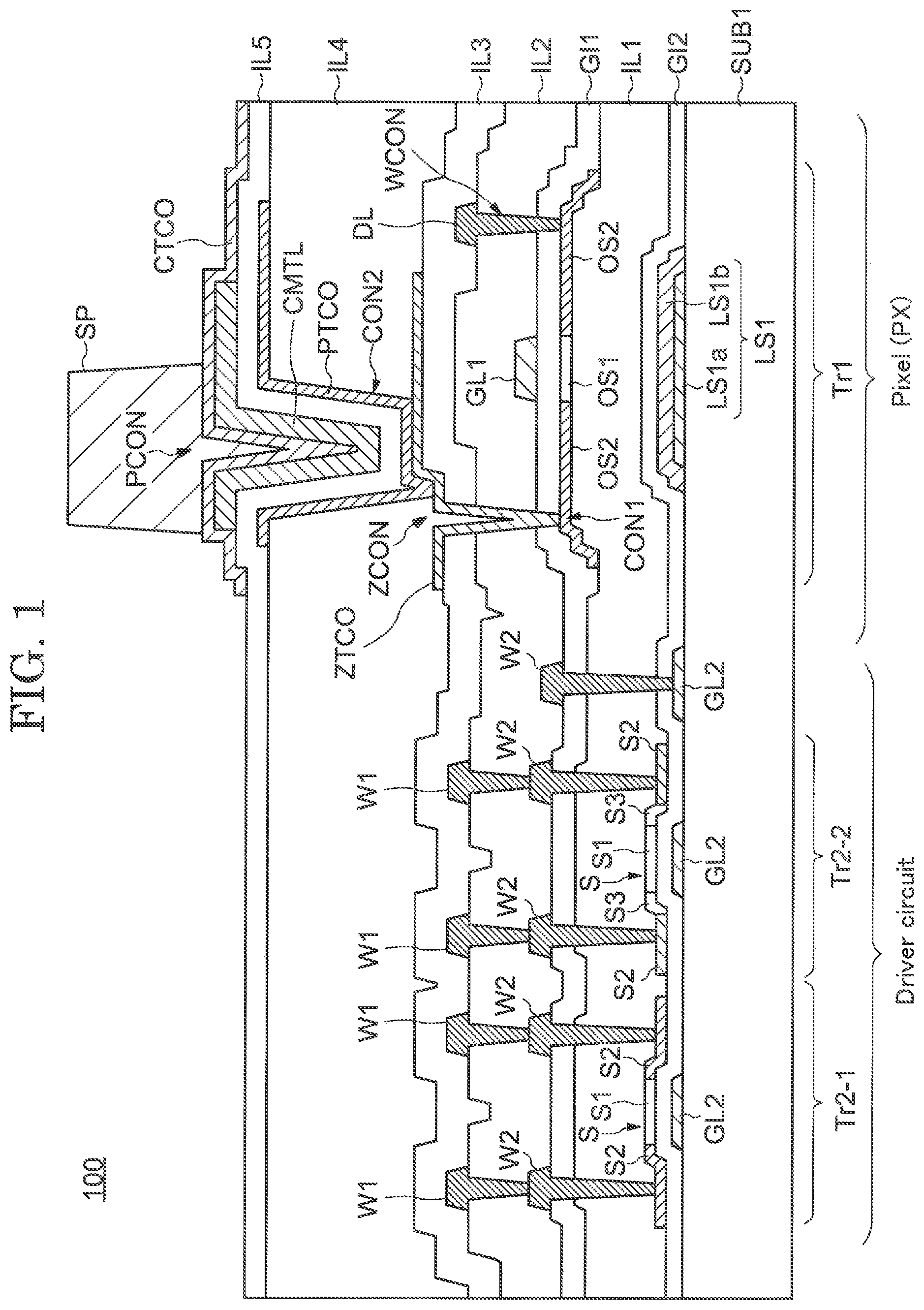
is a cross-sectional view showing an outline of each layer arranged on a first substrate SUB 1 constituting a display device 100 according to an embodiment of the present invention. As shown in , the first substrate SUB 1 is arranged with a first transistor Tr 1 , a second transistor Tr 2 , a data signal line DL, a first wiring W 1 , a second wiring W 2 , a connection electrode ZTCO, a pixel electrode PTCO, a common auxiliary electrode CMTL, and a common electrode CTCO. Although the symbol TCO has no particular meaning, it may be used herein to refer to a transparent conductive oxide such as ITO, ZnO, IZO, or the like. The first transistor Tr 1 is an element included in the pixel PX of the display device 100 , and the second transistor Tr 2 is an element included in the driver circuit. Although the details will be described later, the driver circuit is a circuit for driving the pixel PX.
1.1 First Transistor
The first transistor Tr 1 includes a semiconductor layer OS, a gate insulating layer GI 1 , and a gate electrode GL 1 . The semiconductor layer OS is, for example, an oxide semiconductor layer. The semiconductor layer OS may be a polycrystalline silicon layer. The gate electrode GL 1 faces the semiconductor layer OS. The gate insulating layer GI 1 is arranged between the semiconductor layer OS and the gate electrode GL 1 . Although shows an example of a top gate transistor in which the semiconductor layer OS is arranged on the substrate SUB side of the gate electrode GL 1 , a bottom gate transistor in which the positional relationship between the gate electrode GL 1 and the semiconductor layer OS is reversed may be used.
The semiconductor layer OS includes a first semiconductor region OS 1 and a second semiconductor region OS 2 . The first semiconductor region OS 1 is a region where the semiconductor layer OS overlaps the gate electrode GL 1 , and corresponds to a region called a channel in the first transistor Tr 1 . A conductive state and a non-conductive state of the first transistor Tr 1 are controlled according to a gate voltage applied to the gate electrode GL 1 . The second semiconductor region OS 2 corresponds to a source region and a drain region. The second semiconductor region OS 2 is continuous from the first semiconductor region OS 1 , and is also a region having electrical conductivity higher than that of the first semiconductor region OS 1 .
A second insulating layer IL 2 is arranged on the gate electrode GL 1 . The data signal line DL is arranged on the second insulating layer IL 2 . The data signal line DL is connected to the second semiconductor region OS 2 via an opening WCON arranged in the second insulating layer IL 2 and the gate insulating layer GI 1 . The data signal line DL is a wire for transmitting a data signal related to the gradation of an image. A third insulating layer IL 3 is arranged on the second insulating layer IL 2 and the data signal line DL. The connection electrode ZTCO is arranged on the third insulating layer IL 3 . The connection electrode ZTCO is connected to the second semiconductor region OS 2 via an opening ZCON arranged in the third insulating layer IL 3 , the second insulating layer IL 2 , and the gate insulating layer GI 1 . The connection electrode ZTCO is in contact with the second semiconductor region OS 2 at the bottom of the opening ZCON. The connection electrode ZTCO is formed of a transparent conductive film.
A region where the connection electrode ZTCO and the second semiconductor region OS 2 contact each other is referred to as a first contact region CON 1 . The connection electrode ZTCO is connected to the second semiconductor region OS 2 in the first contact region CON 1 arranged at a position which does not overlap the gate electrode GL 1 and the data signal line DL in a plan view.
A fourth insulating layer IL 4 is arranged on the connection electrode ZTCO. The fourth insulating layer IL 4 is an insulating layer, also called a planarizing layer, and relaxes unevenness formed by the semiconductor layer OS, the gate electrode GL 1 , and the like arranged below the fourth insulating layer IL 4 . The pixel electrode PTCO is arranged on the fourth insulating layer IL 4 . The pixel electrode PTCO is connected to the connection electrode ZTCO via an opening PCON arranged in the fourth insulating layer IL 4 . A region where the connection electrode ZTCO and the pixel electrode PTCO contact each other is referred to as a second contact region CON 2 . The second contact region CON 2 overlaps the gate electrode GL 1 in a plan view. The pixel electrode PTCO is formed of a transparent conductive film.
A fifth insulating layer IL 5 is arranged on the pixel electrode PTCO. The common auxiliary electrode CMTL and the common electrode CTCO are arranged on the fifth insulating layer IL 5 . The common auxiliary electrode CMTL and the common electrode CTCO have different planar patterns. The common auxiliary electrode CMTL is a metal layer. The common electrode CTCO is a transparent conductive layer. The electrical resistance of the common auxiliary electrode CMTL is lower than that of the common electrode CTCO. The common auxiliary electrode CMTL also functions as a light shielding layer, and for example, it is possible to suppress the occurrence of color mixing by shielding light from adjacent pixels. A plurality of first spacers SP 1 are arranged on the common electrode CTCO.
The plurality of first spacers SP 1 are arranged with a certain distance therebetween on the first substrate SUB 1 . The plurality of first spacers SP 1 are not arranged corresponding to all the pixels, but are arranged in an area between a part of the pixels and pixels adjacent thereto. A height of each of the plurality of first spacers SP 1 is half of a cell gap. A plurality of second spacers is also arranged on the second substrate SUB 2 . The plurality of second spacers of the second substrate SUB 2 and the plurality of first spacers SP 1 of the first substrate SUB 1 are arranged to overlap each other in a plan view.
A first light shielding layer LS 1 is arranged on the first substrate SUB 1 . The first light shielding layer LS 1 is arranged in the region of the pixel PX. shows the first light shielding layers LS 1 a , LS 1 b as the first light shielding layer LS 1 . The first light shielding layer LS 1 may be composed of only the first light shielding layer LS 1 a or only the first light shielding layer LS 1 b . The first light shielding layer LS 1 is arranged in a region where at least the gate electrode GL 1 and the semiconductor layer OS overlap each other in a plan view. In other words, the first light shielding layer LS 1 is arranged in a region overlapping the semiconductor layer OS in a plan view. The first light shielding layer LS 1 prevents light incident from the side of the first substrate SUB 1 from reaching the first semiconductor region OS 1 . The first light shielding layer LS 1 defines an aperture range of the pixel PX. A voltage may be applied to the first light shielding layer LS 1 when the first light shielding layer LS 1 is formed of a conductive film. The first light shielding layer LS 1 and the gate electrode GL 1 may be electrically connected when a voltage is applied to the first light shielding layer LS 1 . The first contact region CON 1 is arranged in a region which does not overlap the first light shielding layer LS 1 in a plan view.
1-2. Second Transistor
The driver circuit includes the second transistors Tr 2 (p-channel transistor Tr 2 - 1 and n-channel transistor Tr 2 - 2 ). Each of the p-channel transistor Tr 2 - 1 and the n-channel transistor Tr 2 - 2 includes a gate electrode GL 2 , a gate insulating layer GI 2 , and a semiconductor layer S. The semiconductor layer S includes a first semiconductor region S 1 , a second semiconductor region S 2 , and a third semiconductor region S 3 . The first semiconductor region S 1 of the semiconductor layer S corresponds to a region for forming a channel, the second semiconductor region S 2 corresponds to a region for forming a source region and a drain region, and the third semiconductor region S 3 corresponds to a region for forming a lightly doped drain (LDD). The gate electrode GL 2 includes a region overlapping the first semiconductor region S 1 . The gate insulating layer GI 2 is arranged between the semiconductor layer S and the gate electrode GL 2 . shows a bottom gate transistor in which the gate electrode GL 2 is arranged on the first substrate SUB 1 side of the semiconductor layer S in the second transistors Tr 2 (p-channel transistor Tr 2 - 1 and n-channel transistor Tr 2 - 2 ). The second transistors Tr 2 (p-channel transistor Tr 2 - 1 and n-channel transistor Tr 2 - 2 ), however, may be a top-gate transistor in which the positional relationship between the semiconductor layer S and the gate electrode GL 2 is reversed.
The p-channel transistor Tr 2 - 1 includes the first semiconductor region S 1 and the second semiconductor region S 2 . The n-channel transistor Tr 2 - 2 includes the first semiconductor region S 1 , the second semiconductor region S 2 , and the third semiconductor region S 3 . The first semiconductor region S 1 overlaps the gate electrode GL 2 in a plan view, and functions as a channel of the p-channel transistor Tr 2 - 1 and the n-channel transistor Tr 2 - 2 , and the second semiconductor region S 2 functions as a source region and a drain region. The third semiconductor region S 3 of the n-channel transistor Tr 2 - 2 has a higher resistance than that of the second semiconductor region S 2 and is also called a lightly doped drain (LDD), and has a function of preventing hot carrier degradation.
The first insulating layer IL 1 and the gate insulating layer GI 1 are arranged on the semiconductor layer S. The gate insulating layer GI 1 functions as an interlayer film for the p-channel transistor Tr 2 - 1 and the n-channel transistor Tr 2 - 2 . The second wiring W 2 is arranged on these insulating layers. The second wiring W 2 is connected to the second semiconductor region S 2 via openings arranged in the first insulating layer IL 1 and the gate insulating layer GI 1 . The second insulating layer IL 2 is arranged on the second wiring W 2 . The first wiring W 1 is arranged on the second insulating layer IL 2 . The first wiring W 1 is connected to the second wiring W 2 through an opening arranged in the second insulating layer IL 2 .
The gate electrode GL 2 and the first light shielding layer LS 1 a are the same layer. The second wiring W 2 and the gate electrode GL 1 are the same layer. Here, the same layer means that a plurality of members is simultaneously formed by patterning one layer (formed by the same etching process).
2. Partial Cross-Sectional Structure of the Pixel
shows an example of a partial cross-sectional structure of the pixel PX. The pixel PX includes the first substrate SUB 1 , the second substrate SUB 2 , and the liquid crystal layer LC between the first substrate SUB 1 and the second substrate SUB 2 . As described with reference to , the first substrate SUB 1 includes the first light shielding layer LS 1 , the first transistor Tr 1 , the connection electrode ZTCO, the pixel electrode PTCO, and the common electrode CTCO. The second substrate SUB 2 includes the second light shielding layer BM, a color filter layer CF (first color filter layer CF 1 , second color filter layer CF 2 ), and an overcoat layer OC. As described above, the second substrate SUB 2 is arranged with the second spacers SP 2 at the position corresponding to the first spacers SP 1 . The distance (cell gap) between the first substrate SUB 1 and the second substrate SUB 2 is held at a fixed distance by the first spacers SP 1 and the second spacers SP 2 . It should be noted that, in addition to the above configuration, a configuration in which the first spacers SP 1 directly contacts a layer (for example, an orientation film) forming the outermost surface of the second substrate SUB 2 can also be adopted, and a configuration in which the second spacers SP 2 directly contacts a layer forming the outermost surface of the first substrate SUB 1 can also be adopted. Even in such a case, the second contact region CON 2 is filled with the material forming the first spacers SP 1 , and the second contact region CON 2 is planarized.
As shown in , a configuration lower than the liquid crystal layer LC, that is, the first substrate SUB 1 and each configuration laminated on the first substrate SUB 1 may be referred to as an array substrate. Similarly, the structure of the layer above the liquid crystal layer LC, that is, the second substrate SUB 2 and the structures laminated on the second substrate SUB 2 may be referred to as a counter substrate.
The second light shielding layer BM is formed of an organic resin material containing, for example, a black pigment. The second light shielding layer BM is arranged in the boundary region of the pixel PX. The second light shielding layer BM is arranged in a boundary region between the first color filter layer CF 1 and the second color filter layer CF 2 . The first color filter layer CF 1 and the second color filter layer CF 2 are colored in a predetermined color and have translucency, and are colored in different hues. The overcoat layer OC is arranged on the color filter layer CF. The liquid crystal layer LC is arranged between the first substrate SUB 1 (array substrate) and the second substrate SUB 2 (counter substrate). In other words, the liquid crystal layer LC is arranged between the first light shielding layer LS 1 and the second light shielding layer BM. Note that shows an alignment film for defining an initial alignment state of the liquid crystal layer LC, which is omitted.
3. Planar Layout of Pixels
The display device 100 has a pixel part 102 in which the plurality of pixels PX including the elements shown in are arranged. shows a planar schematic structure of the pixel part 102 when viewed from the second substrate SUB 2 side. shows an embodiment in which the pixel PX includes a first sub-pixel SPX 1 , a second sub-pixel SPX 2 , and a third sub-pixel SPX 3 . For example, the first sub-pixel SPX 1 is a sub-pixel corresponding to blue color, the second sub-pixel SPX 2 is a sub-pixel corresponding to green color, and the third sub-pixel SPX 3 is a sub-pixel corresponding to red color. Colors in sub-pixels can be changed, for example, the first sub-pixel SPX 1 may have red and the third sub-pixel SPX 3 may have blue.
shows that the first sub-pixel SPX 1 , the second sub-pixel SPX 2 , and the third sub-pixel SPX 3 are arranged in the first direction D 1 . The pixels PX including the sub-pixels having the same configuration as the first sub-pixel SPX 1 , the second sub-pixel SPX 2 , and the third sub-pixel PX 3 are arranged in a first direction D 1 and a second direction D 2 intersecting the first direction D 1 .
The first sub-pixel SPX 1 includes a first semiconductor layer OSa, a first connection electrode ZTCO 1 , and a first pixel electrode PTCO 1 , the second sub-pixel SPX 2 includes a second semiconductor layer OSb, a second connection electrode ZTCO 2 , and a second pixel electrode PTCO 2 , and the third sub-pixel SPX 3 includes a third semiconductor layer OSc, a third connection electrode ZTCO 3 , and a third pixel electrode PTCO 3 . The first pixel electrode PTCO 1 , the second pixel electrode PTCO 2 , and the third pixel electrode PTCO 3 are surrounded by the first light shielding layers LS 1 , LS 2 , and the second light shielding layer BM in a plan view, respectively, and a region (a region surrounded by the light shielding layer) exposed from these light shielding layers in a plan view becomes a light transmitting region. The first sub-pixel SPX 1 , the second sub-pixel SPX 2 , and the third sub-pixel SPX 3 are defined with apertures (translucent regions) by the first light shielding layers LS 1 , LS 2 and the second light shielding layer BM.
The scanning signal lines SCL extending in the first direction D 1 and the data signal lines DL (the first data signal line DL 1 , the second data signal line DL 2 , and the third data signal line DL 3 ) extending in the second direction D 2 are arranged in the pixel part 102 . One of the scanning signal lines SCL is arranged to intersect with the first semiconductor layer OSa, the second semiconductor layer OSb, and the third semiconductor layer OSc, and the intersecting part functions as a gate electrode (GL 1 ). The scanning signal lines SCL and the data signal lines DL (first data signal line DL 1 , second data signal line DL 2 , and third data signal line DL 3 ) shown in are arranged between the first light shielding layer LS 1 and the second light shielding layer BM in cross sectional views, as is apparent when compared with .
The first light shielding layer LS 1 has a pattern extending in the first direction D 1 . The first light shielding layer LS 1 is arranged at a position overlapping the scanning signal lines SCL extending in the first direction D 1 . A width of the scanning signal line SCL is smaller than a width of the first light shielding layer LS 1 . The scanning signal lines SCL is arranged in a region inside the pattern of the first light shielding layer LS 1 . The light shielding layer LS 1 is arranged to intersect with the first semiconductor layer OSa, the second semiconductor layer OSb, and the third semiconductor layer OSc. The first light shielding layers LS 1 , LS 2 may have a two-layer structure that may include the first light shielding layer LS 1 a as a lower layer and the first light shielding layer LS 1 b as a upper layer. A width of the first light shielding layer LS 1 b is wider than a width of the first light shielding layer LS 1 a . The first light shielding layer LS 1 a and the second light shielding layer LS 1 b are each formed of a metal film, and a width of the upper first light shielding layer LSb is larger than a width of the first light shielding layer LSa. In other words, it is preferable that the first light shielding layer LS 1 has a structure in which at least two metal films are laminated, and the width of the upper metal layer is larger than the width of the lower metal layer. Both end parts defining the width of the first light shielding layer LS 1 overlap with the first pixel electrodes PTCO 1 , the second pixel electrodes PTCO 2 , and the third pixel electrodes PTCO 3 arranged along the first direction D 1 . The first light shielding layer LS 2 adjacent to the first light shielding layer LS 1 has the same pattern of the first light shielding layer LS 1 ( shows a part thereof) and is arranged so that an end part in the width direction overlaps the first pixel electrodes PTCO 1 , the second pixel electrodes PTCO 2 , and the third pixel electrodes PTCO 3 . In other words, the first pixel electrodes PTCO 1 , the second pixel electrodes PTCO 2 , and the third pixel electrodes PTCO 3 are arranged so that both ends along the first direction D 1 overlap the first light shielding layers LS 1 , LS 2 .
The second light shielding layer BM includes a pattern extending in the second direction D 2 . The second light shielding layer BM has a shape overlapping the first data signal line DL 1 , the second data signal line DL 2 , and the third data signal line DL 3 extending in the second direction D 2 in a plan view. The second light shielding layer BM is arranged so that parts along the second direction D 2 overlaps one end of the first semiconductor layer OSa, the second semiconductor layer OSb, and the third semiconductor layer OSc. Further, the second light shielding layer BM may include a pattern extending in the first direction D 1 and overlapping the scanning signal lines SCL. The pattern extending in the first direction D 1 is a continuous pattern with the pattern extending in the second direction D 2 , and is connected to the patterns extending in the adjacent second direction D 2 . Part of the second light shielding layer BM extending in the first direction D 1 (pattern extending in the first direction D 1 ) overlaps the scanning signal lines SCL and the first light shielding layers LS 1 , LS 2 , and has a width narrower than the first light shielding layers LS 1 , LS 2 . The second light shielding layer BM is arranged to overlap both sides along the second direction D 2 of the first pixel electrodes PTCO 1 , the second pixel electrodes PTCO 2 , and the third pixel electrodes PTCO 3 .
As described above, the first pixel electrodes PTCO 1 , the second pixel electrodes PTCO 2 , and the third pixel electrodes PTCO 3 are surrounded while partially overlapping the first light shielding layers LS 1 , LS 2 , and the second light shielding layer BM in a plan view. Here, an area of a region where the first light shielding layers LS 1 , LS 2 overlap one of the first pixel electrodes PTCO 1 is different from an area of a region where the first light shielding layers LS 1 , LS 2 overlap one of the second pixel electrodes PTCO 2 and one of the third pixel electrodes PTCO 3 . Specifically, the area where the first light shielding layers LS 1 , LS 2 overlap the one of first pixel electrodes PTCO 1 is larger than the area where the first light shielding layers LS 1 , LS 2 overlap one of the second pixel electrodes PTCO 2 and one of the third pixel electrodes PTCO 3 . The area where the first light shielding layers LS 1 , LS 2 overlap one of the second pixel electrodes PTCO 2 is smaller than the area where the first light shielding layers LS 1 , LS 2 overlap one of the first pixel electrodes PTCO 1 and larger than the area where the first light shielding layers LS 1 , LS 2 overlap one of the third pixel electrodes PTCO 3 . The area where the first light shielding layers LS 1 , LS 2 overlap one of the third pixel electrodes PTCO 3 is smaller than the area where the first light shielding layers LS 1 , LS 2 overlap one of the first pixel electrodes PTCO 1 and one of the second pixel electrodes PTCO 2 .
is an enlarged view of the first sub-pixel SPX 1 , the second sub-pixel SPX 2 , and the third sub-pixel SPX 3 . The first pixel electrode PTCO 1 , the second pixel electrode PTCO 2 , and the third pixel electrode PTCO 3 partially overlapped and surrounded by the first light shielding layers LS 1 , LS 2 , and the second light shielding layer BM in a plan view. The first sub-pixel SPX 1 has a first aperture OP 1 exposed from the first light shielding layers LS 1 , LS 2 , the second sub-pixel SPX 2 has a second aperture OP 2 , and the third sub-pixel SPX 3 has a third aperture OP 3 .
The sizes (areas) of the first aperture OP 1 , the second aperture OP 2 , and the third aperture OP 3 are different because the widths of the first light shielding layers LS 1 , LS 2 are different for each aperture. That is, while the width X 1 of the first sub-pixel SPX 1 , the second sub-pixel SPX 2 , and the third sub-pixel SPX 3 in the first direction D 1 is the same for the three pixels, the width in the second direction D 2 has the relationship Y 1 <Y 2 <Y 3 when the first sub-pixel SPX 1 has the length Y 1 , the second sub-pixel SPX 2 has the length Y 2 , and the third sub-pixel SPX 3 has the length Y 3 . The difference in the length in the second direction D 2 in each sub-pixel is based on the difference in the widths (or the length in the second direction D 2 ) of the first light shielding layers LS 1 , LS 2 . The first light shielding layers LS 1 , LS 2 have a part corresponding to the first sub-pixel SPX 1 having a large width, a part corresponding to the third sub-pixel SPX 3 having a small width, and a part corresponding to the second sub-pixel SPX 2 having an intermediate width.
In this way, the width of one or both of the first light shielding layers LS 1 , LS 2 sandwiching the first sub-pixel SPX 1 , the second sub-pixel SPX 2 , and the third sub-pixel SPX 3 varies along the first direction D 1 , so that the area of the aperture of each pixel can be made different. That is, it is possible to make the aperture ratios of the first sub-pixel SPX 1 , the second sub-pixel SPX 2 , and the third sub-pixel SPX 3 different by adjusting the widths of the first light shielding layer LS 1 and the first light shielding layer LS 2 . Although this embodiment shows an example in which the widths of the first light shielding layers LS 1 , LS 2 are different, the widths of the second light shielding layer BM may also be different at the same time. The aperture ratio refers to the ratio of the area not shielded by the light shielding layer to the area occupied by one pixel (or sub-pixel). The area of each pixel PX (or sub-pixel SPX) is determined, for example, according to the distance between the centers of adjacent scanning signal lines SCL and adjacent data signal lines DL, and has a size common to each sub-pixel regardless of color.
When the first sub-pixel SPX 1 is a pixel corresponding to blue, the second sub-pixel SPX 2 is a sub-pixel corresponding to green, and the third sub-pixel SPX 3 is a sub-pixel corresponding to red, it is possible to increase the aperture ratio (or the area of the aperture) of the sub-pixel corresponding to red by the first light shielding layer LS 1 in comparison with the aperture ratio (or the area of the aperture) of the sub-pixel corresponding to blue and the sub-pixel corresponding to green.
The pattern width of the first light shielding layers LS 1 , LS 2 varies along the first direction D 1 in order to make the size of the overlapping areas with each of the pixel electrodes arranged in the first direction D 1 different.
The first light shielding layer LS 1 is also utilized to shield the region of the spacer SP. shows the pattern of the first light shielding layer LS 1 in the region of the first spacer SP 1 . Although the first light shielding layer LS 1 has a pattern the width of which changes at a certain manner along the first direction D 1 , it also has an irregular pattern in the region of the first spacer SP 1 . That is, the first light shielding layer LS 1 has a pattern wider than other regions in order to shield the region of the first spacer SP 1 .
On the other hand, the second light shielding layer BM does not have an irregular pattern similar to the first light shielding layer SL 1 even in the region where the first spacer SP 1 is arranged, but has the same pattern as the other regions. Although a part of the first spacer SP 1 is exposed from the second light shielding layer BM, since the first light shielding layer LS 1 shields the first spacer SP 1 from light, there is no influence on the display of the image. Since the second light shielding layer BM is formed of a resin material, it is difficult to form a fine and precise pattern. In order to shade the first spacer SP 1 with the second shading layer BM, it is necessary to design a wide area of the shading part in consideration of the margin. On the other hand, according to the present embodiment, since the first light shielding layer LS 1 has a fine pattern, the first spacer SP 1 can be reliably shielded from light, and the aperture ratio of the pixel can be prevented from becoming smaller more than necessary. Therefore, according to the present embodiment, as shown in , a part of the first spacer SP 1 is not shielded by the second light shielding layer BM when the relationship between the second light shielding layer BM and the first spacer SP 1 is viewed. That is, the first spacer SP 1 (or the whole of the spacer, which is formed by the first spacer SP 1 and the second spacer SP 2 in the present embodiment) has a lower bottom surface on the first substrate SUB 1 side overlapping the entire first light shielding layer LS 1 arranged on the first substrate SUB 1 , while an upper bottom surface on the second substrate SUB 2 side is partially exposed from the second light shielding layer BM arranged on the second substrate SUB 2 . As shown in , the first spacer SP 1 is not only arranged on the second contact region CON 2 of a predetermined pixel, but also overlaps the pixel electrode PTCO over the second contact region CON 2 , the semiconductor layer OS connected to the pixel electrode PTCO, and the pixel electrode adjacent to the pixel electrode PTCO in the second direction D 2 . As described above, when a high definition pixel part 102 is formed, the spacer becomes relatively larger than the size of the pixel PX. In this embodiment, the radius of the first spacer SP 1 is larger than the length in the first direction of the pixel PX defined between the centers of the data signal lines DL, and the first spacer SP 1 overlaps any of the pair of adjacent data signal lines DL 2 , DL 3 .
A region where the first pixel electrode PTCO 1 is exposed from the first light shielding layers LS 1 , LS 2 and the second light shielding layer BM constitutes a light transmissive region. This light transmissive region corresponds to the aperture of the first sub-pixel SPX 1 . That is, the aperture ratio of the first sub-pixel SPX 1 is defined by the first light shielding layers LS 1 , LS 2 and the second light shielding layer BM. Similarly, the aperture ratios of the second sub-pixel SPX 2 and the third sub-pixel SPX 3 are also defined by the first light shielding layers LS 1 , LS 2 and the second light shielding layer BM. The aperture ratios of the first sub-pixel SPX 1 , the second sub-pixel SPX 2 , and the third sub-pixel SPX 3 are different. The difference in the aperture ratio of each pixel is defined by the difference in the area where the first light shielding layers LS 1 , LS 2 overlap the pixel electrode.
It should be noted that the first light shielding layers LS 1 , LS 2 are arranged on the first substrate SUB 1 , and the second light shielding layer BM is arranged on the second substrate SUB 2 . As shown in and , the first light shielding layer LS 1 is arranged on a lower layer side than the scanning signal line SCL (and the gate electrode GL 1 ) and the pixel electrode PTCO. The first light shielding layer LS 1 is formed with a metal film on the first substrate SUB 1 , and the above-described pattern is formed by a photolithography process. The first light shielding layer LS 1 is a layer first patterned on the first substrate SUB 1 , and the scanning signal line SCL (and the gate electrode GL 1 ) and the pixel electrode PTCO formed in the subsequent steps are positioned by alignment markers formed in the same layer as the first light shielding layer LS 1 . The first light shielding layer LS 1 is formed by dry etching or wet etching a metal film which is an inorganic material, so that the first light shielding layer LS 1 can be formed in a fine pattern. The pixel electrode PTCO has a transparent conductive film formed on the first substrate SUB 1 formed in a predetermined shape through a photolithography process. The mutual positions of the first light shielding layer LS 1 and the pixel electrode PTCO depend on the alignment accuracy of the photomask in the exposure apparatus and can be aligned with high accuracy. On the other hand, the second light shielding layer BM is formed of an organic resin material containing a black pigment. Although the second light shielding layer BM is not suitable for forming a high-definition pattern such as the first light shielding layer LS 1 , the second light shielding layer BM can be inexpensively manufactured in a region having a large area with a small number of steps.
If the aperture ratio of pixels is to be adjusted only with the second light shielding layer BM formed on the second substrate SUB 2 , a margin must be maintained to account for alignment accuracy (misalignment of lamination) when the first substrate SUB 1 and second substrate SUM 2 are bonded together. The display device 100 according to the present embodiment finely controls the aperture ratio of pixels by combining the above two kinds of light shielding layers. That is, not only the second light shielding layer BM arranged on the second substrate SUB 2 defines the aperture ratio of the pixels, but also the first light shielding layer LS 1 arranged on the first substrate SUB 1 and the second light shielding layer BM arranged on the second substrate SUB 2 are utilized, and the aperture area (at least with respect to the definition in the second direction) is controlled by the first light shielding layer LS 1 to precisely control the aperture ratio of each pixel. Thus, even if the pixel is formed to a high definition (even if the size of the pixel is narrowed), the aperture ratio of the pixel can be precisely controlled.
4. Detailed Layout of Each Layer Constituting the Pixel
A detailed layout of each layer constituting the pixel PX will be described below.
4-1. First Light Shielding Layer
shows the first light shielding layers LS 1 , LS 2 , LS 3 . The first light shielding layers LS 1 , LS 2 , LS 3 have a pattern extending in the first direction D 1 . As described with reference to , the pattern width of the first light shielding layer LS 1 is different according to the arrangement of the pixels. That is, the first light shielding layer LS 1 includes a part having a wider width along the first direction D 1 and a part having a narrower width than the part having a wider width. For example, when the first sub-pixel SPX 1 , the second sub-pixel SPX 2 , and the third sub-pixel SPX 3 as shown in are arranged periodically along the first direction D 1 , the first light shielding layer LS 1 has a pattern that changes periodically. The same is true for the first light shielding layers LS 2 , LS 3 .
As shown in , the first light shielding layer LS 1 may have a two-layer structure comprised of the first light shielding layer LS 1 a and the first light shielding layer LS 1 b . It is possible to enhance the light shielding performance by forming the first light shielding layer LS 1 into a metal film with a two-layer structure.
4-2. Semiconductor Layer
As shown in , the first semiconductor layer OSa, the second semiconductor layer OSb, and the third semiconductor layer OSc have island patterns extending in the second direction D 2 . The first semiconductor layer OSa, the second semiconductor layer OSb, and the third semiconductor layer OSc are arranged on the upper layer side of the first light shielding layer LS 1 . The first semiconductor layer OSa, the second semiconductor layer OSb, and the third semiconductor layer OSc are arranged so that they partially overlap the first light shielding layer LS 1 .
4-3. Scanning Signal Line
shows the scanning signal line SCL. The scanning signal line SCL extends in the first direction D 1 to intersect with the first semiconductor layer OSa, the second semiconductor layer OSb, and the third semiconductor layer OSc. A part where the scanning signal line SCL intersects the first semiconductor layer OSa, the second semiconductor layer OSb, and the third semiconductor layer OSc functions as a gate electrode (GL 1 ). The pattern of the scanning signal line SCL (gate electrode GL 1 ) is arranged inside the pattern of the first light shielding layer LS 1 .
4-4. Data Signal Line
shows the first data signal line DL 1 , the second data signal line DL 2 , and the third data signal line DL 3 . The first data signal line DL 1 , the second data signal line DL 2 , and the third data signal line DL 3 extend in the second direction D 2 and are arranged to intersect the scanning signal line SCL. As shown in , the aperture WCON is arranged in a region overlapping the first data signal line DL 1 , the second data signal line DL 2 , and the third data signal line DL 3 near one end of the island pattern of the first semiconductor layer OSa, the second semiconductor layer OSb, and the third semiconductor layer OSc. A main part of the first semiconductor layer OSa is arranged between the first data signal line DL 1 and the second data signal line DL 2 and extends in the second direction D 2 . One end of the first semiconductor layer OSa has a pattern bent toward the opening WCON from a part sandwiched between the first data signal line DL 1 and the second data signal line DL 2 . The first data signal line DL 1 is arranged to overlap the opening WCON. The first semiconductor layer OSa is connected to the first data signal line DL 1 at the opening WCON. The same is true for the second semiconductor layer OSb and the third semiconductor layer OSc.
4-5. Connection Electrode
As shown in , the opening ZCON is arranged to overlap the island pattern of the first semiconductor layer OSa, the second semiconductor layer OSb, and the third semiconductor layer OSc. While the opening WCON is arranged on one end side of the first semiconductor layer OSa, the second semiconductor layer OSb, and the third semiconductor layer OSc, the opening ZCON is arranged on the other end side of the first semiconductor layer OSa, the second semiconductor layer OSb, and the third semiconductor layer OSc. The first light shielding layer LS 1 or the scanning signal line SCL passes between one end and the other end of the first semiconductor layer OSa, the second semiconductor layer OSb, and the third semiconductor layer OSc. The opening ZCON is arranged at a position not overlapping the scanning signal line SCL.
The connection electrode ZTCO is arranged between the first data signal line DL 1 and the second data signal line DL 2 to overlap the first semiconductor layer OSa. The connection electrode ZTCO is connected to the first semiconductor layer OSa at the opening ZCON (first contact region CON 1 ). The second semiconductor layer OSb and the third semiconductor layer OSc are similarly connected to the connection electrode ZTCO. The connection electrode ZTCO has a pattern extending along the second direction D 2 and is arranged to extend from a part where the opening ZCON is formed to a region exceeding the scanning signal line SCL.
4-6. Pixel Electrode
shows the first pixel electrode PTCO 1 , the second pixel electrode PTCO 2 , and the third pixel electrode PTCO 3 . The first pixel electrode PTCO 1 is connected to the first connection electrode ZTCO 1 through the opening PCON, the second pixel electrode PTCO 2 is connected to the second connection electrode ZTCO 2 through the opening PCON, and the third pixel electrode PTCO 3 is connected to the third connection electrode ZTCO 3 through the opening PCON. The opening PCON is arranged in a region near the upper ends of the patterns of the first connection electrode ZTCO 1 , the second connection electrode ZTCO 2 , and the third connection electrode ZTCO 3 and overlaps the pattern of the scanning signal line SCL (gate electrode GL 1 ). The first pixel electrode PTCO 1 is arranged between the first data signal line DL 1 and the second data signal line DL 2 to overlap the scanning signal line SCL (gate electrode GL 1 ), the semiconductor layer OS 1 a , and the first connection electrode ZTC 1 and extend in the second direction D 2 . The same is true for the second pixel electrode PTCO 2 and the third pixel electrode PTCO 3 .
4-7. Common Auxiliary Electrode
shows a common auxiliary electrode CMTL. The common auxiliary electrode CMTL has a lattice-like pattern surrounding the first pixel electrode PTCO 1 , the second pixel electrode PTCO 2 , and the third pixel electrode PTCO 3 . The common auxiliary electrode CMTL includes a vertical pattern extending in the second direction D 2 to overlap the first data signal line DL 1 , the second data signal line DL 2 , and the third data signal line DL 3 , and a horizontal pattern extending in the first direction D 1 to overlap part of the opening PCON. A width of the pattern extending in the first direction D 1 of the common auxiliary electrode CMTL is narrower than the width of the first light shielding layer LS 1 . The common auxiliary electrode CMTL is arranged over the entire pixel part 102 . In other words, the common auxiliary electrode CMTL has a plurality of openings that expose the first pixel electrode PTCO 1 , the second pixel electrode PTCO 2 , and the third pixel electrode PTCO 3 .
The common auxiliary electrode CMTL is formed of a metal film. The common auxiliary electrode CMTL is utilized as an auxiliary electrode for reducing the resistance of the common electrode CTCO, which is formed of a transparent conductive film on the common electrode CMTL and extends over substantially the entire surface of the pixel part 102 .
According to the above configuration, it is possible to define the aperture widths of the first pixel PX 1 , the second pixel PX 2 , and the third pixel PX 3 in the first direction D 1 by adjusting the widths of the common auxiliary electrodes CMTL. That is, it is possible to form a region overlapping the first pixel electrode PTCO 1 , the second pixel electrode PTCO 2 , and the third pixel electrode PTCO 3 by widening the width of the common auxiliary electrode CMTL, and to add a function as a light shielding layer. In other words, the common auxiliary electrode CMTL can replace the function of the second light shielding layer BM arranged on the second substrate SUB 2 .
shows an example in which the aperture of a pixel is defined by the first light shielding layer LS 1 and the second light shielding layer BM, and as shown in , it is also possible to define the aperture size (aperture ratio) of the pixel by the first light shielding layer LS 1 and the common auxiliary electrode CMTL. More specifically, the common auxiliary electrode CMTL is arranged to overlap each data signal line and extend in the second direction, and defines the width of the aperture of each pixel PX in the first direction instead of the second light shielding layer BM. Since the common auxiliary electrode CMTL is patterned by photolithography in the same manner as the first light shielding layer LS 1 , the aperture ratio can be precisely defined even if the pixel PX is reduced in size. According to such a configuration, the second light shielding layer BM on the counter substrate side (second substrate side SUB 2 ) may or may not be arranged. The width of the horizontal pattern of the common auxiliary wiring CMTL in the second direction is equal to the width of the opening PCON, and the width is smaller than the widths of the first light shielding layers LS 1 , LS 2 while covering the opening PCON.
4-8. Common Electrode
shows the common electrode CTCO. The common electrode CTCO is commonly arranged for a plurality of pixels. The common electrode CTCO is provided with slits SL in a region corresponding to the aperture of the first pixel PX 1 , the second pixel PX 2 , and the third pixel PX 3 . The slit SL has a curved shape (a vertically long S-shape), and has a shape in which the width in the extending direction decreases as the tip ends. As described above, the pixel PX driving the liquid crystal in the IPS mode (In-Plane Switching mode) or FFS mode (Fringe Field Switching mode) is provided.
4-9. Material of Each Member Constituting the Pixel
A rigid substrate having translucency and no flexibility such as a glass substrate, a quartz substrate and a sapphire substrate can be used as the first substrate SUB 1 and the second substrate SUB 2 . On the other hand, when the first substrate SUB 1 and the second substrate SUB 2 require flexibility, a flexible substrate containing a resin such as a polyimide substrate, an acrylic substrate, a siloxane substrate, or a fluor resin substrate can be used as the substrate. In order to improve the heat resistance of the first substrate SUB 1 and the second substrate SUB 2 , impurities may be introduced into the resin.
A metal can be used as the scanning signal line SCL (gate electrode GL 1 ), the gate electrode GL 2 , the data signal line DL, the first wiring W 1 , the second wiring W 2 , the first light shielding layer LS 1 , and the common auxiliary electrode CMTL. For example, aluminum (Al), titanium (Ti), chromium (Cr), cobalt (Co), nickel (Ni), molybdenum (Mo), hafnium (Hf), tantalum (Ta), tungsten (W), bismuth (Bi), silver (Ag), and alloys or compounds thereof are used as these members. The material of these members may be used as a single layer or may be used as a laminate.
An insulating material can be used as the gate insulating layers GI 1 , GI 2 , the first insulating layer IL 1 , the second insulating layer IL 2 , the third insulating layer IL 3 , the fourth insulating layer IL 4 , and the fifth insulating layer IL 5 . For example, an inorganic insulating material such as silicon oxide (SiO x ), silicon oxynitride (SiO x N y ), silicon nitride (Si x Ny), aluminum oxide (AlO x ), aluminum oxynitride (AlO x N y ), and aluminum nitride (AlN x ) can be used as the first insulating layer IL 1 , the second insulating layer IL 2 , the third insulating layer IL 3 , and the fifth insulating layer IL 5 . These insulating layers preferably contain few defects. An organic insulating material such as a polyimide resin, an acrylic resin, an epoxy resin, a silicone resin, a fluor resin, or a siloxane resin can be used as the fourth insulating layer IL 4 . An organic insulating material may be used as the gate insulating layers GI 1 , GI 2 , the first insulating layer IL 1 , the second insulating layer IL 2 , the third insulating layer IL 3 , and the fifth insulating layer IL 5 . The material of these members may be used as a single layer or may be used as a laminate.
As an example of the insulating layer, SiO x having a thickness of 100 nm is used as the gate insulating layer GI 1 . SiO x /Si x N y /SiO x having a total thickness of 600 nm to 700 nm is used as the first insulating layer IL 1 . SiO x /Si x N y having a total thickness of 60 nm to 100 nm is used as the gate insulating layer GI 2 . SiO x /Si x N y /SiO x with a total thickness of 300 nm to 500 nm is used as the second insulating layer IL 2 . SiO x (single layer), Si X N Y (single layer), or their laminations having a total thickness of 200 nm to 500 nm are used as the third insulating layer IL 3 . An organic layer having a thickness of 2 μm to 4 μm is used as the fourth insulating layer IL 4 . Si x N y (single layer) having a thickness of 50 nm to 150 nm is used as the fifth insulating layer IL 5 .
A metal oxide (oxide semiconductor) having semiconductor properties can be used as the semiconductor layer OS. The semiconductor layer OS has transparency. For example, oxide semiconductors containing indium (In), gallium (Ga), zinc (Zn), and oxygen (O) can be used. In particular, an oxide semiconductor having a composition ratio of In:Ga:Zn:O=1:1:1:4 can be used. However, the oxide semiconductor containing In, Ga, Zn, and O used in this embodiment is not limited to the above composition, and an oxide semiconductor having a composition different from the above may be used. For example, the ratio of In may be larger than the above in order to improve the mobility. In order to increase the band gap and reduce the influence of light irradiation, the ratio of Ga may be made larger than the above.
The oxide semiconductor containing In, Ga, Zn and O may be doped with other elements. For example, metal elements such as Al and Sn may be added to the oxide semiconductor. In addition to the oxide semiconductors described above, oxide semiconductors including In and Ga (IGO), oxide semiconductors including In and Zn (IZO), oxide semiconductors including In, Sn and Zn (ITZO), and oxide semiconductors including In and W may be used as the semiconductor layer OS. The semiconductor layer OS may be amorphous or crystalline. The semiconductor layer OS may be a mixed phase of amorphous and crystal.
A transparent conductive layer is used as the connection electrode ZTCO, the pixel electrode PTCO (first pixel electrode PTCO 1 , second pixel electrode PTCO 2 , and third pixel electrode PTCO 3 ), and the common electrode CTCO. A mixture of indium oxide and tin oxide (ITO) and a mixture of indium oxide and zinc oxide (IZO) can be used as the transparent conductive layer. Materials other than those described above may be used as the transparent conductive layer.
5. Configuration of the Display Device
shows a configuration of the display device 100 according to an embodiment of the present invention. The display device 100 includes the first substrate SUB 1 , the second substrate SUB 2 , the driver IC 110 , and the flexible printed circuit board 112 . As shown in this embodiment, the pixel PX including the first light shielding layer LS 1 is arranged on the first substrate SUB 1 , and the second light shielding layer BM and the color filter layer CF are arranged on the second substrate SUB 2 . A sealing material (not shown) is arranged between the first substrate SUB 1 and the second substrate SUB 2 . The first substrate SUB 1 and the second substrate SUB 2 are bonded by a sealing material.
The first substrate SUB 1 includes a pixel part 102 in which the plurality of pixels PX are arranged, the scanning signal line driver circuit 104 arranged in an area outside the pixel part 102 , the data signal line selection circuit 106 , and a terminal part 108 forming a connection with the flexible printed circuit board 112 . The driver IC 110 is mounted on the flexible printed circuit board 112 . The pixel PX includes the first sub-pixel SPX 1 , the second sub-pixel SPX 2 , and the third sub-pixel SPX 3 . The scanning signal line SCL is connected to the scanning signal line driver circuit 104 , and the first data signal line DL 1 , the second data signal line DL 2 , and the third data signal line DL 3 are connected to the data signal line selection circuit 106 .
The first transistor Tr 1 shown in is arranged in the first sub-pixel SPX 1 , the second sub-pixel SPX 2 , and the third sub-pixel SPX 3 . The second transistor Tr 2 is utilized in the scanning signal line driver circuit 104 and the data signal line selection circuit 106 . The pixel part 102 is constituted by the first sub-pixel SPX 1 , the second sub-pixel SPX 2 , and the third sub-pixel SPX 3 shown in and .
Each of the embodiments described above as an embodiment of the present invention can be appropriately combined and implemented as long as they do not contradict each other. Further, the addition, deletion, or design change of components as appropriate by those skilled in the art based on each embodiment are also included in the scope of the present invention as long as they are provided with the gist of the present invention.
It is understood that, even if the effect is different from those provided by each of the above-described embodiments, the effect obvious from the description in the specification or easily predicted by persons ordinarily skilled in the art is apparently derived from the present invention.
Figures (14)
Citations
This patent cites (7)
- US5517341
- US20010012076
- US20030234971
- US20180052548
- US20210055603
- USH10-206889
- US20070118001