Method for Fabricating Semiconductor Device
Abstract
A method for fabricating a semiconductor device includes following steps: A patterned mask layer including a plurality of standing walls and a covering part is formed on a surface of a semiconductor substrate, wherein two adjacent standing walls define a first opening exposing a part of the surface, and the covering part blankets the surface. A first patterned photoresist layer is formed to partially cover the covering part. A first etching process is performed to form a first trench in the substrate, passing through the surface and aligning with the first opening. A portion of the patterned mask layer is removed to form a second opening exposing another portion of the surface. A second etching process is performed to form a second trench in the substrate and define an active area on the surface. The depth of the first trench is greater than that of the second trench.
Claims (10)
1. A method for fabricating a semiconductor device, comprising: forming a patterned mask layer including a plurality of standing walls and at least one covering part on a surface of a semiconductor substrate, wherein at least two adjacent ones of the plurality of standing walls define at least one first opening exposing a portion of the surface, and the at least one covering part blankets over the surface; forming a first patterned photoresist layer to at least partially cover the at least one covering part; performing a first etching process, using a combination of the patterned mask layer and the first patterned photoresist layer as an etching mask, to form at least one first trench in the substrate, passing through the surface and aligning with the at least one first opening; removing a portion of the patterned mask layer to form at least one second opening exposing another portion of the surface; performing a second etching process, using a combination of a remaining portion of the patterned mask layer and the first patterned photoresist layer as an etching mask, to form at least one second trench in the semiconductor substrate and define an active area on the surface, wherein the at least one first trench has a depth greater than that of the at least one second trench.
Show 9 dependent claims
2. The method according to claim 1 , wherein forming the first patterned photoresist layer comprises: forming a patterned sacrificial layer having at least one mandrel unit on the surface; forming a blanket layer conformally covering the at least one mandrel unit and a portion of the surface that is not covered by the at least one mandrel unit; removing a portion of the blanket layer to expose a top surface of the at least one mandrel unit, to make a remaining portion of the blanket layer constitutes the plurality of standing walls and the at least one covering part, wherein each of the standing walls is respectively located on at least one side wall of the at least one mandrel unit, and the at least one covering part covers the portion of the surface; and removing the patterned sacrificial layer.
3. The method according to claim 2 , wherein the at least one mandrel unit has a width substantially equal to an opening width of the at least one first trench.
4. The method according to claim 2 , wherein the patterned sacrificial layer comprises amorphous silicon (a-Si); and the blanket layer comprises silicon nitride.
5. The method according to claim 2 , further comprising forming a clapping layer covering the blanket layer, prior to the step of removing a portion of the blanket layer.
6. The method according to claim 5 , wherein the clapping layer is a photoresist coating; and the step of removing a portion of the blanket layer comprises performing an etch-back process on the blanket layer.
7. The method according to claim 5 , wherein the step of removing a portion of the blanket layer comprises performing a planarization process on the clapping layer and the blanket layer and stopping at the top surface of the at least one mandrel unit.
8. The method according to claim 5 , wherein the at least one second trench is defined by a remaining portion of the at least one covering part and at least one of the plurality of standing walls; and the at least one second trench aligns the at least one second opening.
9. The method according to claim 1 , wherein the semiconductor substrate comprises: a semiconductor base layer; and a pad oxide layer formed on the semiconductor base layer.
10. The method according to claim 1 , wherein the at least one covering part form a non-180° angle with one of the plurality of standing walls.
Full Description
Show full text →
This application claims the benefit of People's Republic of China application Serial No. 202110724797.X, filed Jun. 29, 2021, the subject matter of which is incorporated herein by reference.
BACKGROUND
Technical Field
The disclosure relates to a method for fabricating an integrated circuit structure, and more particularly to a method for fabricating a semiconductor device.
Description of Background
A typical integrated circuit (IC) structure needs to maintain a sufficiently wide (generally more than 100 microns) pitch between a low-voltage region and a high-voltage region to make the IC structure withstanding a large voltage drop and maintain its normal performance and electronic properties. However, as the semiconductor devices involved in the IC structure become more and more dense, the critical size of the semiconductor devices becomes smaller and smaller. The current pitch requirement limits the shrinkage in the critical dimension of the IC structure. In order to solve this problem, the prior art has proposed a deep trench isolation structure to isolate different regions of the semiconductor substrate and reduce the critical dimension of the IC structure. But, in addition to the deep trench isolation structure between the low-voltage region and the high-voltage region, there are also a shallow trench isolation (STI) structure configured between the semiconductor devices in each region, which makes the manufacturing process of the IC structure more complicated. How to form these two kinds of trench structures with different depths in a semiconductor substrate with fewer manufacturing process steps to improve the manufacturing process efficiency of the IC structures has become an important subject for those with ordinary knowledge in the art.
Therefore, there is a need of providing an advanced method for fabricating a semiconductor device to obviate the drawbacks encountered from the prior art.
SUMMARY
One aspect of the present disclosure is to provide a method for fabricating a semiconductor device, wherein the method includes steps as follows: A patterned mask layer including a plurality of standing walls and at least one covering part is formed on a surface of a semiconductor substrate, wherein at least two adjacent ones of the plurality of standing walls define a first opening to expose a portion of the surface, and the at least one covering part blankets over the surface. A first patterned photoresist layer is then formed to at least partially cover the at least one covering part. A first etching process is performed to form at least one first trench in the substrate, passing through the surface and aligning with the at least one first opening. A portion of the patterned mask layer is removed to form at least one second opening exposing another portion of the surface. A second etching process is performed to form at least one second trench in the semiconductor substrate and define an active area on the surface, wherein the at least one first trench has a depth greater than that of the at least one second trench.
In accordance with the aforementioned embodiments of the present disclosure, a method for fabricating a semiconductor device is provided. A patterned sacrificial layer having at least one mandrel unit is used to form a patterned mask layer with a three-dimensional (3D) opening structure on the surface of a semiconductor substrate. An etching process using the patterned mask layer as an etching mask is then performed to etch the surface of the semiconductor substrate. Thereinafter, another photoresist photolithography etching process is performed thereon to form two types of self-aligned trench structures with different depths in the semiconductor substrate, and at least one active region can be defined on the surface of the semiconductor substrate for subsequently forming semiconductor units thereon. Thereby, the processing steps and complexity for forming the semiconductor device can be greatly reduced, and the yield and efficiency for manufacturing the same can be significantly improved.
BRIEF DESCRIPTION OF THE DRAWINGS
The above objects and advantages of the present disclosure will become more readily apparent to those ordinarily skilled in the art after reviewing the following detailed description and accompanying drawings, in which:
is a processing flowchart illustrating a method for fabricating a semiconductor device, in accordance with one embodiment of the present disclosure; and
A to 2 L are cross-sectional views illustrating a series of processing structures for fabricating the semiconductor device according to the method as described in .
DETAILED DESCRIPTION
The embodiments as illustrated below provide a method for fabricating a semiconductor device to improve the processing yield and efficiency for manufacturing the semiconductor device. The present disclosure will now be described more specifically with reference to the following embodiments illustrating the structure and arrangements thereof.
It is to be noted that the following descriptions of preferred embodiments of this disclosure are presented herein for purpose of illustration and description only. It is not intended to be exhaustive or to be limited to the precise form disclosed. Also, it is important to point out that there may be other features, elements, steps, and parameters for implementing the embodiments of the present disclosure which are not specifically illustrated. Thus, the descriptions and the drawings are to be regard as an illustrative sense rather than a restrictive sense. Various modifications and similar arrangements may be provided by the persons skilled in the art within the spirit and scope of the present disclosure. In addition, the illustrations may not be necessarily drawn to scale, and the identical elements of the embodiments are designated with the same reference numerals.
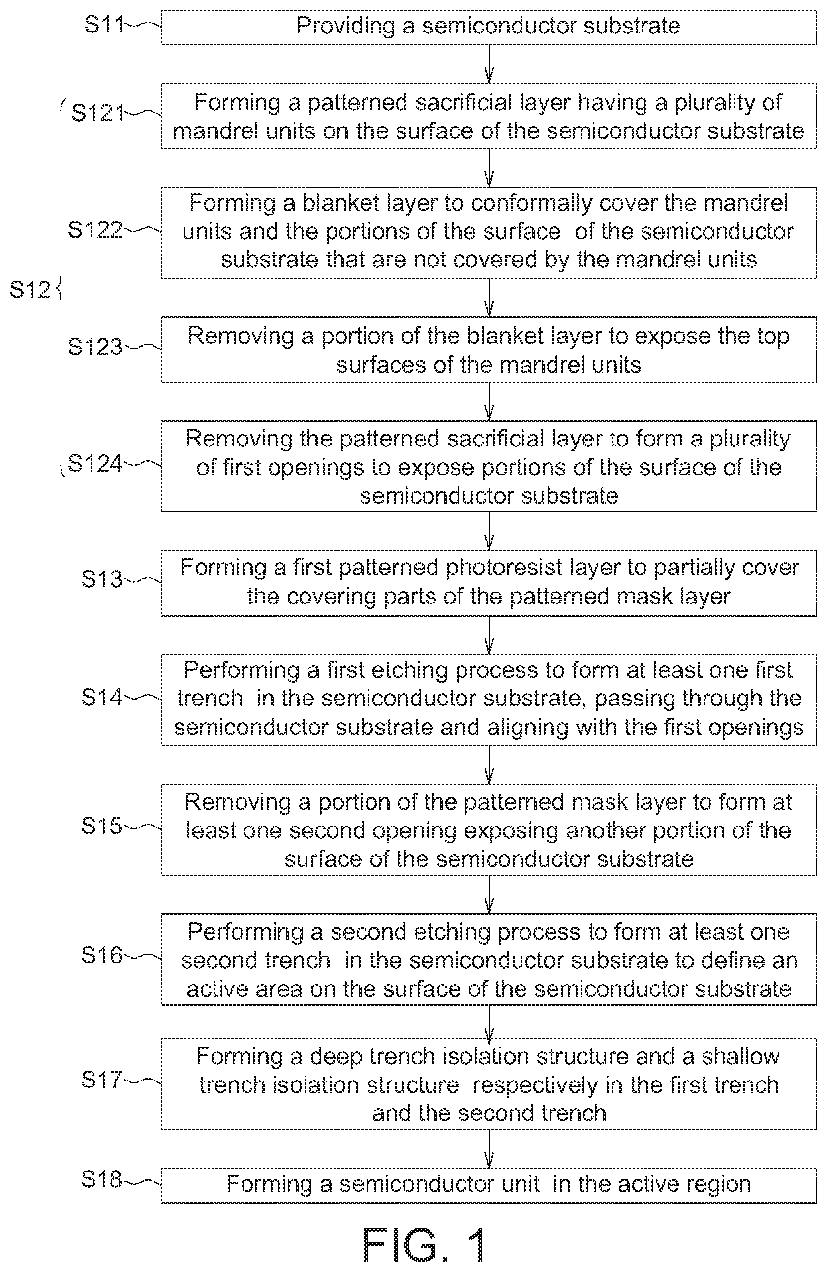
is a processing flowchart illustrating a method for fabricating a semiconductor device 100 , in accordance with one embodiment of the present disclosure; and A to 2 L are cross-sectional views illustrating a series of processing structures for fabricating the semiconductor device 100 according to the method as described in .
The method for fabricating a semiconductor device 100 includes steps as follows: First, referring to step S 11 : a semiconductor substrate 101 is provided. In some embodiments of the present disclosure, the semiconductor substrate 101 may be made of a semiconductor material (such as, silicon (Si) or germanium (Germanium, Ge)) or made of a compound semiconductor material (such as, gallium arsenide (GaAs)). However, in other embodiments, the semiconductor substrate 101 may be a silicon-on-insulator (SOI) substrate. In another embodiment of the present disclosure, the semiconductor substrate 101 is preferably a silicon wafer. In the present embodiment, the semiconductor substrate 101 includes a semiconductor base layer 101 a (for example, a silicon base layer) and a pad oxide layer 101 b formed on the semiconductor base layer 101 a (see A ).
Next, referring to step S 12 : A patterned mask layer 102 is formed on a surface 101 s of the semiconductor substrate 101 , wherein the patterned mask layer 102 includes a plurality of standing walls 102 a and a plurality of covering parts 102 b . In some embodiments, at least two adjacent ones of the plurality of standing walls 102 a define a first opening 103 to expose a portion of the surface 101 s of the semiconductor substrate 101 . Each of the covering parts 102 b of the patterned mask layer 102 blankets over the 101 s of the semiconductor substrate 101 , and forms a non-180° angle θ (for example, a 90° angle) with the standing walls 102 a connected thereto.
The forming of the patterned mask layer 102 includes steps as follows: Firstly, referring to step S 121 : a patterned sacrificial layer 104 having a plurality of mandrel units 104 a is formed on the surface 101 s of the semiconductor substrate 101 (see B ). In the present embodiment, the patterned sacrificial layer 104 is formed by a deposition process, such as physical vapor deposition (PVD) process, a chemical vapor deposition (CVD) process, a sputtering process, or other suitable manufacturing processes. An amorphous silicon (a-Si) layer is formed on the surface 101 s of the substrate; then a portion of the amorphous silicon layer is removed by a dry etching process, such as a reactive ion etching (RIE) process to remain a plurality of three-dimensional amorphous silicon bumps on the surface 101 s of the semiconductor substrate serving as a plurality of mandrel units 104 a . Wherein, each of the mandrel units 104 a has a substantially flat top surface 104 t , and has a vertical cross-section of a wedge-shaped, rectangular, regular or irregular polygon.
Then, referring to step S 122 , a blanket layer 105 is formed to conformally cover these mandrel units 104 a and the portions of the surface 101 s of the semiconductor substrate that are not covered by the mandrel units 104 a (see C ). In some embodiments of the present disclosure, the blanket layer 105 may include silicon nitride. In the present embodiment, since the thickness of the blanket layer 105 is less than the height of the mandrel units 104 a , thus it cannot fill the gaps G between two adjacent ones of the mandrel units 104 a.
Thereafter, referring to step S 123 : a portion of the blanket layer 105 is removed to expose the top surfaces 104 t of the mandrel units 104 a . In some embodiments of the present disclosure, a clapping layer 106 can be firstly formed on the blanket layer 105 to cover the blanket layer 105 and completely fill the gaps G between two adjacent ones of the plurality of mandrel units 104 a , prior to the step of removing a portion of the blanket layer 105 (see D ). In the present embodiment, the clapping layer 106 can be a photoresist coating.
The step of removing a portion of the blanket layer 105 may include performing an etch-back process on the blanket layer 105 (the clapping layer 106 ), removing the portion of the blanket layer 105 disposed on the top surfaces 104 t of the mandrel units 104 a , so as to exposed the top surfaces 104 t of the mandrel units 104 a (see E ).
However, the step of removing the portion of the blanket layer 105 may not be limited to this regard. In some other embodiments of the present disclosure, the step of removing the portion of the blanket layer 105 may include performing a planarization process, such as a chemical mechanical polishing (CMP) process, on the clapping layer 106 and the blanket layer 105 and stopping at the top surfaces 104 t of the mandrel units 104 a.
After removing the remaining clapping layer 106 , the remaining portion of the blanket layer 105 constitutes the plurality of standing walls 102 a and the plurality of covering parts 102 b of the patterned mask layer 102 . Wherein, each of the standing walls 102 a of the patterned mask layer 102 is respectively located on at least one side wall 104 s of the mandrel units 104 a . The covering parts 102 b of the patterned mask layer 102 cover the portion of the surface 101 s of the semiconductor substrate 101 that is not covered by the mandrel units 104 a.
However, it should be appreciated that the material and steps for forming the patterned mask layer 102 may not be limited these regards. In other embodiments, any material layer that is formed of different from the semiconductor substrate 101 , that is available for forming a 3D pattern on the surface 101 s of the semiconductor substrate 101 , and that can be removed therefrom in the subsequent manufacturing process is not separated from the spirit of the patterned mask layer 102 as described here.
Referring to step S 124 : the patterned sacrificial layer 104 including the mandrel units 104 a is then removed, and a plurality of first openings 103 are form at the positions originally occupied by the mandrel units 104 a to expose portions of the surface 101 s of the semiconductor substrate 101 (see F ).
Referring to step S 13 : a first patterned photoresist layer 110 is formed to partially cover the covering parts 102 b of the patterned mask layer 102 . In some embodiments of the present disclosure, the first patterned photoresist layer 110 includes a plurality of photoresist bumps 110 a and a plurality of photoresist bumps 110 b , respectively covering the covering parts 102 b located above the high-voltage region 101 H and the covering parts 102 b located above the low-voltage region 101 L (see G ).
Referring to step S 14 : a first etching process 108 is performed to form at least one first trench 109 in the semiconductor substrate 101 , passing through the semiconductor substrate 101 and aligning with the first openings 103 . In some embodiments of the present disclosure, the first etching process 108 can be a dry etching process, such as a RIE process, using a combination of the patterned mask layer 102 and the first patterned photoresist layer 110 as the etching mask. A portion of the semiconductor substrate 101 can be removed through the first opening 103 by the first etching process 108 to form a plurality of first trenches 109 in the semiconductor substrate 101 , whereby the surface 101 s of the semiconductor substrate 101 can be at least divided into a high-voltage region 101 H and a low-voltage region 101 L.
As shown in H , each of the plurality of first trenches 109 aligns with one of the first openings 103 , and the opening width W 1 of each first trench 109 is substantially equal to the opening width 103 w of the corresponding first opening 103 . Since the first openings 103 are formed by removing the mandrel units 104 a , thus the opening width W 1 of each first trenches 109 is substantially equal to the width 104 w of the corresponding mandrel unit 104 a (see B ).
Referring to step S 15 : a portion of the patterned mask layer 102 is removed to form at least one second opening 113 exposing another portion of the surface 101 s of the semiconductor substrate 101 . Wherein, the at least one second opening 113 is defined by at least one of the standing walls 102 a and a remaining portion of the covering parts 102 b that is covered by the first patterned photoresist layer 110 .
In some embodiments of the present disclosure, the step of removing a portion of the patterned mask layer 102 to form the second opening 113 includes using the first patterned photoresist layer 110 as an etching mask, and performing a dry etching process to remove the portion of the covering parts 102 b not covered by the first patterned photoresist layer 110 . And while removing the portion of the patterned mask layer 102 (the covering parts 102 b ), another portion of the semiconductor substrate 101 can be further removed through the first openings 103 to deepen the first trenches 109 (see H ).
Referring to step S 16 : a second etching process 118 is performed to form at least one second trench 119 in the semiconductor substrate 101 aligning the second opening 113 and to define active areas 120 a and 120 b respectively on the high-voltage region 101 H and the low-voltage region 101 L of the surface 101 s of the semiconductor substrate 101 , wherein the depth D 1 of the first trenches 109 is greater than the depth D 2 of the second trench 119 .
In some embodiments of the present disclosure, the second etching process 118 can be a dry etching process, such as a RIE process, using a combination of the remaining patterned mask layer 102 and the first patterned photoresist layer 110 as the etching mask. A portion of the semiconductor substrate 101 can be removed through a plurality of the second openings 113 by the second etching process 118 to form a plurality of second trenches 119 respectively in the high-voltage region 101 H and the low-voltage region 101 L, meanwhile yet another portion of the semiconductor substrate 101 can be removed through the first opening 103 to deepen the first trench 109 again.
As shown in J , each of the second trenches 119 aligns with one of the second openings 113 , and the opening width W 2 of the second trenches 119 is substantially equal to the opening width 113 w of the corresponding second opening 113 . The active regions 120 a and 120 b respectively aligns with the photoresist bumps 110 a and 110 b of the first patterned photoresist layer 110 , and are surrounded by one of the second trenches 119 .
After removing the remaining patterned mask layer 102 and the first patterned photoresist layer 110 , referring to step S 17 : a deep trench isolation structure 111 and a shallow trench isolation structure 112 are respectively formed in each of the first trenches 109 and each of the second trenches 119 (see K ).
In some embodiments of the present disclosure, the forming of the deep trench isolation structure 111 and the shallow trench isolation structure 112 includes steps of filling the first trenches 109 and the second trenches 119 with a dielectric material, such as silicon oxide, silicon nitride, silicon oxy-carbide; and performing a planarization process, for example, a chemical mechanical polishing (CMP) process, using the surface 101 s of the semiconductor substrate 101 as a stop layer to remove the pad silicon oxide layer 101 b and the portions of the dielectric material disposed above the semiconductor base layer 101 a.
Subsequently, referring to step S 18 , a logic element unit 100 b and a high voltage element unit 100 a are formed in the active regions 120 a and 120 b of the low voltage region 101 L and the high voltage region 101 H above the semiconductor base layer 101 a , respectively (see L ). And after a series of downstream processes are performed, the preparation of the semiconductor device 100 is completed.
In accordance with the aforementioned embodiments of the present disclosure, a method for fabricating a semiconductor device 100 is provided. A patterned sacrificial layer 104 having at least one mandrel unit 104 a is used to form a patterned mask layer 102 with a three-dimensional (3D) opening structure (e.g. at least one of the first openings 103 ) on the surface 101 s of a semiconductor substrate 101 . An etching process (i.e. the first etching process 108 ) using the patterned mask layer 102 as an etching mask is then performed to etch the surface 101 s of the semiconductor substrate 101 . Thereinafter, another photoresist photolithography (e.g. the first patterned photoresist layer 110 ) etching process (i.e. the second etching process 118 ) is performed thereon to form two types of self-aligned trench structures (e.g. the first trenches 109 and the second trenches 119 ) with different depths in the semiconductor substrate 101 , and at least one active region (e.g. the active regions 120 a and 120 b ) can be defined on the surface 101 s of the semiconductor substrate 101 for subsequently forming semiconductor units (e.g. the logic element unit 100 b and the high voltage element unit 100 a ) thereon. Thereby, the processing steps and complexity for forming the semiconductor device 100 can be greatly reduced, and the yield and efficiency for manufacturing the same can be significantly improved.
While the disclosure has been described by way of example and in terms of the exemplary embodiment(s), it is to be understood that the disclosure is not limited thereto. On the contrary, it is intended to cover various modifications and similar arrangements and procedures, and the scope of the appended claims therefore should be accorded the broadest interpretation so as to encompass all such modifications and similar arrangements and procedures.
Figures (13)
Citations
This patent cites (3)
- US6475891
- US7531456
- US20170004996
Cited by (0)
- US12347680: Method for Preparing Semiconductor Device Structure Having Features of Different Depths
- US12315725: Method for Preparing Semiconductor Device Structure Having Features of Different Depths
- US12272552: Method for Preparing Semiconductor Device Structure with Features at Different Levels
- US12154788: Method for Preparing Semiconductor Device Structure Having Features of Different Depths