Abstract
According to one embodiment, a semiconductor device includes a stacked body, a columnar portion, a first charge storage portion, and a second charge storage portion. The stacked body includes a plurality of electrode layers stacked in a first direction. The plurality of electrode layers includes a first electrode layer, and a second electrode layer. The columnar portion extends in the first direction in the stacked body. The first charge storage portion provides between the first electrode layer and the columnar portion. The second charge storage portion provides between the second electrode layer and the columnar portion. A first thickness in a second direction intersecting the first direction of the first charge storage portion between the first electrode layer and the columnar portion is thicker than a second thickness in the second direction of the second charge storage portion between the second electrode layer and the columnar portion.
Claims (22)
1. A method for manufacturing a semiconductor device, comprising: forming a first electrode layer above a substrate; forming a first insulator on the first electrode layer; forming a second electrode layer on the first insulator; forming a hole through the second electrode layer, the first insulator, and the first electrode layer, the hole extending in a first direction; recessing the first electrode layer and the second electrode layer via the hole, a first space being formed by the recessing the first electrode layer, and a second space being formed by the recessing the second electrode layer; and forming a first charge storage portion in the first space and a second charge storage portion in the second space, wherein a first diameter of a first part of the hole located in the first charge storage portion is smaller than a second diameter of a second part of the hole located in the second charge storage portion, and a first thickness of the first charge storage portion is thinner than a second thickness of the second charge storage portion in a second direction intersecting the first direction.
9. A method for manufacturing a semiconductor device, comprising: forming a first electrode layer above a substrate; forming a first insulator on the first electrode layer; forming a second electrode layer on the first insulator; forming a first hole through the second electrode layer, the first insulator and the first electrode layer, the first hole extending in a first direction; recessing the first electrode layer and the second electrode layer via the first hole, a first space being formed by the recessing the first electrode layer, and a second space being formed by the recessing the second electrode layer; forming a first charge storage portion in the first space and a second charge storage portion in the second space; forming a third electrode layer above the second electrode layer; forming a second insulator on the third electrode layer; forming a fourth electrode layer on the second insulator; forming a second hole through the fourth electrode layer, the second insulator and the third electrode layer, the second hole extending in the first direction; recessing the third electrode layer and the fourth electrode layer via the second hole, a third space being formed by the recessing the third electrode layer, and a fourth space being formed by the recessing the fourth electrode layer; and forming a third charge storage portion in the third space and a fourth charge storage portion in the fourth space, wherein a first diameter of a first part of the first hole located in the first charge storage portion is smaller than a second diameter of a second part of the first hole located in the second charge storage portion, a third diameter of a third part of the second hole located in the third charge storage portion is smaller than a fourth diameter of a fourth part of the second hole located in the fourth charge storage portion, a first thickness of the first charge storage portion is thinner than a second thickness of the second charge storage portion in a second direction intersecting the first direction, and a third thickness of the third charge storage portion is thinner than a fourth thickness of the fourth charge storage portion in the second direction.
20. A method for manufacturing a semiconductor device, comprising: forming a first layer above a substrate; forming an insulator on the first layer; forming a second layer on the insulator; forming a hole through the second layer, the insulator and the first layer, the hole extending in a first direction; recessing the first layer and the second layer via the hole, a first space being formed by the recessing the first layer, and a second space being formed by the recessing the second layer; forming a first charge storage portion in the first space and a second charge storage portion in the second space; forming a tunnel insulating film on an inner surface of the hole; forming a semiconductor body on an inner surface of the tunnel insulating film; forming a separating portion in the second layer, the insulator and the first layer, the separating portion extending in the first direction; recessing the first layer and the second layer via the separating portion, a third space being formed by the recessing the first layer via the separating portion, and a fourth space being formed by the recessing the second layer via the separating portion; forming a first block insulating film on an inner wall of the third space and a second block insulating film on an inner wall of the fourth space; and forming a first electrode layer in the third space and a second electrode layer in the fourth space, wherein a first diameter of a first part of the hole located in the first charge storage portion is smaller than a second diameter of a second part of the hole located in the second charge storage portion, and a first thickness of the first charge storage portion is thinner than a second thickness of the second charge storage portion in a second direction intersecting the first direction.
Show 19 dependent claims
2. The method according to claim 1 , further comprising: forming a third electrode layer on the first insulator; and forming a second insulator on the third electrode layer, wherein the second electrode layer is formed on the second insulator, in the forming the hole, the hole passes through the second insulator and the third electrode layer, in the recessing the first electrode layer and the second electrode layer, the third electrode layer is recessed, and a third space is formed by the recessing the third electrode layer, in the forming the first charge storage portion and the second charge storage portion, a third charge storage portion is formed in the third space, a third diameter of a third part of the hole located in the third charge storage portion is larger than the first diameter and is smaller than the second diameter, and a third thickness of the third charge storage portion is thicker than the first thickness and is thinner than the second thickness in the second direction.
3. The method according to claim 1 , wherein the recessing the first electrode layer and the second electrode layer includes: forming a first member at a lower part of the hole, the first part of the hole being located in the lower part, and the second part of the hole being located above the lower part, recessing the second electrode layer via the hole, removing the first member, and recessing the first electrode layer via the hole.
4. The method according to claim 1 , wherein the first electrode layer and the second electrode layer include silicon and impurity, and an impurity concentration of the second electrode layer is higher than an impurity concentration of the first electrode layer.
5. The method according to claim 1 , wherein the first electrode layer and the second electrode layer include a metal.
6. The method according to claim 1 , wherein the hole has a tapered shape.
7. The method according to claim 1 , further comprising: forming a first block insulating film on an inner wall of the first space and a second block insulating film on an inner wall of the second space, before the forming the first charge storage portion and the second charge storage portion; forming a tunnel insulating film on an inner surface of the hole, after the forming the first charge storage portion and the second charge storage portion; and forming a semiconductor body on an inner surface of the tunnel insulating film.
8. The method according to claim 7 , further comprising: forming a separating portion in the second electrode layer, the first insulator and the first electrode layer, the separating portion extending in the first direction; and forming a source layer extending in the first direction in the separating portion, the source layer being electrically connected to a bottom end of the semiconductor body.
10. The method according to claim 9 , further comprising: forming a first member in the first hole, after the forming the first charge storage portion and the second charge storage portion, and before the forming the third electrode layer; and removing the first member, after the forming the third charge storage portion and the fourth charge storage portion.
11. The method according to claim 9 , wherein the third diameter is smaller than the second diameter.
12. The method according to claim 9 , wherein the recessing the first electrode layer and the second electrode layer includes: forming a second member at a lower part of the first hole, the first part of the first hole being located in the lower part, and the second part of the first hole being located above the lower part, recessing the second electrode layer via the first hole, removing the second member, and recessing the first electrode layer via the first hole.
13. The method according to claim 9 , wherein the recessing the third electrode layer and the fourth electrode layer includes: forming a second member at a lower part of the second hole, the third part of the second hole being located in the lower part, and the forth part of the second hole being located above the lower part, recessing the fourth electrode layer via the second hole, removing the second member, and recessing the third electrode layer via the second hole.
14. The method according to claim 9 , wherein the first electrode layer, the second electrode layer, the third electrode layer and the fourth electrode layer include silicon and impurity, an impurity concentration of the second electrode layer is higher than an impurity concentration of the first electrode layer, and an impurity concentration of the fourth electrode layer is higher than an impurity concentration of the third electrode layer.
15. The method according to claim 9 , wherein the first electrode layer, the second electrode layer, the third electrode layer, and the fourth electrode layer include a metal.
16. The method according to claim 9 , wherein the first hole has a tapered shape, and the second hole has a tapered shape.
17. The method according to claim 9 , further comprising: forming a first block insulating film on an inner wall of the first space and a second block insulating film on an inner wall of the second space, before the forming the first charge storage portion and the second charge storage portion; forming a third block insulating film on an inner wall of the third space and a fourth block insulating film on an inner wall of the fourth space, before the forming the third charge storage portion and the fourth charge storage portion; forming a tunnel insulating film on an inner surface of the first hole and an inner surface of the second hole; and forming a semiconductor body on an inner surface of the tunnel insulating film.
18. The method according to claim 17 , further comprising: forming an insulating body on an inner surface of the semiconductor body.
19. The method according to claim 17 , further comprising: forming a separating portion in the fourth electrode layer, the second insulator, the third electrode layer, the second electrode layer, the first insulator and the first electrode layer, the separating portion extending in the first direction; and forming a source layer extending in the first direction in the separating portion, the source layer being electrically connected to a bottom end of the semiconductor body.
21. The method according to claim 20 , wherein the recessing the first layer and the second layer via the hole includes: forming a first member at a lower part of the hole, the first part of the hole being located in the lower part, and the second part of the hole being located above the lower part, recessing the second layer via the hole, removing the first member, and recessing the first layer via the hole.
22. The method according to claim 20 , wherein an impurity concentration of the second layer is higher than an impurity concentration of the first layer.
Full Description
Show full text →
CROSS-REFERENCE TO RELATED APPLICATIONS
This application is a continuation application of and claims the benefit of priority under 35 U.S.C. § 120 from U.S. application Ser. No. 16/707,960, filed on Dec. 9, 2019, which is a continuation of Ser. No. 16/049,151, filed on Jul. 30, 2018 (now U.S. Pat. No. 10,541,247), which is a continuation of U.S. application Ser. No. 15/460,536, filed on Mar. 16, 2017 (now U.S. Pat. No. 10,068,911), which is based upon and claims the benefit of priority from U.S. Provisional Patent Application No. 62/376,740, filed on Aug. 18, 2016, the entire contents of each of which are incorporated herein by reference.
FIELD
Embodiments described herein relate generally to a semiconductor device.
BACKGROUND
A semiconductor memory device having a three-dimensional structure has been proposed in which a memory hole is formed in a stacked body including a plurality of electrode layers stacked thereon, a columnar portion is provided in the memory hole, a plurality of charge storage portions are respectively provided between the plurality of electrode layers and the columnar portion in a stacking direction of the stacked body. In order to increase the capacity of the semiconductor memory device, it is desired to increase the number of stacked electrode layers. Increasing the number of stacked electrode layers makes it difficult to form a memory hole having a uniform diameter in the stacking direction. Variations in the diameter of the memory hole in the stacking direction can lead to variations in the coupling ratio between the electrode layer and the channel.
BRIEF DESCRIPTION OF THE DRAWINGS
is a schematic perspective view of a memory cell array of a semiconductor device of a first embodiment;
is a schematic sectional view of the memory cell array of the semiconductor device of the first embodiment;
is a schematic sectional view taken along line III-III in ;
is a schematic sectional view taken along line IV-IV in ;
is a graph illustrating the relationship between the diameter of the columnar portion and the coupling ratio;
to 13 are schematic sectional views showing a manufacturing method of the semiconductor device of the first embodiment;
is a schematic perspective view of a memory cell array of a semiconductor device of another example of the first embodiment;
is a schematic sectional view of the memory cell array of the semiconductor device of the first embodiment;
to 21 are schematic sectional views showing the manufacturing method of the semiconductor device of the second embodiment;
is a schematic sectional view of a memory cell array of a semiconductor device of a third embodiment; and
to 26 are schematic sectional views showing the manufacturing method of the semiconductor device of the third embodiment.
DETAILED DESCRIPTION
According to one embodiment, a semiconductor device includes a stacked body, a columnar portion, a first charge storage portion, and a second charge storage portion. The stacked body includes a plurality of electrode layers stacked on a substrate in a first direction with an insulator interposed between the electrode layers. The plurality of electrode layers includes a first electrode layer, and a second electrode layer provided between the first electrode layer and the substrate. The columnar portion extends in the first direction in the stacked body. The first charge storage portion provides between the first electrode layer and the columnar portion. The second charge storage portion provides between the second electrode layer and the columnar portion. A first thickness in a second direction intersecting the first direction of the first charge storage portion between the first electrode layer and the columnar portion is thicker than a second thickness in the second direction of the second charge storage portion between the second electrode layer and the columnar portion.
Hereinafter, embodiments will be described with reference to the drawings. The same reference numerals are attached to the same elements in each drawing. The semiconductor device of the embodiment is a semiconductor memory device including a memory cell array.
First Embodiment
Semiconductor Device
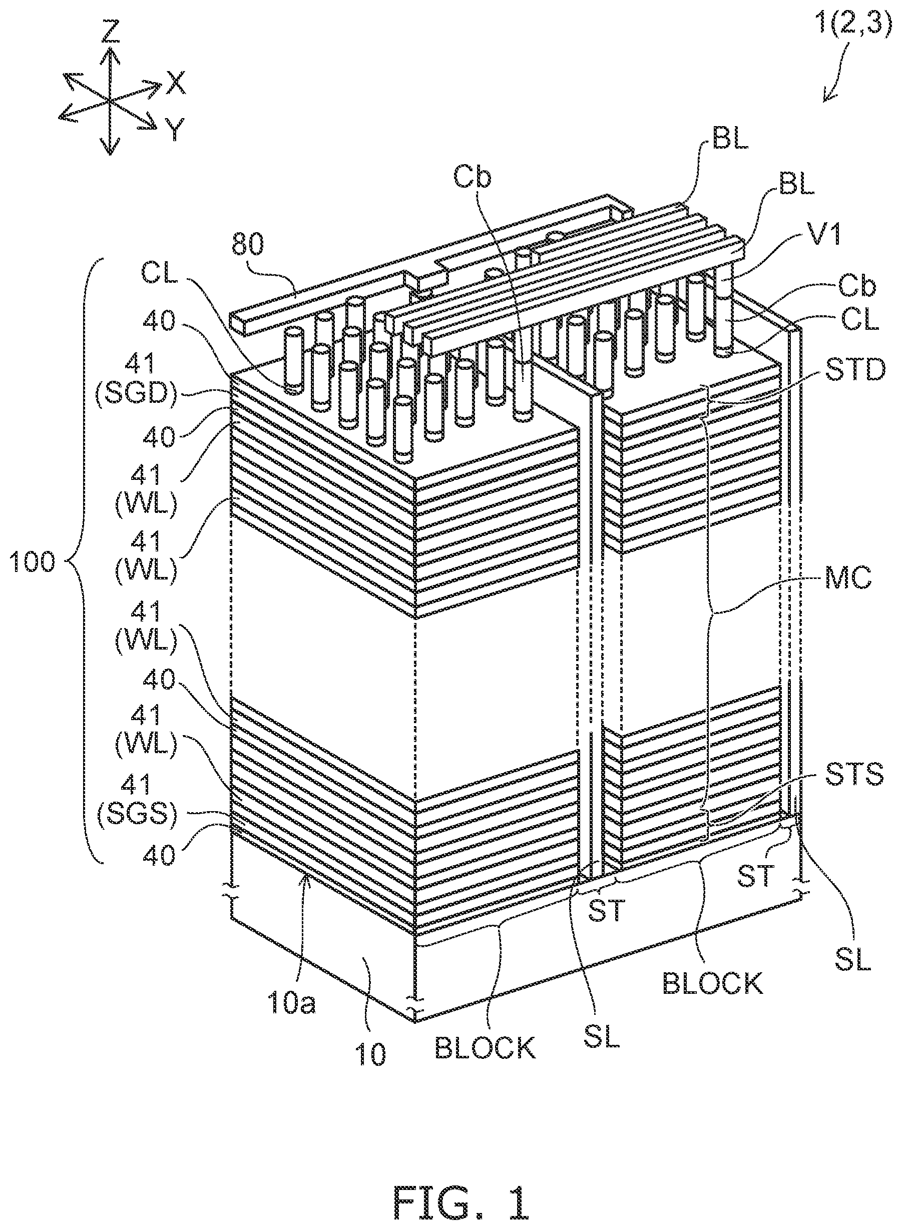
is a schematic perspective view of a memory cell array of a semiconductor device of a first embodiment.
As shown in , in the semiconductor device of the first embodiment, two directions which are parallel to a major surface 10 a of a substrate 10 and orthogonal to each other are an X-direction and a Y-direction, and a direction which is orthogonal to these X-direction and Y-direction is a Z-direction. For example, the Z-direction corresponds to a first direction, the X-direction corresponds to a second direction, and the Y-direction corresponds to a third direction.
A memory cell array 1 of the semiconductor device of the first embodiment includes a stacked body 100 including a plurality of electrode layers 41 , a plurality of columnar portions CL, and a plurality of separating portions ST. The plurality of electrode layers 41 are stacked on the major surface 10 a of the substrate 10 so as to be separated from each other. The number of plurality of stacked electrode layers 41 is arbitrary. For example, each of the plurality of electrode layers 41 includes doped silicon. The doped silicon includes, for example, one or more materials selected from the group consisted of phosphorus, arsenic, and boron.
For example, the higher the impurity concentrations of the plurality of electrode layers 41 , the farther from the substrate 10 the electrode layers 41 are. For example, the impurity concentration of the electrode layer 41 closest to the substrate 10 is about 1×10 20 cm −3 , and the impurity concentration of the electrode layer 41 farthest from the substrate 10 is about 3×10 20 cm −3 .
For example, each of the plurality of electrode layers 41 may include metal such as tungsten or molybdenum.
An insulator 40 is disposed among a plurality of electrode layers 41 . The insulator 40 may be, for example, an insulating material such as a silicon oxide film, or may be an air gap.
A plurality of electrode layers 41 include a drain-side select gate electrode SGD, a plurality of word lines WL, and a source-side select gate electrode SGS.
For example, the source-side select gate electrode SGS is provided on the substrate 10 . For example, the plurality of word lines WL are provided on the source-side select gate electrode SGS. For example, the drain-side select gate electrode SGD is provided on the plurality of word lines WL.
The drain-side select gate electrode SGD functions as a gate electrode of the drain-side select transistor STD. The source-side select gate electrode SGS functions as a gate electrode of the source-side select transistor STS. A plurality of memory cells MC are connected in series between the drain-side select transistor STD and the source-side select transistor STS. One word line WL functions as a gate electrode of one memory cell MC.
The stacked body 100 includes a plurality of separating portions ST. The separating portions ST extend inside the stacked body 100 in the Z-direction and the Y-direction. The separating portion ST separates the stacked body 100 in the X-direction. The region separated by the separating portion ST is called “block”. The block is, for example, a minimum unit of information erase. The erase size is set for one block or a plurality of blocks which are combined.
A source layer SL is provided in the separating portion ST. The source layer SL is insulated from the stacked body 100 , and spreads like a plate, for example, in the Z-direction and the Y-direction. An upper layer wiring 80 is provided above the source layer SL. The upper layer wiring 80 extends in the X-direction. The upper layer wiring 80 is electrically connected to a plurality of source layers SL which are arranged in the X-direction.
A plurality of columnar portions CL are provided in the stacked body 100 separated by the separating portion ST. The columnar portions CL extend in the stacked body 100 in the Z-direction.
The columnar portions CL are disposed in the form of, for example, a houndstooth pattern or a square lattice pattern, in the memory cell array 1 .
A plurality of bit lines BL are provided above the upper end portion of the columnar portions CL. The plurality of bit lines BL extend in the X-direction. The upper end portion of the columnar portions CL are electrically connected to one of the bit lines BL through the contact portion Cb and the contact portion V 1 .
is a schematic sectional view of the memory cell array of the semiconductor device of the first embodiment. corresponds to a part of the cross section parallel to the XZ plane in . is a schematic sectional view obtained by extracting the columnar portion CL and its surrounding portion. is a schematic sectional view taken along line III-III in . is a schematic sectional view taken along line IV-IV in .
As shown in , a plurality of electrode layers 41 include, for example, a first electrode layer 41 a , a second electrode layer 41 b , and a third electrode layer 41 c . The second electrode layer 41 b is disposed between the first electrode layer 41 a and the substrate 10 . The third electrode layer 41 c is disposed between the first electrode layer 41 a and the second electrode layer 41 b.
As shown in to 4 , the columnar portion CL extends in the stacked body 100 in the Z-direction and is electrically connected to the substrate 10 . For example, the columnar portion CL has a substantially columnar shape. For example, the columnar portion CL has a tapered shape. In other words, the smaller the diameter of the columnar portion CL, the closer to the substrate 10 the columnar portion CL is.
The columnar portion CL includes a core portion 51 and a semiconductor body 52 . The core portion 51 extends in the stacked body 100 in the Z-direction. The semiconductor body 52 is provided between the core portion 51 and the stacked body 100 and between the core portion 51 and the substrate 10 .
A plurality of charge storage portions 32 are provided between the columnar portions CL and the plurality of electrode layers 41 . For example, the charge storage portions 32 are floating gates or charge trapping layers. An insulator 40 is disposed among the plurality of charge storage portions 32 . The respective charge storage portions 32 are spaced apart in the Z-direction by the insulator 40 . For example, the smaller the thickness of the charge storage portion 32 between the columnar portion CL and the electrode layer 41 , the closer to the substrate 10 the charge storage portion 32 is.
In the specification, the thickness of the charge storage portion 32 is the thickness of the charge storage portion 32 in the direction in the X-direction between the columnar portion CL and the electrode layer 41 .
The plurality of charge storage portions 32 include for example, a first charge storage portion 32 a , a second charge storage portion 32 b , and a third charge storage portion 32 c . For example, the first charge storage portion 32 a is disposed between the columnar portion CL and the first electrode layer 41 a . For example, the second charge storage portion 32 b is disposed between the columnar portion CL and the second electrode layer 41 b . For example, the third charge storage portion 32 c is disposed between the columnar portion CL and the third electrode layer 41 c.
For example, the thickness L 1 of the first charge storage portion 32 a in the X-direction between the columnar portion CL and the first electrode layer 41 a is thicker than the thickness L 2 of the second charge storage portion 32 b in the X-direction between the columnar portion CL and the second electrode layer 41 b.
For example, the thickness L 3 of the third charge storage portion 32 c in the X-direction between the columnar portion CL and the third electrode layer 41 c is a thickness not more than the thickness L 1 . For example, the thickness L 3 is a thickness not less than the thickness L 2 .
A tunnel insulating film 31 is provided between the columnar portion CL and each charge storage portion 32 and between the columnar portion CL and the insulator 40 . For example, the tunnel insulating film 31 is cylindrical. For example, the smaller the inner diameter of the tunnel insulating film 31 , the closer to the substrate 10 the tunnel insulating film 31 is.
For example, the inner diameter D 1 of the tunnel insulating film 31 between the columnar portion CL and the first charge storage portion 32 a is larger than the inner diameter D 2 of the tunnel insulating film 31 between the columnar portion CL and the second charge storage portion 32 b.
For example, the size of the inner diameter D 3 of the tunnel insulating film 31 between the columnar portion CL and the third charge storage portion 32 c is not more than the size of the inner diameter D 1 . The size of the inner diameter D 3 is not less than the size of the inner diameter D 2 .
A block insulating film 33 is provided between the charge storage portion 32 and the electrode layer 41 . For example, a plurality of block insulating films 33 are provided for respective electrode layers 41 .
Examples of the plurality of block insulating films 33 include a first block insulating film 33 a , a second block insulating film 33 b , and a third block insulating film 33 c . The first block insulating film 33 a is disposed between the first charge storage portion 32 a and the first electrode layer 41 a . The second block insulating film 33 b is disposed between the second charge storage portion 32 b and the second electrode layer 41 b . The third block insulating film 33 c is disposed between the third charge storage portion 32 c and the third electrode layer 41 c.
The charge storage portion 32 includes for example, silicon. In a case of a floating gate, the charge storage portion 32 stores charges. In a case of a charge trapping layer, the charge storage portion 32 has a trapping site for trapping charges and traps charges. The threshold of the memory cell MC varies depending on the amount of charge present in the charge storage portion. Thus, the memory cell MC stores information. The tunnel insulating film 31 includes for example, silicon oxide. The tunnel insulating film 31 is a potential barrier between the charge storage portion 32 and the semiconductor body 52 . The tunnel insulating film 31 tunnels charges when charges are injected into the charge storage portion 32 from the semiconductor body 52 (write operation), and when charges are diffused from the charge storage portion 32 to the semiconductor body 52 (erase operation). The block insulating film 33 may contain for example, aluminum oxide, may contain silicon oxide, or may be a stacked film thereof. The block insulating film 33 suppresses tunneling from the charge storage portion 32 to the word line during the write operation, and suppresses back tunneling of charges from the word line WL to the charge storage portion 32 during the erase operation.
Assuming that the capacitance of the block insulating film 33 is C IPD and the capacitance of the tunnel insulating film 31 is C ox , when the voltage (write voltage) applied to the word line WL during the write operation is V PGM , the voltage V TNL applied to the tunnel insulating film during the write operation can be represented by, for example, V TNL =( C IPD /( C IPD +C ox ))× V PGM (1). In Equation (1), C IPD /(C IPD +C ox ) is called “coupling ratio”.
is a graph illustrating the relationship between the diameter of the columnar portion and the coupling ratio. is a graph showing the diameter of the columnar portion CL on the horizontal axis and the coupling ratio on the vertical axis. The solid line shows data when the thickness of each charge storage portion 32 between the columnar portion CL and the electrode layer 41 is 10 nm. The broken line shows data when the thickness of each charge storage portion 32 between the columnar portion CL and the electrode layer 41 is 5 nm.
For example, a configuration in which the columnar portion CL has a tapered shape and the thickness of each charge storage portion 32 between the columnar portion CL and the electrode layer 41 is constant may be considered. In this case, as the diameter of the columnar portion CL decreases, a difference between the inner diameter of the block insulating film 33 and the inner diameter of the tunnel insulating film 31 increases. For example, variations in the difference between the circumferential length of the block insulating film 33 and the circumferential length of the tunnel insulating film 31 are increased between the upper and lower layers of the memory cell array. Therefore, the coupling ratio of the corresponding region changes depending on the diameter of the columnar portion CL. As shown in , as the diameter of the columnar portion CL decreases, the coupling ratio of the corresponding region increases. For example, a difference ΔC in coupling ratios occurs between a region where the diameter of the columnar portion CL is small and a region where the diameter of the columnar portion CL is large. This results in that variations in the coupling ratio occur between the upper and lower layers of the memory cell array. This results in that variations in the writing speed occur between the upper and lower layers of the memory cell array. During a read operation, read disturb is remarkable.
As shown in , the coupling ratio in the region where the columnar portion CL is large when the thickness of the charge storage portion 32 is 10 nm shows approximately the same value as the coupling ratio in the region where the columnar portion CL is small when the thickness of the charge storage portion 32 is 5 nm. In the first example, the thickness of the charge storage portion 32 in the region where the diameter of the columnar portion CL is small is shorter than the thickness of the charge storage portion 32 in the region where the diameter of the columnar portion CL is large. With such a configuration, the difference ΔC in coupling ratios between the upper and lower layers of the memory cell can be reduced.
For example, as the diameter of the columnar portion CL decreases, the ratio between the inner diameter of the block insulating film 33 and the inner diameter of the tunnel insulating film 31 is suppressed from increasing. Therefore, the variation in the ratio between the circumferential length of the block insulating film 33 and the circumferential length of the tunnel insulating film 31 is suppressed between the upper and lower layers of the memory cell array. Thus, variations in the coupling ratio between the upper and lower layers of the memory cell array are suppressed. For example, variations in writing speed between the upper and lower layers of the memory cell array can be suppressed. In addition, read disturb and write disturb can be suppressed.
In the first embodiment, in a case where each electrode layer 41 contains doped silicon, the higher the impurity concentration of the electrode layer 41 , the farther from the substrate 10 the electrode layer 41 is. Thus, the lower the resistivity of the electrode layer 41 , the farther from the substrate 10 the electrode layer 41 is. For example, it is possible to correct the signal propagation delay of the word line caused by the difference in word line resistance, due to a difference between the memory hole diameters of the upper and lower layers of the memory cell array, by controlling the resistivity of the electrode layer 41 .
Manufacturing Method
to 13 are schematic sectional views showing a manufacturing method of the semiconductor device of the first embodiment. to 13 correspond to the cross section shown in .
As shown in , the insulator 40 which is a first layer and the electrode layer 41 which is a second layer are alternately stacked on the substrate 10 . Thus, the stacked body 100 including the electrode layer 41 stacked on the substrate 10 with the insulator 40 interposed therebetween is formed. The insulator 40 is formed of, for example, a material containing silicon oxide. For example, the electrode layer 41 is formed of a material containing doped silicon. The doped silicon includes, for example, one or more materials selected from the group consisted of phosphorus, arsenic, and boron. For example, the higher the impurity concentration of the electrode layer 41 , the farther from the substrate 10 the electrode layer 41 is. For example, the electrode layer 41 may be formed of a material containing metal such as tungsten.
As shown in , for example, a memory hole MH 1 is formed in the stacked body 100 by a photolithography method. The memory hole MH 1 extends in the Z-direction in the stacked body 100 . The memory hole MH 1 penetrates the stacked body 100 and reaches the upper surface of the substrate 10 . For example, the memory hole MH 1 has a tapered shape. For example, the smaller the diameter of the memory hole MH 1 , the closer to the substrate 10 the memory hole MH 1 is.
As shown in , a sacrificial member 50 a is formed in the memory hole MH 1 . For example, the sacrificial member 50 a is formed at the lower part of the memory hole MH 1 .
As shown in , an etching process is performed on the end face of the electrode layer 41 exposed in the memory hole MH 1 . For example, an etchant is supplied into the memory hole MH 1 . Thus, the end face of the electrode layer 41 exposed in the memory hole MH 1 retreats. At this time, the lower part of the memory hole MH 1 is filled with the sacrificial member 50 a . Therefore, the electrode layer 41 in the lower part of the memory hole MH 1 is not etched.
As shown in , the sacrificial member 50 a is removed by an etching process such as chemical dry etching or wet etching.
As shown in , an etching process is performed on the end face of the electrode layer 41 exposed in the memory hole MH 1 . For example, etchant is supplied into the memory hole MH 1 . Thus, the end face of the electrode layer 41 exposed in the memory hole MH 1 retreats.
By performing the processes shown in , the retreat amount of the end face of the electrode layer 41 increases as the distance from the substrate 10 increases. Note that in the case where the retreat amount of the end face of the electrode layer 41 can be controlled according to the conditions of the etching process or the like, the sacrificial member 50 a may not be formed. For example, when the electrode layer 41 contains silicon and impurity, the etching rate may be controlled by changing the impurity concentration for each electrode layer 41 .
Next, as shown in , the block insulating film 33 is formed on the inner wall of the space generated by the retraction of the electrode layer 41 . The block insulating film 33 is formed of, for example, a material containing aluminum oxide. The block insulating film 33 may be formed of a material containing, for example, silicon oxide. Thereafter, the charge storage portion 32 is formed in the space by the retraction of the electrode layer 41 . The charge storage portion 32 is formed of a material containing, for example, polysilicon or silicon nitride. Further, the block insulating film 33 and the charge storage portion 32 are etched back by chemical dry etching or the like up to a place where there is no step from the memory hole MH 1 and they are aligned with the insulator 40 , and are separated for each layer. Thus, the space generated by the retraction of the electrode layer 41 is filled with the block insulating film 33 and the charge storage portion 32 .
As shown in , the tunnel insulating film 31 is formed on the inner wall of the memory hole MH 1 . The tunnel insulating film 31 is formed of at least one material selected from the group consisted of for example, silicon oxide, silicon oxynitride, and silicon nitride. The tunnel insulating film 31 may be formed as a stacked film including a silicon oxide film, a silicon oxynitride film, and a silicon nitride film.
As shown in , the semiconductor film 52 a is formed on the tunnel insulating film 31 . The tunnel insulating film 31 and the semiconductor film 52 a formed at the bottom of the memory hole MH 1 are removed by anisotropic etching. At this time, the tunnel insulating film 31 and the semiconductor film 52 a formed on the side wall of the memory hole MH 1 remain. The tunnel insulating film 31 formed on the side wall of the memory hole MH 1 is protected from the influence of anisotropic etching by the semiconductor film 52 a formed thereon.
Thereafter, the semiconductor body 52 is formed in the memory hole MH 1 as shown in . The semiconductor body 52 is electrically connected to the substrate 10 . The semiconductor film 52 a is a part of the semiconductor body 52 . Thereafter, the core portion 51 is formed in the memory hole MH 1 . The core portion 51 is formed of, for example, a material containing silicon oxide. The memory hole MH 1 is filled with the semiconductor body 52 and the core portion 51 .
The semiconductor device of the first embodiment can be manufactured by, for example, such a manufacturing method.
In the manufacturing method of the semiconductor device of the first embodiment, the sacrificial member 50 a is formed in the memory hole MH 1 . Thus, the retreat amount of the end face of the electrode layer 41 is controlled, as shown in .
In the manufacturing method of the semiconductor device of the first embodiment, the impurity concentration may be changed for each electrode layer 41 . For example, the farther from the substrate 10 , the higher the impurity concentration of the electrode layer 41 may be. Thus, the etching rate of the electrode layer 41 can be controlled. For example, when performing the processes shown in , the etching conditions are relaxed. For example, it is possible to control the retreat amount of the end face of the electrode layer 41 without forming the sacrificial member 50 a.
is a schematic perspective view of a memory cell array of a semiconductor device of another example of the first embodiment.
Although the memory cell array is formed on the substrate 10 in the above example, a buried source line electrode containing polysilicon or tungsten may be formed flat on a peripheral circuit formed on a silicon substrate, and a memory cell array may be formed on the buried source line electrode.
In this case, a peripheral circuit 11 is provided on the major surface 10 a of the substrate 10 as shown in . The peripheral circuit 11 includes a transistor Tr provided in the insulating film. A source line electrode 12 (a buried source line electrode) is provided on the peripheral circuit 11 . An insulating film 13 is provided on the source line electrode 12 . A semiconductor layer 14 is provided on the insulating film 13 . The stacked body 100 is provided on the semiconductor layer 14 .
Second Embodiment
Semiconductor Device
is a schematic sectional view of the memory cell array of the semiconductor device of the first embodiment. corresponds to a part of a cross section parallel to the XZ plane in . is a schematic sectional view obtained by extracting the columnar portion CL and its surrounding portion.
As shown in , a memory cell array 2 of the semiconductor device of the first embodiment includes a stacked body 100 , a columnar portion CL, a tunnel insulating film 31 , a plurality of charge storage portions 32 , and a plurality of block insulating films 33 .
The stacked body 100 includes a plurality of electrode layers 41 stacked on a substrate 10 in the Z-direction with an insulator 40 interposed therebetween. The stacked body 100 includes a stacked portion 100 a including a part of the plurality of electrode layers 41 and a stacked portion 100 b including another part of the plurality of electrode layers 41 . The stacked portion 100 a is provided on the substrate 10 . The stacked portion 100 b is provided between the substrate 10 and the stacked portion 100 a.
The columnar portion CL extends in the stacked body 100 in the Z-direction. The columnar portion CL includes a first columnar portion CLa provided in the stacked portion 100 a and a second columnar portion CLb provided in the stacked portion 100 b.
For example, the first columnar portion CLa and the second columnar portion CLb each have a tapered shape. For example, the smaller the diameter of the first columnar portion CLa, the closer to the substrate 10 the first columnar portion CLa is. The smaller the diameter of the second columnar portion CLb, the closer to the substrate 10 the second columnar portion CLb is. For example, the diameter of the lower end of the first columnar portion CLa is smaller than the diameter of the upper end of the second columnar portion CLb.
The plurality of charge storage portions 32 are provided between the columnar portion CL and the plurality of electrode layers 41 . In the stacked portion 100 a , the shorter the thickness of the charge storage portion 32 between the columnar portion CL and one electrode layer 41 , the closer to the stacked portion 100 b the charge storage portion 32 is. In the stacked portion 100 b , the smaller the thickness of the charge storage portion 32 between the columnar portion CL and one electrode layer 41 , the closer to the substrate 10 the charge storage portion 32 is.
Examples of the plurality of electrode layers 41 include a first electrode layer 41 a , a second electrode layer 41 b , a third electrode layer 41 c , a fourth electrode layer 41 d , a fifth electrode layer 41 e , and a sixth electrode layer 41 f.
The first electrode layer 41 a , the second electrode layer 41 b , and the fifth electrode layer 41 e are included in the stacked portion 100 a . The third electrode layer 41 c , the fourth electrode layer 41 d , and the sixth electrode layer 41 f are included in the stacked portion 100 b.
The second electrode layer 41 b is disposed between the first electrode layer 41 a and the stacked portion 100 b . The fourth electrode layer is disposed between the third electrode layer 41 c and the substrate 10 . The fifth electrode layer 41 e is disposed between the first electrode layer 41 a and the third electrode layer 41 c . The sixth electrode layer 41 f is disposed between the third electrode layer 41 c and the fourth electrode layer 41 d.
Examples of the plurality of charge storage portions 32 include a first charge storage portion 32 a , a second charge storage portion 32 b , a third charge storage portion 32 c , a fourth charge storage portion 32 d , a fifth charge storage portion 32 e , and a sixth charge storage portion 32 f.
The first charge storage portion 32 a is disposed between the first columnar portion CLa and the first electrode layer 41 a . The second charge storage portion 32 b is disposed between the first columnar portion CLa and the second electrode layer 41 b . The third charge storage portion 32 c is disposed between the second columnar portion CLb and the third electrode layer 41 c . The fourth charge storage portion 32 d is disposed between the second columnar portion CLb and the fourth electrode layer 41 d . The fifth charge storage portion 32 e is disposed between the first columnar portion CLa and the fifth electrode layer 41 e . The sixth charge storage portion 32 f is disposed between the second columnar portion CLb and the sixth electrode layer 41 f.
The thickness L 4 in the X-direction of the first charge storage portion 32 a between the first electrode layer 41 a and the first columnar portion CLa is thicker than the thickness L 5 in the X-direction of the second charge storage portion 32 b between the second electrode layer 41 b and the first columnar portion CLa. The thickness L 6 in the X-direction of the third charge storage portion 32 c between the third electrode layer 41 c and the second columnar portion CLb is thicker than the thickness L 7 in the X-direction of the fourth charge storage portion 32 d between the fourth electrode layer 41 d and the second columnar portion CLb. The thickness L 5 is smaller than the thickness L 6 .
The thickness L 8 in the X-direction of the fifth charge storage portion 32 e between the fifth electrode layer 41 e and the first columnar portion CLa is a thickness not more than the thickness L 4 , and the thickness L 8 is a thickness not less than the thickness L 5 . The thickness L 9 in the X-direction of the sixth charge storage portion 32 f between the sixth electrode layer 41 f and the second columnar portion CLb is a thickness not more than the thickness L 6 , and the thickness L 9 is a thickness not less than the thickness L 7 .
The block insulating film 33 is provided between the electrode layer 41 and the charge storage portion 32 . Examples of the plurality of block insulating films 33 include a first block insulating film 33 a , a second block insulating film 33 b , a third block insulating film 33 c , a fourth block insulating film 33 d , a fifth block insulating film 33 e , and a sixth block insulating film 33 f.
The first block insulating film 33 a is disposed between the first charge storage portion 32 a and the first electrode layer 41 a . The second block insulating film 33 b is disposed between the second charge storage portion 32 b and the second electrode layer 41 b . The third block insulating film 33 c is disposed between the third charge storage portion 32 c and the third electrode layer 41 c . The fourth block insulating film 33 d is disposed between the fourth charge storage portion 32 d and the fourth electrode layer 41 d . The fifth block insulating film 33 e is disposed between the fifth charge storage portion 32 e and the fifth electrode layer 41 e . The sixth block insulating film 33 f is disposed between the sixth charge storage portion 32 f and the sixth electrode layer 41 f.
A tunnel insulating film 31 is provided between the columnar portion CL and the charge storage portion 32 and between the columnar portion CL and the insulator 40 . For the example, the smaller the inner diameter of the tunnel insulating film 31 between the first columnar portion CLa and the charge storage portion 32 , the closer to the stacked portion 100 b the tunnel insulating film 31 is. For example, the smaller the inner diameter of the tunnel insulating film 31 between the second columnar portion CLb and the charge storage portion 32 , the closer to the substrate 10 the tunnel insulating film 31 is. The inner diameter of the tunnel insulating film 31 provided around the lower end of the first columnar portion CLa is smaller than the inner diameter of the tunnel insulating film 31 provided around the upper end of the second columnar portion CLb.
For example, the size of the inner diameter D 4 of the tunnel insulating film 31 between the first columnar portion CLa and the first charge storage portion 32 a is larger than the size of the inner diameter D 5 of the tunnel insulating film 31 between the first columnar portion CLa and the second charge storage portion 32 b . For example, the size of the inner diameter D 6 of the tunnel insulating film 31 between the second columnar portion CLb and the third charge storage portion 32 c is larger than the size of the inner diameter D 7 of the tunnel insulating film 31 between the second columnar portion CLb and the fourth charge storage portion 32 d . For example, the size of the inner diameter D 6 is larger than the size of the inner diameter D 5 .
For example, the size of the inner diameter D 8 of the tunnel insulating film 31 between the first columnar portion CLa and the fifth charge storage portion 32 e is not more than the inner diameter D 4 . The size of the inner diameter D 8 is not less than the size of the inner diameter D 5 . For example, the size of the inner diameter D 9 of the tunnel insulating film 31 between the second columnar portion CLb and the sixth charge storage portion 32 f is not more than the inner diameter D 6 . The size of the inner diameter D 9 is not less than the size of the inner diameter D 7 .
In the case where the electrode layer 41 contains silicon and impurity, the impurity concentration may vary for each electrode layer 41 in each stacked portion (the stacked portion 100 a and the stacked portion 100 b ). For example, in a case where the electrode layer 41 included in the stacked portion 100 a contains silicon and impurity, the higher the impurity concentration, the farther from the stacked portion 100 b the electrode layer 41 is. In the case where the electrode layer 41 included in the stacked portion 100 b contains silicon and impurity, the higher the impurity concentration may be, the farther from the substrate 10 the electrode layer 41 is.
In the semiconductor device of the second embodiment, the smaller the thickness of each charge storage portion 32 between the columnar portion CL and the electrode layer 41 , the smaller the diameter of the corresponding tunnel insulating film 31 . This prevents the difference between the inner diameter of the block insulating film 33 and the inner diameter of the tunnel insulating film 31 from increasing. Thus, the variations in the coupling ratio are suppressed between the upper and lower layers of the memory cell array. For example, the variations in the write speed can be suppressed between the upper and lower layers of the memory cell array. In addition, it is possible to suppress read disturb and write disturb. This improves the stability of the write operation and the read operation.
In the second embodiment, the impurity concentration of the electrode layer 41 may be changed in the respective stacked portions (the stacked portion 100 a and the stacked portion 100 b ). Therefore, the lower the resistivity of the electrode layer 41 , the higher the impurity concentration of the electrode layer 41 . For example, the larger the diameter of the portion of the tunnel insulating film 31 corresponding to the electrode layer 41 , the lower the resistivity may be. For example, it is possible to correct the signal propagation delay of the word line caused by the difference in word line resistance, due to a difference between the memory hole diameters of the upper and lower layers of the memory cell array, by controlling the resistivity of the electrode layer 41 .
Manufacturing Method
to 21 are schematic sectional views showing the manufacturing method of the semiconductor device of the second embodiment. to 21 correspond to the cross section shown in .
First, the processes shown in to 11 are performed in the same manner as in the first embodiment. Thus, the stacked portion 100 b having a memory hole MH 1 , the charge storage portion 32 , and the block insulating film 33 are formed, as shown in . The stacked portion 100 b corresponds to the stacked body 100 shown in . A sacrificial member 61 is formed in the memory hole MH 1 . The memory hole MH 1 is filled with the sacrificial member 61 .
As shown in , the insulator 40 which is a third layer and the electrode layer 41 which is a fourth layer are stacked alternately on the stacked portion 100 b . Thereby, the stacked portion 100 a is formed on the stacked portion 100 b.
In the stacked portion 100 b , for example, the electrode layer 41 is formed of a material containing doped silicon. Examples of the doped silicon include one or more materials selected from the group consisted of phosphorus, arsenic, and boron. For example, the higher the impurity concentration of the electrode layer 41 may be, the farther from the stacked portion 100 b the electrode layer 41 is. For example, the electrode layer 41 may be formed of a material containing a metal such as tungsten or molybdenum.
As shown in , a memory hole MH 2 is formed on the sacrificial member 61 . The memory hole MH 2 penetrates the stacked portion 100 a in the Z-direction. The upper surface of the sacrificial member 61 is exposed at the bottom of the memory hole MH 2 .
As shown in , a sacrificial member 50 b is formed in the memory hole MH 2 . For example, the sacrificial member 50 b is formed in the lower part of the memory hole MH 1 . Thereafter, an etching process is performed on the end face of the electrode layer 41 exposed in the memory hole MH 2 . For example, an etchant is supplied into the memory hole MH 2 . Thus, the end face of the electrode layer 41 exposed in the memory hole MH 2 retreats. At this time, the end portion of the electrode layer 41 in the lower part of the memory hole MH 2 is covered with the sacrificial member 50 b . Therefore, the end portion of the electrode layer 41 in the lower part of the memory hole MH 2 is not etched.
As shown in , the sacrificial member 50 b is removed by an etching process such as chemical dry etching. Thereafter, an etching process is performed on the exposed face of the electrode layer 41 . For example, an etchant is supplied into the memory hole MH 2 . Thus, the end face of the electrode layer 41 exposed in the memory hole MH 2 retreats.
By performing the processes shown in , the retreat amount of the end face of the electrode layer 41 of the stacked portion 100 a increases as the distance from the stacked portion 100 b increases. Note that in the case where the retreat amount of the end face of the electrode layer 41 can be controlled according to the conditions of the etching process or the like, the sacrificial member 50 b may not be formed. For example, in a case where the electrode layer 41 contains silicon and impurity, the etching rate may be controlled by changing the impurity concentration for each electrode layer 41 .
As shown in , a block insulating film 33 is formed on the inner wall of the space generated by the retraction of the electrode layer 41 of the stacked portion 100 a . The block insulating film 33 is formed of, for example, a material containing aluminum oxide. The block insulating film 33 may be formed of, for example, a material containing silicon oxide. Thereafter, a charge storage portion 32 is formed in the space generated by the retraction of the electrode layer 41 of the stacked portion 100 a . The charge storage portion 32 is formed of, for example, a material containing polysilicon or silicon nitride. Further, the block insulating film 33 and the charge storage portion 32 are etched back by chemical dry etching or the like up to a place where there is no step from the memory holes MH 1 and MH 2 and they are aligned with the insulator 40 , and are separated for each layer. Thus, the block insulating film 33 and the charge storage portion 32 are formed in the stacked portion 100 a . Thereafter, a sacrificial member 50 a is removed by an etching process such as chemical dry etching.
As shown in , the tunnel insulating film 31 is formed on the side wall of the memory holes MH 1 and MH 2 . A columnar portion CL is formed in the memory holes MH 1 and MH 2 .
The semiconductor device of the second embodiment can be manufactured by for example, such a manufacturing method.
Third Embodiment
Semiconductor Device
is a schematic sectional view of a memory cell array of a semiconductor device of a third embodiment. corresponds to a part of the cross section parallel to the XZ plane in . is a schematic sectional view obtained by extracting a columnar portion CL and its surrounding portions.
As shown in , in the memory cell array 3 of the semiconductor device of the third embodiment, a block insulating film 33 is formed between a charge storage portion 32 and an electrode layer 41 , and between the electrode layer 41 and an insulator 40 . The block insulating film 33 may not be provided between the charge storage portion 32 and the insulator 40 . The other configuration is the same as for example, the semiconductor device of the first embodiment. An insulator 70 is provided between the side wall of a separating portion ST and a source layer SL. The insulator 70 contains for example, silicon oxide.
Similar to the first example, the smaller the thickness of each charge storage portion 32 between the columnar portion CL and the electrode layer 41 , the closer to the substrate 10 the charge storage portion 32 is. This prevents the difference between the inner diameter of the block insulating film 33 and the inner diameter of a tunnel insulating film 31 from increasing between the upper and lower layers of the memory cell array. This suppresses variations in the coupling ratio between the upper and lower layers of the memory cell array. For example, the variations in the write speed can be suppressed between the upper and lower layers of the memory cell array. In addition, it is possible to suppress read disturb and write disturb. This improves the stability of the write operation and the read operation.
Similar to the first embodiment, in a case where each electrode layer 41 contains doped silicon, the higher the impurity concentration of the electrode layer 41 may be, the farther from the substrate 10 the electrode layer 41 is. Thus, the lower the resistivity of the electrode layer 41 , the farther from the substrate 10 the electrode layer 41 is. For example, it is possible to correct the signal propagation delay of the word line caused by the difference in word line resistance, due to a difference between the memory hole diameters of the upper and lower layers of the memory cell array, by controlling the resistivity of the electrode layer 41 .
Manufacturing Method
to 26 are schematic sectional views showing the manufacturing method of the semiconductor device of the third embodiment. to 26 correspond to the cross section shown in .
First, the processes shown in are performed. In the third embodiment, the insulator 40 which is a first layer and a replacement member 42 which is a second layer are alternately stacked on the substrate 10 . Thereby, a stacked portion 100 is formed on the substrate 10 . For example, the small the density of the replacement member 42 may be, the farther from the substrate 10 the replacement member 42 is.
The replacement member 42 is a layer which is later replaced by the electrode layer 41 . The material of the replacement member 42 is selected from materials different from the insulator 40 , of which the etching selection ratio can be obtained for the insulator 40 . For example, when silicon oxide is selected as the insulator 40 , silicon nitride is selected for the replacement member 42 .
A memory hole MH 1 is formed in the stacked body 100 by performing the processes shown in . After that, the end face of the replacement member 42 exposed in the memory hole MH 1 is etched by performing the processes shown in to 10 . Thus, the end portion of the replacement member 42 retreats. In a case where the retreat amount of the end face of the replacement member 42 can be controlled according to the conditions of the etching process or the like, formation of the sacrificial member 50 a may be omitted. For example, the etching rate may be controlled by controlling the density of the replacement member 42 .
Thereafter, as shown in , the charge storage portion 32 is formed in the space generated by the retraction of the end portion of the replacement member 42 , and the charge storage portion 32 is etched back by chemical dry etching or the like up to a place where there is no step from the memory hole MH 1 and it is aligned with the insulator 40 , and is separated for each layer.
As shown in , the tunnel insulating film 31 is formed on the side wall of the memory hole MH 1 . Thereafter, the columnar portion CL is formed in the memory hole MH 1 .
As shown in , the separating portion ST is formed in the stacked body 100 . The separating portion ST is formed, for example, by performing anisotropical etching on the stacked body 100 . Thereafter, the replacement member 42 is removed. The replacement member 42 is removed, for example, by a wet etching process through the separating portion ST.
As shown in , the block insulating film 33 is formed on the inner wall of the space generated by removing the replacement member 42 . The electrode layer 41 is formed in the space generated by removing the replacement member 42 . After that, as shown in , the insulator 70 is formed on the side wall of the separating portion ST. The source layer SL is formed in the separating portion ST.
The semiconductor device of the third embodiment can be manufactured by, for example, such a manufacturing method.
As described above, according to the embodiment, a semiconductor device capable of suppressing variations in the coupling ratio can be obtained.
While certain embodiments have been described, these embodiments have been presented by way of example only, and are not intended to limit the scope of the inventions. Indeed, the novel embodiments described herein may be embodied in a variety of other forms; furthermore, various omissions, substitutions and changes in the form of the embodiments described herein may be made without departing from the spirit of the inventions. The accompanying claims and their equivalents are intended to cover such forms or modification as would fall within the scope and spirit of the inventions.
Figures (18)
Citations
This patent cites (14)
- US9716105
- US20070252201
- US20100001931
- US20100163968
- US20130009229
- US20140264527
- US20150318298
- US20160055911
- US20160190313
- US20160233343
- US20160300849
- US20170076807
- US104981904
- US2010-157734