Module Board and Memory Module Including the Same
Abstract
A module board and a memory module are provided. The module board includes a first branch line for connecting a clock signal terminal disposed on at least one surface to a first branch point; a first signal line for connecting the first branch point to a first module clock signal terminal; a second signal line for connecting the first module clock signal terminal to the k th module clock signal terminal and a first termination resistance terminal; a third signal line for connecting the first branch point to a (k+1) th module clock signal terminal; and a fourth signal line for connecting the (k+1) th module clock signal terminal to a 2k th module clock signal terminal and the second termination resistance terminal, wherein a length of the third signal line is greater than a sum of a length of the first signal line and a length of the second signal line.
Claims (8)
1. A memory module comprising: a module board comprising: a plurality of stacked layers including a first layer to an nth layer, wherein n is an integer greater than one; a first module clock signal terminal to a kth module clock signal terminal arranged at a first predetermined interval in a component region of at least one surface from among an upper surface of the first layer and a lower surface of the nth layer, wherein k is an integer greater than one; a (k+1)th module clock signal terminal to a 2kth module clock signal terminal arranged at a second predetermined interval in the component region; a first termination resistance terminal disposed adjacent to the kth module clock signal terminal; a first termination resistor connected to the first termination resistance terminal; a second termination resistance terminal disposed adjacent to the 2kth module clock signal terminal; a second termination resistor connected to the second termination resistance terminal; a plurality of terminals arranged in a terminal region of the at least one surface and comprising a clock signal terminal; a first branch line for connecting the clock signal terminal disposed on the at least one surface to a first branch point; a first signal line for connecting the first branch point to the first module clock signal terminal; a second signal line for sequentially connecting the first module clock signal terminal to the kth module clock signal terminal and the first termination resistance terminal; a third signal line for connecting the first branch point to the (k+1)th module clock signal terminal; a fourth signal line for sequentially connecting the (k+1)th module clock signal terminal to the 2kth module clock signal terminal and the second termination resistance terminal; a first semiconductor memory device to a kth semiconductor memory device respectively comprising a first memory clock signal terminal to a kth memory clock signal terminal installed at the first module clock signal terminal to the kth module clock signal terminal; a (k+1)th semiconductor memory device to a 2kth semiconductor memory device respectively comprising a (k+1)th memory clock signal terminal to a 2kth memory clock signal terminal installed at the (k+1)th module clock signal terminal to the 2kth module clock signal terminal; a first module command/address terminal to a kth module command/address terminal arranged at the first predetermined interval in the component region; a (k+1)th module command/address terminal to a 2kth module command/address terminal arranged at the second predetermined interval in the component region; and a third termination resistance terminal disposed adjacent to the 2kth module command/address terminal; a fourth termination resistance terminal disposed adjacent to a (2k−1)th module command/address terminal; a second branch line for connecting the plurality of terminals disposed on the at least one surface to a second branch point; a fifth signal line for connecting the second branch point to the first module command/address terminal; a sixth signal line for sequentially connecting odd-numbered module command/address terminals comprising the first module command/address terminal to the (2k−1)th module command/address terminal and the fourth termination resistance terminal; a seventh signal line for connecting the second branch point to the (k+1)th module command/address terminal; and an eighth signal line for sequentially connecting even-numbered module command/address terminals comprising a second module command/address terminal to the 2kth module command/address terminal and the third termination resistance terminal, wherein the first semiconductor memory device to the kth semiconductor memory device further comprise respective the first memory clock signal terminal to the kth memory clock signal terminal installed at the first module command/address terminal to the kth module command/address terminal, wherein the (k+1)th semiconductor memory device to the 2kth semiconductor memory device further comprise respective (k+1)th memory clock signal terminal to 2kth memory clock signal terminal installed at the (k+1)th module command/address terminal to the 2kth module command/address terminal, wherein a length of the third signal line is greater than a sum of a length of the first signal line and a length of the second signal line, wherein the first predetermined interval is equal to the second predetermined interval, wherein the length of the second signal line is equal to a length of the fourth signal line, wherein the length of the second signal line is greater than the length of the first signal line, wherein a length of the fifth signal line is equal to a length of the seventh signal line, and wherein a sum of a length of the second branch line and the length of the fifth signal line is equal to a sum of a length of the first branch line and the length of the first signal line.
3. A memory system comprising: a control device comprising: a processor configured to generate an internal command, an internal address, and internal data by executing a program; a clock signal generator configured to generate a clock signal; a command/address generator configured to receive the internal command and the internal address from the processor based on the clock signal from the clock signal generator, and generating a command/address; and a data output interface configured to receive the internal data and generating 2k pieces of data, wherein k is an integer greater than one; and a memory module comprising: a module board comprising: a plurality of stacked layers including a first layer to an nth layer, wherein n is an integer greater than one; a first module terminal to a kth module terminal arranged at a first predetermined interval in a component region of at least one surface from among an upper surface of the first layer and a lower surface of the nth layer; a (k+1)th module terminal to a 2kth module terminal arranged at a second predetermined interval in the component region; a first termination resistance terminal disposed adjacent to the kth module terminal; a first termination resistor connected to the first termination resistance terminal, a second termination resistance terminal disposed adjacent to the 2kth module terminal; a second termination resistor connected to the second termination resistance terminal; a plurality of terminals arranged in a terminal region of the at least one surface; a first branch line for connecting at least one of the plurality of terminals to a first branch point; a first signal line for connecting the first branch point to the first module terminal; a second signal line for sequentially connecting the first module terminal to the kth module terminal and the first termination resistance terminal; a third signal line for connecting the first branch point to the (k+1)th module terminal; a fourth signal line for sequentially connecting the (k+1)th module terminal to the 2kth module terminal and the second termination resistance terminal; a first semiconductor memory device to a kth semiconductor memory device respectively comprising a first memory terminal to a kth memory terminal installed at the first module terminal to the kth module terminal; and a (k+1)th semiconductor memory device to a 2kth semiconductor memory device respectively comprising a (k+1)th memory terminal to a 2kth memory terminal installed at the (k+1)th module terminal to the 2kth module terminal, wherein a length of the third signal line is greater than a sum of a length of the first signal line and a length of the second signal line.
8. A module board comprising: a clock signal terminal; a plurality of stacked layers; a plurality of first module terminals arranged at a first predetermined interval in a component region of at least one layer among the plurality of stacked layers; a plurality of second module terminals arranged at a second predetermined interval in the component region; a first branch line connecting the clock signal terminal to a first branch point; a second branch line connecting the first branch point to the plurality of first module terminals; a third branch line connecting the first branch point to the plurality of second module terminals; a first signal line connected to the second branch line and connecting each of the plurality of first module terminals; and a second signal line connected to the third branch line and connecting each of the plurality of second module terminals, wherein a length of the first signal line is greater than a sum of a length of the second branch line and a length of the third branch line.
Show 5 dependent claims
2. The memory module of claim 1 , wherein the fifth signal line, the sixth signal line, the seventh signal line, and the eighth signal line are disposed on at least one surface of the first layer to the nth layer except for the at least one surface.
4. The memory system of claim 3 , wherein the length of the second signal line is equal to a length of the fourth signal line, and the length of the second signal line is greater than the length of the first signal line.
5. The memory system of claim 4 , wherein each of the first semiconductor memory device to the 2kth semiconductor memory device is a dual-die package (DDP) semiconductor memory device comprising a first die and a second die in a stack, each of the first die and the second die is a double data rate (DDR) semiconductor memory device, and the memory module is an unbuffered dual in-line memory module (UDIMM) or a small outline dual in-line memory module (SODIMM).
6. The memory system of claim 4 , wherein the first memory terminal to the kth memory terminal, the first module terminal to the kth module terminal, and at least one terminal transmit the clock signal or the command/address.
7. The memory system of claim 4 , wherein the first signal line, the second signal line, the third signal line, and the fourth signal line are disposed on at least one surface of the first layer to the nth layer except for the at least one surface.
Full Description
Show full text →
CROSS-REFERENCE TO THE RELATED APPLICATION
This application is a divisional application of U.S. patent application Ser. No. 17/337,850, filed on Jun. 3, 2021, which is now U.S. Pat. No. 11,477,880 issued on Oct. 18, 2022, which claims priority to Korean Patent Application No. 10-2020-0152459, filed on Nov. 16, 2020, in the Korean Intellectual Property Office, the disclosures of which are incorporated by reference herein in their entireties.
BACKGROUND
1. Field
One or more embodiments of the disclosure relate to a module board and a memory module including the same.
2. Description of the Related Art
Memory modules may include a plurality of semiconductor memory devices installed on a module board. The memory module may be classified into a server-oriented memory module and a PC-oriented (client-oriented) memory module according to whether the memory module further includes a buffer on a module board.
The server-oriented memory module includes a buffer, and thus various levels of signals applied from an external device (e.g., a central processing unit (CPU)), a graphic processing unit (GPU), or the like) may be converted (e.g., amplified) and the converted signals may be transmitted to a plurality of memory devices. Thus, in the server-oriented memory module, even if load of a plurality of semiconductor memory devices is large, the quality of a clock signal and/or a command/address may not be affected.
On the other hand, the PC-oriented memory module does not include a buffer on a module board, and thus signals applied from an external device may be transmitted to a plurality of semiconductor memory devices without converting various levels of signals. Thus, in the PC-oriented memory module, when the load of a plurality of semiconductor memory devices is large, the quality of a clock signal and/or a command/address may be degraded.
SUMMARY
One or more embodiments of the disclosure provide a module board and a memory module including the same in which, even if the load of a plurality of semiconductor memory devices is large, the quality of a clock signal and/or a command/address may not be affected.
The technical problems solved by the one or more embodiments are not limited to the above technical problems, and other technical problems which are not described herein will become apparent to those skilled in the art from the following description.
According to an embodiment, there is provided a module board including: a plurality of stacked layers including a first layer to an nth layer; a first module clock signal terminal to a kth module clock signal terminal arranged at a first predetermined interval in a component region of at least one surface from among an upper surface of the first layer and a lower surface of the nth layer; a (k+1)th module clock signal terminal to a 2kth module clock signal terminal arranged at a second predetermined interval in the component region; a first termination resistance terminal disposed adjacent to the kth module clock signal terminal; a second termination resistance terminal disposed adjacent to the 2kth module clock signal terminal; a plurality of terminals arranged in a terminal region of the at least one surface and including a clock signal terminal; a first branch line for connecting the clock signal terminal disposed on the at least one surface to a first branch point; a first signal line for connecting the first branch point to the first module clock signal terminal; a second signal line for sequentially connecting the first module clock signal terminal to the kth module clock signal terminal and the first termination resistance terminal; a third signal line for connecting the first branch point to the (k+1)th module clock signal terminal; and a fourth signal line for sequentially connecting the (k+1)th module clock signal terminal to the 2kth module clock signal terminal and the second termination resistance terminal, wherein a length of the third signal line is greater than a sum of a length of the first signal line and a length of the second signal line.
According to an embodiment, there is provided a memory module including a module board. The module board includes: a plurality of stacked layers including a first layer to an nth layer; a first module clock signal terminal to a kth module clock signal terminal arranged at a first predetermined interval in a component region of at least one surface from among an upper surface of the first layer and a lower surface of the nth layer; a (k+1)th module clock signal terminal to a 2kth module clock signal terminal arranged at a second predetermined interval in the component region; a first termination resistance terminal disposed adjacent to the kth module clock signal terminal; a first termination resistor connected to the first termination resistance terminal; a second termination resistance terminal disposed adjacent to the 2kth module clock signal terminal; a second termination resistor connected to the second termination resistance terminal; a plurality of terminals arranged in a terminal region of the at least one surface and including a clock signal terminal; a first branch line for connecting the clock signal terminal disposed on the at least one surface to a first branch point; a first signal line for connecting the first branch point to the first module clock signal terminal; a second signal line for sequentially connecting the first module clock signal terminal to the kth module clock signal terminal and the first termination resistance terminal; a third signal line for connecting the first branch point to the (k+1)th module clock signal terminal; a fourth signal line for sequentially connecting the (k+1)th module clock signal terminal to the 2kth module clock signal terminal and the second termination resistance terminal; a first semiconductor memory device to a kth semiconductor memory device respectively including a first memory clock signal terminal to a kth memory clock signal terminal installed at the first module clock signal terminal to the kth module clock signal terminal; and a (k+1)th semiconductor memory device to a 2kth semiconductor memory device respectively including a (k+1)th memory clock signal terminal to a 2kth memory clock signal terminal installed at the (k+1)th module clock signal terminal to the 2kth module clock signal terminal, wherein a length of the third signal line is greater than a sum of a length of the first signal line and a length of the second signal line.
According to an embodiment, there is provided a memory system including a control device. The control device includes: a processor configured to generate an internal command, an internal address, and internal data by executing a program; a clock signal generator configured to generate a clock signal; a command/address generator configured to receive the internal command and the internal address from the processor based on the clock signal from the clock signal generator, and generating a command/address; and a data output interface configured to receive the internal data and generating 2k pieces of data. The memory system further includes a memory module including a module board. The module board includes: a plurality of stacked layers including a first layer to an nth layer; a first module terminal to a kth module terminal arranged at a first predetermined interval in a component region of at least one surface from among an upper surface of the first layer and a lower surface of the nth layer; a (k+1)th module terminal to a 2kth module terminal arranged at a second predetermined interval in the component region; a first termination resistance terminal disposed adjacent to the kth module terminal; a first termination resistor connected to the first termination resistance terminal, a second termination resistance terminal disposed adjacent to the 2kth module terminal; a second termination resistor connected to the second termination resistance terminal; a plurality of terminals arranged in a terminal region of the at least one surface; a first branch line for connecting at least one of the plurality of terminals to the first branch point; a first signal line for connecting the first branch point to the first module terminal; a second signal line for sequentially connecting the first module terminal to the kth module terminal and the first termination resistance terminal; a third signal line for connecting the first branch point to the (k+1)th module terminal; a fourth signal line for sequentially connecting the (k+1)th module terminal to the 2kth module terminal and the second termination resistance terminal; a first semiconductor memory device to a kth semiconductor memory device respectively including a first memory terminal to a kth memory terminal installed at the first module terminal to the kth module terminal; and a (k+1)th semiconductor memory device to a 2kth semiconductor memory device respectively including a (k+1)th memory terminal to a 2kth memory terminal installed at the (k+1)th module terminal to the 2kth module terminal, wherein a length of the third signal line is greater than a sum of a length of the first signal line and a length of the second signal line.
BRIEF DESCRIPTION OF THE DRAWINGS
A is a diagram showing a module board according to an embodiment.
B is a cross-sectional view of the module board 100 according to an embodiment.
is a schematic diagram showing arrangement of clock signal lines according to an embodiment.
is a diagram showing arrangement of clock signal lines according to an embodiment.
is a conceptual diagram showing arrangement of command/address lines according to an embodiment.
is a diagram showing arrangement of command/address lines according to an embodiment.
is a conceptual diagram showing arrangement of command/address lines according to an embodiment.
is a diagram showing arrangement of command/address lines according to an embodiment.
is a diagram showing the configuration of a memory module according to an embodiment.
is a diagram showing a semiconductor memory device according to an embodiment.
is a diagram showing the configuration of a semiconductor memory device according to an embodiment.
is a diagram showing a memory system according to an embodiment.
is a block diagram showing the configuration of a control device according to an embodiment.
DETAILED DESCRIPTION
Hereinafter, a module board and a memory module including the same according to various embodiments of the disclosure will be described with reference to the accompanying drawings.
It will be understood that when an element, component, layer, pattern, structure, region, or so on (hereinafter collectively “element”) of a semiconductor device is referred to as being “over,” “above,” “on,” “below,” “under,” “beneath,” “connected to” or “coupled to” another element the semiconductor device, it can be directly over, above, on, below, under, beneath, connected or coupled to the other element or an intervening element(s) may be present. In contrast, when an element of a semiconductor device is referred to as being “directly over,” “directly above,” “directly on,” “directly below,” “directly under,” “directly beneath,” “directly connected to” or “directly coupled to” another element of the semiconductor device, there are no intervening elements present. Like numerals refer to like elements throughout this disclosure.
Spatially relative terms, such as “over,” “above,” “on,” “upper,” “below,” “under,” “beneath,” “lower,” and the like, may be used herein for ease of description to describe one element's relationship to another element(s) as illustrated in the figures. It will be understood that the spatially relative terms are intended to encompass different orientations of a semiconductor device in use or operation in addition to the orientation depicted in the figures. For example, if the semiconductor device in the figures is turned over, elements described as “below” or “beneath” other elements would then be oriented “above” the other elements. Thus, the term “below” can encompass both an orientation of above and below. The semiconductor device may be otherwise oriented (rotated 90 degrees or at other orientations) and the spatially relative descriptors used herein interpreted accordingly.
As used herein, expressions such as “at least one of,” when preceding a list of elements, modify the entire list of elements and do not modify the individual elements of the list. For example, the expression, “at least one of a, b, and c,” should be understood as including only a, only b, only c, both a and b, both a and c, both b and c, or all of a, b, and c. Herein, when a term “same” is used to compare a dimension of two or more elements, the term may cover a “substantially same” dimension.
It will be understood that, although the terms first, second, third, fourth etc. may be used herein to describe various elements, these elements should not be limited by these terms. These terms are only used to distinguish one element from another element. Thus, a first element discussed below could be termed a second element without departing from the teachings of the inventive concept.
One or more embodiments are described herein with reference to cross-sectional illustrations that are schematic illustrations of the embodiments (and intermediate structures). As such, variations from the shapes of the illustrations as a result, for example, of manufacturing techniques and/or tolerances, are to be expected. Thus, the one or more embodiments should not be construed as limited to the particular shapes of regions illustrated herein but are to include deviations in shapes that result, for example, from manufacturing. For example, an implanted region illustrated as a rectangle will, typically, have rounded or curved features and/or a gradient of implant concentration at its edges rather than a binary change from implanted to non-implanted region. Likewise, a buried region formed by implantation may result in some implantation in the region between the buried region and the surface through which the implantation takes place. Thus, the regions illustrated in the figures are schematic in nature and their shapes are not intended to illustrate the actual shape of a region of a device and are not intended to limit the scope of the present inventive concept. Further, in the drawings, the sizes and relative sizes of layers and regions may be exaggerated for clarity.
The term used in the one or more embodiments of the disclosure such as “unit” or “module” indicates a unit for processing at least one function or operation, and may be implemented in hardware, software, or in a combination of hardware and software.
The term “unit” or “module” may be implemented by a program that is stored in an addressable storage medium and executable by a processor.
For example, the term “unit” or “module” may include software components, object-oriented software components, class components and task components, processes, functions, attributes, procedures, subroutines, segments of a program code, drivers, firmware, microcode, circuitry, data, databases, data structures, tables, arrays, and/or variables.
For the sake of brevity, conventional elements to semiconductor devices may or may not be described in detail herein. However, even if a certain element is described or illustrated in a semiconductor device in this disclosure, the element may not be included in a claimed semiconductor device unless the element is recited as being included in the claimed semiconductor device.
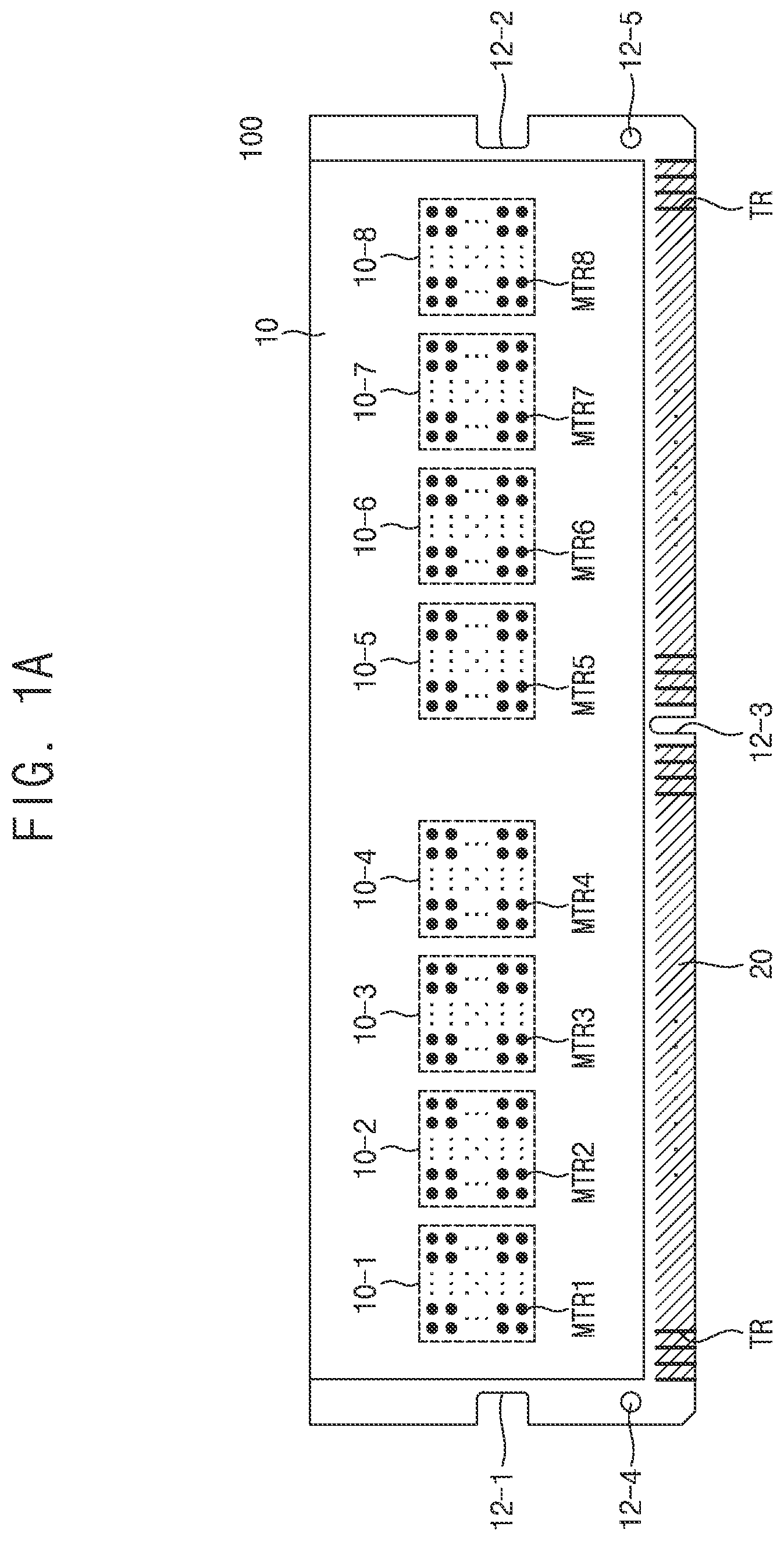
A is a diagram showing a module board according to an embodiment. A module board 100 may include a component region 10 including a predetermined number of memory regions 10 - 1 to 10 - 4 (in which a predetermined number of (e.g., four) semiconductor memory devices are installed) which are arranged to from a left portion to a central portion of at least one (e.g., an upper surface) of an upper surface or a lower surface of the module board 100 and a predetermined number of memory regions 10 - 5 to 10 - 8 (in which a predetermined number of semiconductor memory devices are installed) which are arranged from the central portion to a right portion of at least one of an upper surface and a lower surface of the module board 100 . A terminal (e.g., a tab) region 20 may be disposed in an edge region of one side (e.g., a lower side) of one surface of the module board 100 , and a plurality of terminals TR may be arranged in a line (in the form of a stripe) in the terminal region 20 . A plurality of module terminals MTR 1 , MTR 2 , . . . , and MTR 8 may be arranged at corresponding positions in a plurality of memory terminals (e.g., balls) of semiconductor memory devices in the memory regions 10 - 1 to 10 - 8 , respectively. However, the number of memory regions are not limited thereto, and may include any number of memory regions. The plurality of module terminals MTR 1 , MTR 2 , . . . , and MTR 8 may be terminals to which data, a command/address, a clock signal, control signals, power, and so on are applied. The plurality of terminals TR may be terminals to which data, a command/address, a clock signal, control signals, and power are communicated. The module board 100 may include notches 12 - 1 to 12 - 3 and holes 12 - 4 and 12 - 5 , which may serve as reference points for the positions of the module board 100 .
B is a cross-sectional view of the module board 100 according to an embodiment.
Referring to B , the module board 100 may be a printed circuit board configured by stacking a plurality of layers L 1 to Ln, where n is an integer greater than or equal to 1. The plurality of terminals TR may be arranged on an upper surface of the first layer L 1 and a lower surface of the n th layer Ln of the module board 100 . The plurality of memory regions 10 - 1 to 10 - 8 may be disposed on at least one of the upper surface of the first layer L 1 and the lower surface of the n th layer of the module board 100 . Signal lines (e.g., lines for transmitting data, a command/address, a clock signal, and control signals) and/or power lines may be arranged on upper surfaces and/or lower surfaces of the layers L 1 to Ln of the module board 100 . The plurality of terminals TR may be connected to signals (e.g., data, a command/address, a clock signal, and control signals) and/or power applied from an external device (e.g., a central processing unit (CPU) or a graphic processing unit (GPU)). The plurality of terminals TR may transmit the signals and/or the power to corresponding signal lines and/or power lines that are arranged on at least one layer among the other layers L 2 to Ln through corresponding vias of the first layer L 1 . The signals and/or power applied to the plurality of terminals TR may be transmitted to the plurality of module terminals MTR 1 , MTR 2 , . . . , and MTR 8 through signal lines and vias arranged on at least two layers among the n layers L 1 to Ln of the module board 100 .
is a schematic diagram showing arrangement of clock signal lines according to an embodiment. CKT refers to a clock signal terminal among the plurality of terminals TR of the module board 100 . MCKT 1 to MCKT 8 refer to module clock signal terminals of the eight module terminals MTR 1 to MTR 8 arranged in the memory regions 10 - 1 to 10 - 8 . For example, the module clock signal terminals may be referred to as MCKTk, where k is an integer greater than or equal to 1. MRTT 1 and MRTT 2 refer to a first termination resistance terminal and a second termination resistance terminal, respectively, that are arranged in the component region 10 .
Referring to , a clock signal terminal CKT may be connected to a branch point dp by a branch line dsl and may be connected to a first point p 1 from the branch point dp by a first signal line sl 1 . The first point p 1 may correspond to a point of the memory region 10 - 1 at which the module clock signal terminal MCKT 1 is disposed.
The first point p 1 may be connected to a fifth point p 5 sequentially through a second point p 2 , a third point p 3 , and a fourth point p 4 by a second signal line sl 2 . The second point p 2 , the third point p 3 , and the fourth point p 4 may correspond to points of the memory regions 10 - 2 , 10 - 3 , and 10 - 4 , respectively, at which the module clock signal terminals MCKT 2 , MCKT 3 , and MCKT 4 are arranged. The fifth point p 5 may be a point corresponding to the first termination resistance terminal MRTT 1 to which a first termination resistor is connected. A first predetermined interval d 1 may be provided between the first point p 1 and the second point p 2 , between the second point p 2 and the third point p 3 , and between the third point p 3 and the fourth point p 4 . The length of the first signal line sl 1 may be smaller than the first predetermined interval d 1 . In addition, a second predetermined interval d 2 may be provided between the first point p 1 and the first module clock signal terminal MCKT 1 , the second point p 2 and the second module clock signal terminal MCKT 2 , the third point p 3 and the third module clock signal terminal MCKT 3 , and the fourth point p 4 and the fourth module clock signal terminal MCKT 4 , and the fifth point p 5 and the first termination resistance terminal MRTT 1 . The length of the first signal line sl 1 may be greater than the second predetermined interval d 2 . However, the predetermined intervals are not limited thereto, and the first predetermined interval and the second predetermined interval may vary between the points and/or between the points and the module clock signal terminals.
The branch point dp may be connected to a sixth point p 6 by a third signal line sl 3 . The sixth point p 6 may correspond to a point of the memory region 10 - 5 at which the module clock signal terminal MCKT 5 is disposed. The length of the third signal line sl 3 may be greater than the sum of the length of the first signal line sl 1 and the length of the second signal line sl 2 . However, the lengths of the signal lines are not limited thereto, and the lengths of the signal lines may be variously configured.
The sixth point p 6 may be connected to a tenth point p 10 sequentially through a seventh point p 7 , an eighth point p 8 , and a ninth point p 9 by a fourth signal line sl 4 . The length of the fourth signal line sl 4 may be equal to the length of the second signal line sl 2 . The seventh point p 7 , the eighth point p 8 , and the ninth point p 9 may correspond to points of the memory regions 10 - 6 , 10 - 7 , and 10 - 8 , respectively, at which the module clock signal terminals MCKT 6 , MCKT 7 , and MCKT 8 are arranged, and the tenth point p 10 may be a point at which the second termination resistance terminal MRTT 2 is disposed. The first predetermined interval d 1 may be provided between the sixth point p 6 and the seventh point p 7 , between the seventh point p 7 and the eighth point p 8 , and between the eighth point p 8 and the ninth point p 9 . In addition, the second predetermined interval d 2 may be provided between the sixth point p 6 and the fifth module clock signal terminal MCKT 5 , the seventh point p 7 and the sixth module clock signal terminal MCKT 6 , the eighth point p 8 and the seventh module clock signal terminal MCKT 7 , the ninth point p 9 and the eighth module clock signal terminal MCKT 8 , and the tenth point p 10 and the second termination resistance terminal MRTT 2 .
is a diagram showing arrangement of clock signal lines according to an embodiment. illustrates an example in which the arrangement of the clock signal lines shown in is embodied on the module board 100 and illustrates an example of the case in which the clock signal terminal CKT is disposed at a central portion of the terminal region 20 .
Referring to , the clock signal terminal CKT disposed on an upper surface of a first layer L 1 of the module board 100 and a via v 11 may be connected by a first sub branch line dsl 1 . The via v 11 may be connected to a via v 21 of a second layer L 2 , and the via v 21 may be connected to a via v 22 disposed adjacent to a clock signal via vck 21 of the second layer L 2 corresponding to the module clock signal terminal MCKT 1 by a second sub branch line dsl 2 . The via v 22 may be connected to a via v 32 of a third layer L 3 . The first sub branch line dsl 1 and the second sub branch line dsl 2 may correspond to the branch line dsl of .
The via v 32 of the third layer L 3 may be connected to a clock signal via vck 31 of the third layer L 3 corresponding to the module clock signal terminal MCKT 1 by the first signal line sl 1 , and the clock signal vias vck 31 , vck 32 , vck 33 , and vck 34 of the third layer L 3 corresponding to the module clock signal terminals MCKT 1 , MCKT 2 , MCKT 3 , and MCKT 4 and the via v 33 of the third layer L 3 corresponding to the first termination resistance terminal MRTT 1 may be connected to each other by the second signal line sl 2 . The via v 32 of the third layer L 3 may be connected to a clock signal via vck 35 of the third layer L 3 corresponding to the module clock signal terminal MCKT 5 by the third signal line sl 3 , and clock signal vias vck 35 , vck 36 , vck 37 , and vck 38 of the third layer L 3 corresponding to the module clock signal terminals MCKT 5 , MCKT 6 , MCKT 7 , and MCKT 8 and a via v 34 of the third layer L 3 corresponding to the second termination resistance terminal MRTT 2 may be connected to each other by the fourth signal line sl 4 .
The module clock signal terminals MCKT 1 to MCKT 4 , the first termination resistance terminal MRTT 1 , the module clock signal terminals MCKT 5 to MCKT 8 , and the second termination resistance terminal MRTT 2 , which are arranged on the first layer L 1 , may be connected to clock signal vias vck 21 to vck 24 , a via v 23 , clock signal vias vck 25 to vck 28 , and a via v 24 , which are arranged on the second layer L 2 , through clock signal vias vck 11 to vck 14 , a via v 13 , clock signal vias vck 15 to vck 18 , and a via v 14 , which are arranged on the first layer L 1 , and may also be connected to clock signal vias vck 31 to vck 34 , a via v 33 , clock signal vias vck 35 to vck 38 , and a via v 34 , which are arranged on the third layer L 3 . In , the module clock signal terminals MCKT 1 to MCKT 4 , the first termination resistance terminal MRTT 1 , the module clock signal terminals MCKT 5 to MCKT 8 , and the second termination resistance terminal MRTT 2 , and the clock signal vias vck 11 to vck 14 , the via v 13 , the clock signal vias vck 15 to vck 18 , and the via v 14 , which are connected thereto, are integrally illustrated. In addition, connections between vertically connected vias are illustrated as dotted lines, and each of the dotted lines may correspond to the second predetermined interval d 2 shown in .
Although illustrates an example in which the first signal line sl 1 to the fourth signal line sl 4 are arranged on the third layer L 3 , the one or more embodiments are not limited thereto, and the first signal line sl 1 to the fourth signal line sl 4 may be arranged on the second layer L 2 . In addition, the first signal line sl 1 and/or the fourth signal line sl 4 may also be distributed and arranged on at least two layers, not on a single layer. The first signal line sl 1 to the fourth signal line sl 4 may be arranged on at least one of the n layers L 1 to Ln.
The arrangement of the clock signal lines described above with reference to may have an asymmetric Y-topology structure. According to this structure, large signal attenuation occurs at the first point p 1 and the sixth point p 6 due to a difference between the length of the first signal line sl 1 to the first point p 1 from the branch point dp and the length of the third signal line sl 3 to the sixth point p 6 from the branch point dp. The signal attenuation may be reduced when the first predetermined interval d 1 between the first to fourth points p 1 to p 4 and between the sixth to ninth points p 6 to p 9 is short. That is, the length of the second signal line sl 2 to the fifth point p 5 from the first point p 1 at which signal attenuation begins to occur and the length of the fourth signal line sl 4 to the tenth point p 10 from the sixth point p 6 at which signal attenuation begins to occur may be configured to be shorter.
For example, the command/address lines may also be arranged with the asymmetric Y-topology structure.
is a conceptual diagram showing arrangement of command/address lines according to an embodiment. A command/address terminal (CAT) may be a terminal among a plurality of terminals TR of the module board 100 . MCAT 1 to MCAT 8 may refer to module command/address terminals among the eight module terminals MTR 1 to MTR 8 arranged in the memory regions 10 - 1 to 10 - 8 .
Referring to , the command/address terminal CAT and an eleventh point p 11 may be connected to each other by a fifth signal line sl 5 . The fifth signal line sl 5 may have a length that is a sum of the length of the branch line dsl and the length of the first signal line sl 1 shown in in order to match timing between a clock signal applied through the clock signal terminal CKT and a command/address applied through the command/address terminal CAT. The eleventh point p 11 may correspond to a point of the memory region 10 - 1 at which the module command/address terminal MCAT 1 is disposed. The eleventh point p 11 to a nineteenth point p 19 may be connected by a sixth signal line sl 6 . A twelfth point p 12 to an eighteenth point p 18 may correspond to points of the memory regions 10 - 2 to 10 - 8 at which the module command/address terminals MCAT 2 to MCAT 8 are arranged, and the nineteenth point p 19 may correspond to a point at which a third termination resistance terminal MRTT 3 is disposed. A distance between a fourteenth point p 14 and a fifteenth point p 15 may be a third predetermined interval d 3 that is greater than the first predetermined interval d 1 .
is a diagram showing arrangement of command/address lines according to an embodiment. illustrates an example in which the arrangement of the command/address lines shown in is embodied on the module board 100 and illustrates an example in which the command/address terminal CAT is disposed at a central portion of the terminal region 20 .
Referring to , the command/address terminal CAT disposed on an upper surface of the first layer L 1 of the module board 100 and a via v 15 may be connected by a first sub signal line sl 51 . The via v 15 may be connected to a via v 25 of the second layer L 2 , and the via v 25 may be connected to a command/address via vca 21 of the second layer L 2 corresponding to the module command/address terminal MCAT 1 by a second sub signal line sl 52 . The first sub signal line sl 51 and the second sub signal line sl 52 may correspond to the fifth signal line sl 5 shown in . The sum of the length of the first sub signal line sl 51 and the length of the second sub signal line sl 52 may be equal to the sum of the length of the first sub signal line sl 51 , the length of the second sub signal line sl 52 , and the length of the first signal line sl 1 shown in .
The module command/address terminals MCAT 1 to MCAT 8 , and the third termination resistance terminal MRTT 3 , which are arranged on the first layer L 1 , may be connected to command/address vias vca 21 to vca 28 , and a via v 26 arranged on the second layer L 2 through command/address vias vca 11 to vca 18 , and a via v 16 , which are arranged on the first layer L 1 . In , the module command/address terminals MCAT 1 to MCAT 8 , and the third termination resistance terminal MRTT 3 , and the command/address vias vca 11 to vca 18 , and the via v 16 , which are connected thereto, are integrally illustrated. Here, connections between vertically connected vias are illustrated as dotted lines, and each of the dotted lines may correspond to the second predetermined interval d 2 shown in .
The arrangement of the command/address lines described above with reference to may have a fly-by topology structure.
Although illustrates an example in which the fifth signal line sl 5 and the sixth signal line sl 6 are arranged on the second layer L 2 , the fifth signal line sl 5 and the sixth signal line sl 6 may be arranged on the other layers, for example, layers L 3 to Ln. In addition, the fifth signal line sl 5 and/or the sixth signal line sl 6 may also be distributed and arranged on at least two different layers, not on a single layer. The fifth signal line sl 5 and the sixth signal line sl 6 may be arranged on at least one of the n layers L 1 to Ln.
is a conceptual diagram showing arrangement of command/address lines according to an embodiment. CAT refers to one command/address terminal among a plurality of terminals TR of the module board 100 and MCAT 1 to MCAT 8 refer to the module command/address terminals among the eight module terminals MTR 1 to MTR 8 arranged in the memory regions 10 - 1 to 10 - 8 .
Referring to , the command/address terminal CAT may be connected to a branch point dp′ by a branch line dsl′ and may be connected to the eleventh point p 11 from the branch point dp′ by a seventh signal line sl 7 . The eleventh point p 11 may correspond to a point of the memory region 10 - 1 at which the module command/address terminal MCAT 1 is disposed. The sum of the length of a branch line dsl′ and the length of a seventh signal line sl 7 may be equal to the sum of the length of the branch line dsl and the length of the first signal line sl 1 shown in in order to match timing between a clock signal applied through the clock signal terminal CKT and a command/address applied through the command/address terminal CAT. The eleventh point p 11 may be connected to a twentieth point p 20 sequentially through a thirteenth point p 13 , the fifteenth point p 15 , and a seventeenth point p 17 by an eighth signal line sl 8 . The thirteenth point p 13 , the fifteenth point p 15 , and the seventeenth point p 17 may correspond to points of the memory regions 10 - 3 , 10 - 5 , and 10 - 7 , respectively, at which the module command/address terminals MCAT 3 , MCAT 5 , and MCAT 7 are arranged, and the twentieth point p 20 may correspond to points at which a fourth termination resistance terminal MRTT 4 is disposed. A fourth predetermined interval d 4 may be provided between the eleventh point p 11 and the thirteenth point p 13 , and between the fifteenth point p 15 and the seventeenth point p 17 . The fourth predetermined interval d 4 may have a length that is twice the first predetermined interval d 1 (e.g., d 4 =2×d 1 ).
The branch point dp′ may be connected to the twelfth point p 12 by a ninth signal line sl 9 . The twelfth point p 12 may correspond to a point of the memory region 10 - 2 at which the module command/address terminal MCAT 2 is disposed. The length of the ninth signal line sl 9 may be equal to the length of the seventh signal line sl 7 .
The twelfth point p 12 may be connected to the nineteenth point p 19 sequentially through the fourteenth point p 14 , a sixteenth point p 16 , and the eighteenth point p 18 by a tenth signal line sl 10 . The fourteenth point p 14 , the sixteenth point p 16 , and the eighteenth point p 18 may correspond to points of the memory regions 10 - 4 , 10 - 6 , and 10 - 8 , respectively, at which the module command/address terminals MCAT 4 , MCAT 6 , and MCAT 8 are arranged, and the nineteenth point p 19 may correspond to a point at which the third termination resistance terminal MRTT 3 is disposed. The fourth predetermined interval (e.g., d 4 =2×d 1 ) may be provided between the twelfth point p 12 and the fourteenth point p 14 , and between the sixteenth point p 16 and the eighteenth point p 18 . The length of the tenth signal line sl 10 may be equal to the length of the eighth signal line sl 8 .
is a diagram showing arrangement of command/address lines according to an embodiment. illustrates an example in which the arrangement of the command/address lines shown in is embodied on the module board 100 and illustrates an example in which the command/address terminal CAT is disposed at a central portion of the terminal region 20 .
Referring to , the command/address terminal CAT disposed on an upper surface of the first layer L 1 of the module board 100 and the via v 15 may be connected by a third sub branch line dsl 3 .
The via v 15 may be connected to the via v 25 of the second layer L 2 , and the via v 25 may be connected to the via v 26 of the second layer L 2 by a fourth sub branch line dsl 4 . The third sub branch line dsl 3 and the fourth sub branch line dsl 4 may correspond to the branch line dsl′ shown in . The via v 26 may be connected to the command/address via vca 21 disposed on the second layer L 2 by the seventh signal line sl 7 . The command/address vias vca 21 , vca 23 , vca 25 , and vca 27 , and the via v 25 may be connected to each other by the eighth signal line sl 8 . The command/address vias vca 21 , vca 23 , vca 25 , and vca 27 may be arranged at positions corresponding to the positions of the first layer L 1 at which the module command/address terminals MCAT 1 , MCAT 3 , MCAT 5 , and MCAT 7 are arranged, respectively, and the via v 25 may be disposed at a position corresponding to the position of the first layer L 1 at which the fourth termination resistance terminal MRTT 4 is disposed.
The via v 26 may be connected to a via v 36 of the third layer L 3 , and the via v 36 may be connected to a command/address via vca 32 disposed on the third layer L 3 by the ninth signal line sl 9 . Command/address vias vca 32 , vca 34 , vca 36 , and vca 38 and a via v 37 may be connected to each other by the tenth signal line sl 10 . The command/address vias vca 32 , vca 34 , vca 36 , and vca 38 may be arranged at positions of the first layer L 1 at which the module command/address terminals MCAT 2 , MCAT 4 , MCAT 6 , and MCAT 8 are arranged, respectively, and the via v 37 may be arranged at a position corresponding to the position of the first layer L 1 at which the third termination resistance terminal MRTT 3 is disposed.
The module command/address terminals MCAT 1 to MCAT 8 , and the third termination resistance terminal MRTT 3 , which are arranged on the first layer L 1 , may be connected to the command/address vias vca 21 to vca 28 , and vias v 25 and v 27 , which are arranged on the second layer L 2 , through the command/address vias vca 11 to vca 18 , and vias v 15 and v 17 , which are arranged on the first layer L 1 . In , the module command/address terminals MCAT 1 to MCAT 8 , and the third termination resistance terminal MRTT 3 , the command/address vias vca 11 to vca 18 , and the vias v 15 and v 17 , which are connected thereto, are integrally illustrated. The connections between vertically connected vias are illustrated as dotted lines, and each of the dotted lines may correspond to the second predetermined interval d 2 shown in .
The arrangement of the command/address lines described above with reference to may have a symmetric Y-topology structure.
Although illustrates an example in which the seventh signal line sl 7 and the eighth signal line sl 8 are arranged on the second layer L 2 and the ninth signal line sl 9 and the tenth signal line sl 10 are arranged on the third layer L 3 , the seventh signal line sl 7 and the eighth signal line sl 8 , and the ninth signal line sl 9 and the tenth signal line sl 10 may be arranged on two different layers of the other layers L 3 to Ln. In another embodiment, the seventh to tenth signal lines sl 7 to sl 10 may also be arranged on the second layer L 2 or the third layer L 3 . That is, the seventh to tenth signal lines sl 7 to sl 10 may also be arranged on at least one of the second to n th layers L 2 to Ln. The seventh signal line sl 7 to the tenth signal line sl 10 may also be distributed and arranged on at least three layers.
The arrangement of the command/address lines according to an embodiment may have one of an asymmetric Y-topology structure, a fly-by topology structure, and a symmetric Y-topology structure.
According to one or more embodiments, the clock signal line and the command/address line may be arranged on the same layer as long as they do not overlap with each other. However, when the clock signal line and the command/address line need to be arranged such that they need to overlap each other, the clock signal line and the command/address line may be provided on different layers.
is a diagram showing the configuration of a memory module according to an embodiment. A memory module 200 may include the module board 100 , a plurality of (e.g., 8) semiconductor memory devices M 1 to M 8 , and first to third termination resistors RTT 1 to RTT 3 . The terminals of the memory module 200 may include the clock signal terminal CKT, the command/address terminals CAT, and the plurality of (e.g., first to eighth) data terminals DQT 1 to DQT 8 (as shown in ).
Referring to , the memory module 200 may commonly apply a clock signal CK through the clock signal terminal CKT to the semiconductor memory devices M 1 to M 8 . The arrangement of the clock signal lines may have the aforementioned asymmetric Y-topology structure. The memory module 200 may commonly apply a command/address CA through the command/address terminals CAT to the semiconductor memory devices M 1 to M 8 . Also, the arrangement of the command/address lines may have the fly-by topology structure described with reference to . The memory module 200 may have control signal lines for commonly applying control signals CON through control signal terminals to the semiconductor memory devices M 1 to M 8 , and the arrangement of the control signal lines may be the same as the arrangement of the command/address lines. Each of the plurality of semiconductor memory devices M 1 to M 8 may be a memory device having large load or capacity. Examples of the device may include a double data rate (DDR) (e.g., DDR3, DDR4, or DDR5) semiconductor memory device, a dual-die package (DDP) semiconductor memory device, or a high bandwidth memory (HBM) device. The memory module 200 may be an unbuffered dual in-line memory module, which does not include a buffer, or a small outline dual in-line memory module (SODIMM).
The memory module 200 may transmit first data DQ 1 to eighth data DQ 8 applied through the first data terminal DQT 1 to the eighth data terminal DQT 8 to the semiconductor memory devices M 1 to M 8 , respectively, or may transmit the first data DQ 1 to the eighth data DQ 8 output from the semiconductor memory devices M 1 to M 8 to the first data terminal DQT 1 to eighth data terminal DQT 8 , respectively. Each of the first data DQ 1 to the eighth data DQ 8 may be predetermined-bit (e.g., 4, 8, or 16 bits) data.
When the arrangement of the command/address line has an asymmetric Y-topology structure or a symmetric Y-topology structure, the memory module 200 may include a third termination resistor and a fourth termination resistor.
is a diagram showing a semiconductor memory device according to an embodiment. A semiconductor memory device 300 may be a DDP semiconductor memory device.
Referring to , the DDP semiconductor memory device 300 may include a package substrate PSUB, a first die D 1 , and a second die D 2 . The first die D 1 and the second die D 2 may be sequentially stacked on the package substrate PSUB. The package substrate PSUB may include upper pads UPAD arranged on an upper surface of the package substrate PSUB, lower pads LPAD arranged on a lower surface of the package substrate PSUB, and signal lines for connecting pads corresponding to the upper pads UPAD and the lower pads LPAD. The DDP semiconductor memory device 300 may include memory terminals B (e.g., balls) attached to the lower pads LPAD.
A first redistribution layer RDL 1 may be disposed on an upper surface of the first die D 1 , and a second redistribution layer RDL 2 may be disposed on an upper surface of the second die D 2 . The first redistribution layer RDL 1 may redistribute the positions of pads (not shown) of the first die D 1 . For example, the pads (not shown) of the first die D 1 , disposed at a central portion of the first die D 1 , may be connected to pads RDL 1 P of the first redistribution layer RDL 1 , disposed at an edge portion of the upper surface of the first redistribution layer RDL 1 , through the first redistribution layer RDL 1 . The second redistribution layer RDL 2 may redistribute the positions of the pads (not shown) of the second die D 2 . For example, the pads (not shown) of the second die D 2 , disposed at a central portion of the second die D 2 , may be connected to pads RDL 2 P of the second redistribution layer RDL 2 , disposed at an edge portion of the upper surface of the second redistribution layer RDL 2 , through the second redistribution layer RDL 2 . The upper pads UPAD and corresponding pads among the pads RDL 1 P may be wire-bonded to each other by wires WB, and the upper pads UPAD and corresponding pads among the pads RDL 2 P may be wire-bonded to each other by wires WB. In addition, the DDP semiconductor memory device 300 may include an encapsulant ENC for encapsulating the package substrate PSUB, the first die D 1 , and the second die D 2 .
is a diagram showing the configuration of a semiconductor memory device according to an embodiment. illustrates connection between memory terminals B, and the first die D 1 and the second die D 2 shown in .
Referring to , the memory terminals B may include first memory control signal terminal BCON 1 , a second memory control signal terminal BCON 2 , a memory clock signal terminal BCK, a memory command/address terminal BCA, and a memory data terminal BDQ. Here, one representative terminal for each signal is illustrated.
The first memory control signal terminals BCON 1 including a first memory chip selection signal terminal BCS 1 , a first memory clock enable signal terminal BCKE 1 , and a first memory on-die termination signal terminal BODT 1 may be connected to the first die D 1 . The second memory control signal terminals BCON 2 including a second memory chip selection signal terminal BCS 2 , a second memory clock enable signal terminal BCKE 2 , and a second memory on-die termination signal terminal BODT 2 may be connected to the second die D 2 . The memory clock signal terminal BCK, the memory command/address terminal BCA, and the memory data terminal BDQ may be commonly connected to the first die D 1 and the second die D 2 .
With reference to , an operation of the first die D 1 and the second die D 2 will be described below.
The first die D 1 may be selected in response to a first chip selection signal CS 1 , a first clock enable signal CKE 1 , and a first on-die termination signal ODT 1 being applied to respective terminals of the first memory control signal terminals BCON 1 . When the first die D 1 is selected, data DQ may be input or output in response to the clock signal CK and the command/address.
The second die D 2 may be selected in response to a second chip selection signal CS 2 , a second clock enable signal CKE 2 , and a second on-die termination signal ODT 2 being applied to respective terminals of the second memory control signal terminals BCON 2 . When the second die D 2 is selected, the data DQ may be input or output in response to the clock signal CK and the command/address.
For example, each of the first die D 1 and the second die D 2 shown in may be a DDR (e.g., DDR4) semiconductor memory device.
Although not shown, the arrangement of control signal lines may have one structure from among an asymmetric Y-topology structure, a fly-by topology structure, and a symmetric Y-topology structure, like the arrangement of the command/address lines.
is a diagram showing a memory system according to an embodiment. A memory system 1000 may include at least one memory module 200 and a control unit 400 .
In , the memory module 200 may be the module board 100 described above with reference to A to 7 and the memory module described above with reference to to 10 . In , data terminals of the terminals TR of A are denoted by DQT, command/address terminals are denoted by CAT, a clock signal terminal is denoted by CKT, and control signal terminals are denoted by CONT.
The control unit 400 may be, for example, a central processing unit (CPU) or a graphic processing unit (GPU). The control unit 400 may transmit a first plural-bits command/address, control signals CA, and a clock signal CK. The control unit 400 may transmit and receive eight pieces of second plural-bits data DQ 1 to DQ 8 .
is a block diagram showing the configuration of a control device according to an embodiment. The control device 400 may include a processor 400 - 2 , a command/address and control signal generator 400 - 4 , a clock signal generator 400 - 6 , and a data input and output unit 400 - 8 .
The function of each of blocks shown in will be described below.
The processor 400 - 2 may generate a command COM, an address ADD, and a control signal con by executing a program according to an external command ECOM and may transmit and receive data DATA. For example, the processor 400 - 2 may receive the external command ECOM by communicating with various input devices, for example, a keyboard, a mouse, a touch sensor, a sound sensor, a fingerprint sensor, or a motion recognition sensor, and may generate the command COM, the address ADD, an internal control signal CONT, and data DATA by executing a program according to the external command ECOM. The processor 400 - 2 may receive and process the data DATA, and may output the data DATA to various output devices, for example, a display unit or a sound output unit. The processor 400 - 2 may additionally generate a clock signal control signal ckcon and transmit the clock signal control signal ckcon to a clock signal generator 400 - 6 .
The command/address and control signal generator 400 - 4 may receive the command COM and the address ADD in response to an internal clock signal CK received from the clock signal generator 400 - 6 , to generate the command/address CA of a first predetermined bit. The command/address and control signal generator 400 - 4 may also generate the control signal CON in response to the internal control signal con.
The clock signal generator 400 - 6 may generate the internal clock signal CK and the clock signal CK in response to the clock signal control signal ckcon received from the processor 400 - 2 .
The data input and output unit 400 - 8 may receive the data DATA in response to the internal clock signal CK to generate eight pieces of the data DQ 1 to DQ 8 of a second predetermined bit or may receive the eight pieces of the data DQ 1 to DQ 8 of a second predetermined bit to generate the data DATA. For example, the data input and output unit 400 - 8 may generate the eight pieces of the data DQ 1 to DQ 8 of a second predetermined bit in response to the internal clock signal CK according to a DDR protocol.
According to the one or more embodiments of the present disclosure, the clock signal lines and/or the command/address lines of the module board may be arranged in the form of an asymmetric Y-topology structure, and thus even if the number of the plurality of semiconductor memory devices installed on the module board is large, the quality of the clock signal and the command/address may not be affected. Thus, the reliability of the operation of the memory module and the memory system may be improved.
While the one or more embodiments of the disclosure have been described with reference to the accompanying drawings, it will be understood by those skilled in the art that various modifications may be made without departing from the scope of the inventive concept and without changing essential features thereof. Therefore, the above-described embodiments are only example embodiment, and should be considered in a descriptive sense only and not for the purposes of limitation.
Figures (12)
Citations
This patent cites (30)
- US7155627
- US7606042
- US7746095
- US7869243
- US8036011
- US9082464
- US9449650
- US9524756
- US9558806
- US9704559
- US9786354
- US9793034
- US9811265
- US9980366
- US10199363
- US10622029
- US20040105292
- US20060184756
- US20080030966
- US20090027940
- US20090243649
- US20100125693
- US20120250264
- US20140233335
- US20160205767
- US20180165243
- US20190304565
- US20200042492
- US20210407565
- US201942910