Wireless Signal Transceiver Device with a Dual-polarized Antenna with at Least Two Feed Zones
Abstract
A transceiver includes an antenna configured to transmit a first wireless signal based on a transmission signal and receive a second wireless signal, the second wireless signal including a reflected first wireless signal from an object and the antenna transmitting the first wireless signal and receiving the second wireless signal at the same time. A transmission circuit is configured to generate the transmission signal and output the transmission signal to a first side of the antenna. A reception circuit is configured to receive a reception signal from a second side of the antenna, the antenna outputting the reception signal based on the second wireless signal. The first side is different from the second side.
Claims (14)
1. A transceiver, comprising: an antenna configured to: transmit a first wireless signal based on a transmission signal; and receive a second wireless signal, the second wireless signal comprising a reflected first wireless signal from an object, the antenna transmitting the first wireless signal and receiving the second wireless signal at the same time; a transmission circuit configured to generate the transmission signal and output the transmission signal to a first side of the antenna; and a reception circuit configured to receive a reception signal from a second side of the antenna, the antenna outputting the reception signal based on the second wireless signal; wherein the first side is different from the second side.
11. A transceiver, comprising: an antenna configured to: transmit a first wireless signal based on a transmission signal; and receive a second wireless signal, the second wireless signal comprising a reflected first wireless signal from an object, the antenna transmitting the first wireless signal and receiving the second wireless signal at the same time; a transmission circuit configured to generate the transmission signal and output the transmission signal to a first feed point for the antenna; and a reception circuit configured to receive a reception signal from a second feed point for the antenna, the antenna outputting the reception signal based on the second wireless signal; wherein: a first direction is defined from the first feed point to a centroid of the antenna; a second direction is defined from the second feed point to the centroid of the antenna; and the first and second directions are orthogonal or form an acute angle not less than 45 degrees.
Show 12 dependent claims
2. The transceiver of claim 1 , wherein: a first direction is defined from a midpoint of the first side to a centroid of the antenna; a second direction is defined from a midpoint of the second side to the centroid of the antenna; and the first direction is orthogonal to the second direction.
3. The transceiver of claim 1 , wherein the first side and the second side are adjacent sides of the antenna.
4. The transceiver of claim 1 , wherein the first side is orthogonal to the second side.
5. The transceiver of claim 1 , wherein: the transmission circuit is configured to output the transmission signal to a first feed point on the first side of the antenna; and the reception circuit is configured to receive the reception signal from a second feed point on the second side of the antenna.
6. The transceiver of claim 5 , wherein: a first direction is defined from the first feed point to a centroid of the antenna; a second direction is defined from the second feed point to the centroid of the antenna; and the first direction is orthogonal to the second direction.
7. The transceiver of claim 5 , wherein: the first side comprises a first U-shaped portion, wherein the first feed point is on the first U-shaped portion; and the second side comprises a second U-shaped portion, wherein the second feed point is on the second U-shaped portion.
8. The transceiver of claim 1 , further comprising: a first feed element corresponding to the first side; and a second feed element corresponding to the second side; wherein: the transmission circuit is configured to output the transmission signal to the first feed element; the first feed element is configured to feed the transmission signal to the first side of the antenna through electromagnetic induction; the second feed element is configured to be fed the reception signal from the second side of the antenna; and the reception circuit is configured to receive the reception signal from the second feed element.
9. The transceiver of claim 8 , wherein: the first side comprises a first U-shaped portion; the second side comprises a second U-shaped portion; the first feed element is configured to feed the transmission signal to the first U-shaped portion of the first side through electromagnetic induction; and the second feed element is configured to be fed the reception signal from the second U-shaped portion of the second side.
10. The transceiver of claim 1 , wherein the antenna comprises a dual-polarized antenna.
12. The transceiver of claim 11 , wherein: the first feed point is on the antenna; and the second feed point is on the antenna.
13. The transceiver of claim 11 , further comprising: a first feed element comprising the first feed point and configured to feed the transmission signal to the antenna through electromagnetic induction; and a second feed element comprising the second feed point and configured to be fed the reception signal from the antenna through electromagnetic induction.
14. The transceiver of claim 11 , wherein the antenna comprises a dual-polarized antenna.
Full Description
Show full text →
CROSS-REFERENCE TO RELATED APPLICATION
This application is a continuation-in-part of U.S. application Ser. No. 17/037,657, filed Sep. 29, 2020, claiming the benefit of U.S. Provisional Application No. 63/006,064 filed on Apr. 6, 2020, and being a continuation-in-part of U.S. application Ser. No. 16/698,867, filed Nov. 27, 2019, issued as U.S. Pat. No. 10,833,745, and being a continuation-in-part of U.S. application Ser. No. 16/157,106, filed Oct. 11, 2018, issued as U.S. Pat. No. 10,530,413, and claiming the priority to Taiwan Application No. 107105524 filed on Feb. 14, 2018, and the benefit of U.S. Provisional Application No. 62/607,922 filed on Dec. 20, 2017. The entire contents of all the above applications are hereby incorporated by reference.
TECHNICAL FIELD
The invention is related to a wireless signal transceiver device, and more particularly, a wireless signal transceiver device including a dual-polarized antenna with at least two feed zones.
BACKGROUND
In the field of wireless communications, dual-polarized antennas are used to perform both wireless signal reception and transmission. To perform transmitting and receiving functions of a dual-polarized antenna, a wireless communication device system may receive an external wireless signal using a reception antenna and transmit a wireless signal to an external environment using a transmission antenna. Although the wireless communication device can transmit and receive the wireless signals using the transmission and reception antennas, respectively, the two antennas require more space in the wireless communication device and may increase the overall size.
SUMMARY
Embodiments of the present disclosure provide transceiver devices including a dual-polarized antenna with at least two feed zones.
These embodiments include a transceiver including an antenna configured to transmit a first wireless signal based on a transmission signal and receive a second wireless signal, the second wireless signal including a reflected first wireless signal from an object; a transmission circuit configured to generate the transmission signal and output the transmission signal to a first side of the antenna; and a reception circuit configured to receive a reception signal from a second side of the antenna, the antenna outputting the reception signal based on the second wireless signal; wherein the first side is different from the second side.
These embodiments also include a transceiver including an antenna configured to transmit a first wireless signal based on a transmission signal and receive a second wireless signal, the second wireless signal including a reflected first wireless signal from an object; a transmission circuit configured to generate the transmission signal and output the transmission signal to a first feed point for the antenna; and a reception circuit configured to receive a reception signal from a second feed point for the antenna, the antenna outputting the reception signal based on the second wireless signal; wherein a first direction is defined from the first feed point to a centroid of the antenna, a second direction is defined from the second feed point to the centroid of the antenna, and the first and second directions are orthogonal or form an acute angle not less than 45 degrees.
It is to be understood that the foregoing general description and the following detailed description are exemplary and explanatory only, and are not restrictive of the invention, as claimed.
BRIEF DESCRIPTION OF THE DRAWINGS
illustrates a wireless signal transceiver device according to an embodiment.
illustrates a wireless signal transceiver device according to another embodiment.
illustrates a wireless signal transceiver device according to another embodiment.
illustrates a wireless signal transceiver device according to another embodiment.
illustrates a wireless signal transceiver device according to another embodiment.
illustrates a wireless signal transceiver device according to another embodiment.
illustrates a wireless signal transceiver device according to another embodiment.
illustrates a wireless signal transceiver device according to another embodiment.
illustrates a wireless signal transceiver device according to another embodiment.
illustrates a wireless signal transceiver device according to another embodiment.
illustrates a portion of a wireless signal transceiver device according to an embodiment.
illustrates a portion of a wireless signal transceiver device according to an embodiment.
illustrates a wireless signal transceiver device according to another embodiment.
illustrates a portion of wireless signal transceiver device according to another embodiment.
is a diagram of the angle versus the isolation between the wireless signals transmitted and received by the dual-polarized antenna in .
illustrates a wireless signal transceiver device according to an embodiment.
and respectively illustrate a top view and a side view of the dual-polarized antenna of .
and respectively illustrate a top view and a side view of the dual-polarized antenna according to another embodiment.
and respectively illustrate a top view and a side view of the dual-polarized antenna according to another embodiment.
and respectively illustrate a top view and a side view of the dual-polarized antenna according to another embodiment.
illustrates a top view of the dual-polarized antenna according to another embodiment.
illustrates a top view of the dual-polarized antenna according to another embodiment.
illustrates a top view of the dual-polarized antenna according to another embodiment.
illustrates a top view of the dual-polarized antenna according to another embodiment.
and respectively illustrate a top view and a partial side view of the dual-polarized antenna according to another embodiment.
illustrates a top view of the dual-polarized antenna according to another embodiment.
illustrates a perspective view of the dual-polarized antenna in .
and respectively illustrate a top view and a partial side view of the dual-polarized antenna according to another embodiment.
illustrates a top view of the dual-polarized antenna according to another embodiment.
illustrates a partial side view of the dual-polarized antenna in .
illustrates a top view of the dual-polarized antenna according to another embodiment.
illustrates a side view of the dual-polarized antenna in .
illustrates a top view of the dual-polarized antenna according to another embodiment.
illustrates a side view of the dual-polarized antenna according to another embodiment.
to illustrate top views of the dual-polarized antennas with hybrid structures according to other embodiments.
illustrates a top view of the dual-polarized antenna according to another embodiment.
illustrates a top view of a dual-polarized antenna and a circuit according to an embodiment.
illustrates an exemplary wireless signal transceiver device, according to some embodiments of the present disclosure.
illustrates another exemplary wireless signal transceiver device, according to some embodiments of the present disclosure.
illustrates another exemplary wireless signal transceiver device, according to some embodiments of the present disclosure.
illustrates another exemplary wireless signal transceiver device, according to some embodiments of the present disclosure.
DETAILED DESCRIPTION
Reference will now be made in detail to exemplary embodiments, examples of which are illustrated in the accompanying drawings. The following description refers to the accompanying drawings in which the same numbers in different drawings represent the same or similar elements unless otherwise represented. The implementations set forth in the following description of exemplary embodiments do not represent all implementations consistent with the invention. Instead, they are merely examples of apparatuses and methods consistent with aspects related to the invention as recited in the appended claims.
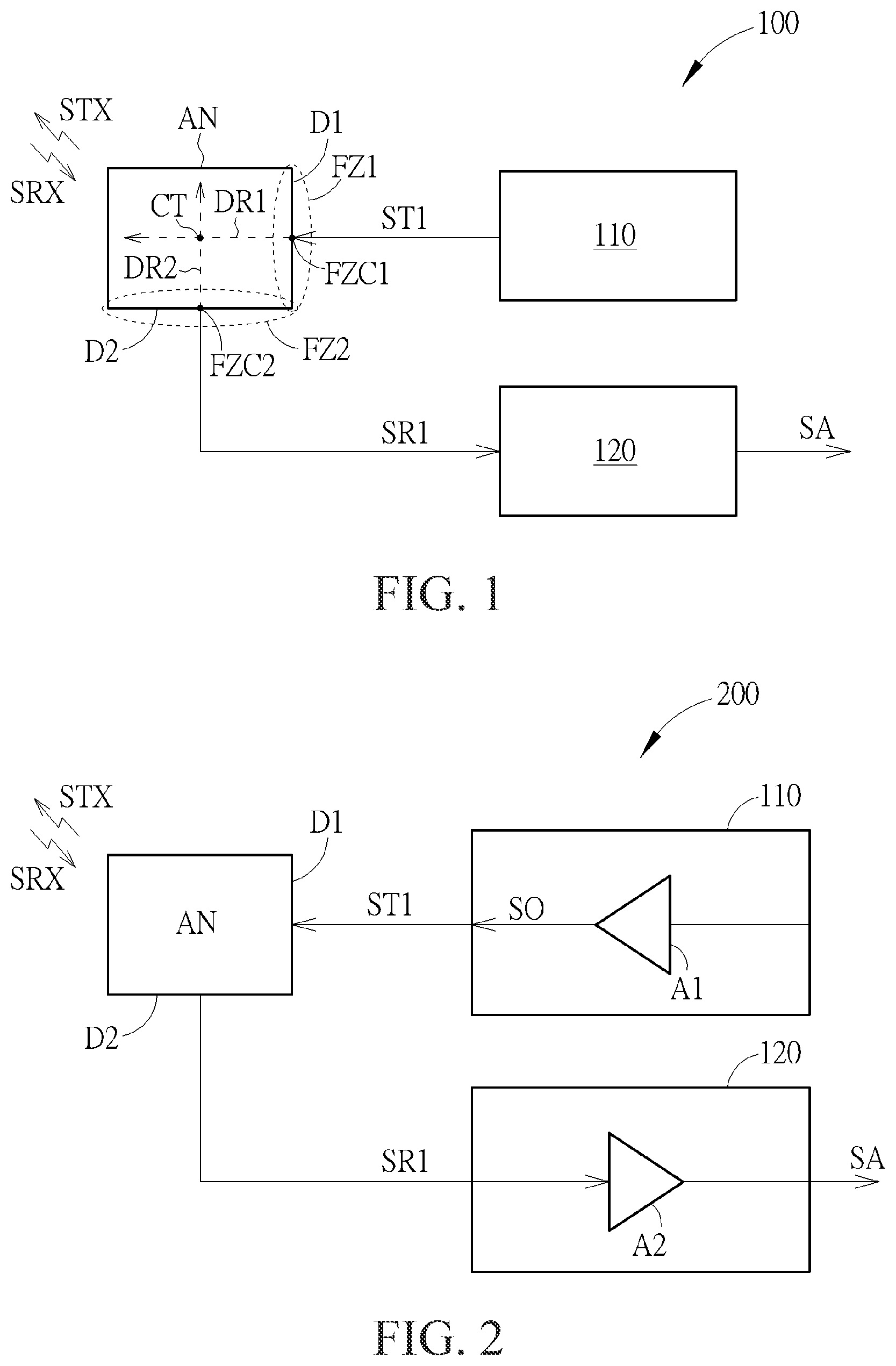
The dual-polarized antenna may have a rectangular, square, circular or oval shape. The mentioned oval shape in the text may be an elliptical shape of an accurate mathematic definition, an oval shape similar to an elliptical shape, a round shape or an oblong shape. In practice, related engineering simulations and device fine-tuning may be used to optimize the effect of transceiving signals. illustrates a wireless signal transceiver device 100 according to an embodiment. The wireless signal transceiver device 100 may include a dual-polarized antenna AN, a transmission circuit 110 and a reception circuit 120 . The dual-polarized antenna AN may be used to transmit a first wireless signal STX and receive a second wireless signal SRX substantially at the same time. The first wireless signal STX may be reflected by an object to generate the second wireless signal SRX. In an embodiment, the first wireless signal STX and the second wireless signal SRX may be radio frequency (RF) signals. During a time interval, since the first wireless signal STX is constantly reflected by an object, the second wireless signal SRX may be constantly received by the dual-polarized antenna AN, so the dual-polarized antenna AN may constantly transmit the first wireless signal STX and also receive the second wireless signal SRX substantially at the same time. In an embodiment, the waveform of the first wireless signal STX may be fixed or varied by time.
The dual-polarized antenna AN may include a feed zone FZ 1 and a feed zone FZ 2 . The dual-polarized antenna AN may have an antenna shape centroid CT. The feed zone FZ 1 may have a zone shape centroid FZC 1 , and the feed zone FZ 2 may have a zone shape centroid FZC 2 . A direction DR 1 may be defined from the zone shape centroid FZC 1 to the antenna shape centroid CT. A direction DR 2 may be defined from the zone shape centroid FZC 2 to the antenna shape centroid CT. The direction DR 1 may be substantially orthogonal to the direction DR 2 .
According to embodiments of to and , the dual-polarized antenna AN, AN 1 , AN 2 may have a rectangular shape as an example. Hence, the feed zone FZ 1 of the dual-polarized antenna AN may include a first side D 1 of the rectangle. The feed zone FZ 2 of the dual-polarized antenna AN may include a second side D 2 of the rectangle. The first side D 1 may be substantially orthogonal to the second side D 2 . The zone shape centroids FZC 1 and FZC 2 may be respectively at the middle points of the first side D 1 and the second side D 2 . According to the embodiment, the dual-polarized antenna AN may comprise a first antenna surface and a second antenna surface opposite to one another, the first antenna surface and the second antenna surface are separated by a thickness, the first antenna surface or the second antenna surface is coplanar with a reference plane. That is, the dual-polarized antenna AN may be a rectangular antenna with a thickness. However, as described above, the dual-polarized antenna AN may be not limited to a rectangular shape. In and , embodiments of dual-polarized antennas ANB with another shape are described.
In , the first side D 1 is used to receive a first transmission signal ST 1 , and the first wireless signal STX may relate to the first transmission signal ST 1 . The first side D 1 and the second side D 2 may be orthogonal to one another. According to embodiments, the first side D 1 and the second side D 2 may be adjacent to one another and have substantially the same length. The dual-polarized antenna AN may have a square shape.
According to the embodiment, a polarity of a wireless signal transmitted or received by the dual-polarized antenna AN may be orthogonal to a direction of an induced current. Hence, the first wireless signal STX and the second wireless signal SRX may hardly interfere with one another on the dual-polarized antenna AN. The length of each of the first side D 1 and the second side D 2 may be approximately half a wavelength of the first wireless signal STX or the second wireless signal SRX.
The second side D 2 may be used to transmit the first reception signal SR 1 related to the second wireless signal SRX. The transmission circuit 110 and the reception circuit 120 may be coupled to the dual-polarized antenna AN or substantially insulated from the dual-polarized antenna AN. In an embodiment, the transmission circuit 110 and the reception circuit 120 may be coupled to the dual-polarized antenna AN, the transmission circuit 110 is coupled to the first side D 1 and used to generate the first transmission signal ST 1 , and the reception circuit 120 is coupled to the second side D 2 and used to generate a processing signal SA related to the first reception signal SR 1 . According to the embodiment, the first wireless signal STX may be generated according to at least the first transmission signal ST 1 , and the first reception signal SR 1 may be generated according to the second wireless signal SRX.
illustrates a wireless signal transceiver device 200 according to another embodiment. The wireless signal transceiver device 200 may be an embodiment of the wireless signal transceiver device 100 . As shown in , the transmission circuit 110 may include a first amplifier A 1 . The first transmission signal ST 1 may be corresponding to an output signal SO outputted by the first amplifier A 1 . The reception circuit 120 may include a second amplifier A 2 , and the second amplifier A 2 may be used to amplify the first reception signal SR 1 and output the processing signal SA. According to the embodiment, the output signal SO may include a single signal or a pair of signals having a specific phase difference. The first amplifier A 1 may be a power amplifier, and the second amplifier A 2 may be a low noise amplifier (LNA).
illustrates a wireless signal transceiver device 300 according to another embodiment. The wireless signal transceiver device 300 may be an embodiment of the wireless signal transceiver device 100 . As shown in , the transmission circuit 110 may include a combiner 115 and a first amplifier A 31 . The combiner 115 may be coupled between the first side D 1 of the dual-polarized antenna AN and the first amplifier A 31 , and used to receive a first output signal SO 1 and a second output signal SO 2 outputted from the first amplifier A 31 , generate the first transmission signal ST 1 by combining the first output signal SO 1 and the second output signal SO 2 , and output the first transmission signal ST 1 to the first side D 1 . In , the first amplifier A 31 may have two output terminals for outputting the first output signal SO 1 and the second output signal SO 2 which may form a pair of differential signals.
illustrates a wireless signal transceiver device 400 according to another embodiment. The wireless signal transceiver device 400 may be an embodiment of the wireless signal transceiver device 100 . As shown in , the reception circuit 120 may include a coupler 125 and a second amplifier A 42 . The coupler 125 may be coupled between the second side D 2 of the dual-polarized antenna AN and the second amplifier A 42 , and used to receive the first reception signal SR 1 , convert the first reception signal SR 1 to a first input signal SI 1 and a second input signal SI 2 , and transmit the first input signal SI 1 and the second input signal SI 2 to the second amplifier A 42 . As shown in , the second amplifier A 42 may be used to generate the processing signal SA according to the first input signal SI 1 and the second input signal SI 2 , and the first input signal SI 1 and the second input signal SI 2 may form a pair of differential signals.
illustrates a wireless signal transceiver device 500 according to another embodiment. The wireless signal transceiver device 500 may be an embodiment of the wireless signal transceiver device 100 . The transmission circuit 110 in may include a combiner 115 and a first amplifier A 31 as shown in , and the reception circuit 120 of may include a coupler 125 and a second amplifier A 42 as shown in . The related operations are not described repeatedly.
illustrates a wireless signal transceiver device 600 according to another embodiment. In this embodiment, the transmission circuit 110 and the reception circuit 120 may be substantially insulated from the dual-polarized antenna AN. As shown in , the wireless signal transceiver device 600 may include feed elements F 1 and F 2 . Each of the feed elements F 1 and F 2 may have a T shape. For example, the feed element F 1 may have a strip conductor F 1 A and a conductive line F 1 B. Similarly, the feed element F 2 may have the two portions. The feed element F 1 may be disposed corresponding to the first side D 1 and used to receive the first transmission signal ST 1 generated by the transmission circuit 110 and feed the first transmission signal ST 1 to the dual-polarized antenna AN through electromagnetic induction. The feed element F 1 and the transmission circuit 110 may be substantially insulated from the dual-polarized antenna AN. The feed element F 2 may be disposed corresponding to the second side D 2 , and used to be fed with the first reception signal SR 1 from the dual-polarized antenna AN through electromagnetic induction and transmit the first reception signal SR 1 to the reception circuit 120 . The feed element F 2 and reception circuit 120 may be substantially insulated from the dual-polarized antenna AN.
According to embodiments, the feed element F 1 may be (but not limited to) a T shape feed element, and the strip conductor F 1 A is formed as a straight strip disposed along an edge of the dual-polarized antenna AN correspondingly. The strip conductor F 1 A and the first side D 1 of the dual-polarized antenna AN may be in parallel and be separated by a first distance L 1 . The strip conductor F 1 A may have a length 0.5 to 1 times a length of the first side D 1 . The first distance L 1 may be related to impedance corresponding to the first transmission signal ST 1 . The feed element F 1 may receive the first transmission signal ST 1 through a middle position of the strip conductor F 1 A and the conductive line F 1 B. The feed element F 2 may be (but not limited to) a T shape feed element. The strip conductor of the feed element F 2 and the second side D 2 of the dual-polarized antenna AN may be in parallel and be separated by a second distance L 2 . The strip conductor of the feed element F 2 may have a length 0.5 to 1 times a length of the second side D 2 . The second distance L 2 may be related to impedance corresponding to the first reception signal SR 1 . The feed element F 2 may transmit the first reception signal SR 1 through a middle position of the strip conductor and the conductive line of the feed element F 2 .
illustrates a wireless signal transceiver device 700 according to another embodiment. The wireless signal transceiver device 700 may include a dual-polarized antenna AN, a transmission circuit 710 and a reception circuit 720 . In addition to the first side D 1 and the second side D 2 described above, the dual-polarized antenna AN may further include a third side D 3 opposite to the first side D 1 . The third side D 3 may be substantially orthogonal to the second side D 2 , coupled to the transmission circuit 710 , and used to receive a second transmission signal ST 2 . The first wireless signal STX may be generated according to the first transmission signal ST 1 and the second transmission signal ST 2 . The transmission circuit 710 may be used to transmit the first transmission signal ST 1 and the second transmission signal ST 2 . As shown in , the dual-polarized antenna AN may further include a fourth side D 4 opposite to the second side D 2 . The fourth side D 4 may be substantially orthogonal to the first side D 1 , coupled to the reception circuit 720 , and used to transmit a second reception signal SR 2 . The first reception signal SR 1 and the second reception signal SR 2 may be generated according to the second wireless signal SRX. The reception circuit 720 may be used to receive the first reception signal SR 1 and the second reception signal SR 2 and generate the processing signal SA according to the first reception signal SR 1 and the second reception signal SR 2 . The first transmission signal ST 1 and the second transmission signal ST 2 may form a pair of differential signals. The first reception signal SR 1 and the second reception signal SR 2 may form a pair of differential signals. The relationship among the third side D 3 , the fourth side D 4 , feed zones corresponding to the sides D 3 and D 4 , and the antenna shape centroid CT may be similar to the relationship among the first side D 1 , the second side D 2 , the feed zones FZ 1 and FZ 2 , and the antenna shape centroid CT shown in , so it is not described repeatedly. However, a third direction defined from a third zone shape centroid corresponding to the third side D 3 to the antenna shape centroid CT may be opposite to the first direction DR 1 . A fourth direction defined from a fourth zone shape centroid corresponding to the fourth side D 4 to the antenna shape centroid CT may be opposite to the second direction DR 2 .
illustrates a wireless signal transceiver device 800 according to another embodiment. Similarities between and are not described repeatedly. As shown in , the wireless signal transceiver device 800 may include feed elements F 1 to F 4 . Like and , the dual-polarized antenna AN may have four feed zones FZ 1 to FZ 4 respectively including the first side D 1 to the fourth side D 4 . The feed elements F 1 and F 2 may be as described above. The third feed element F 3 may be similar to the feed element F 1 and be disposed corresponding to the third side D 3 of the dual-polarized antenna AN for receiving the second transmission signal ST 2 and feeding the second transmission signal ST 2 to the dual-polarized antenna AN through electromagnetic induction. The feed element F 3 may be substantially insulated from the dual-polarized antenna AN, and a distance between the feed element F 3 and the dual-bipolarized antenna AN may be related to impedance corresponding to the second transmission signal ST 2 . The fourth feed element F 4 may be similar to the feed element F 2 and be disposed corresponding to the fourth side D 4 of the dual-polarized antenna AN for being fed with the second reception signal SR 2 through electromagnetic induction and transmitting the second reception signal SR 2 to the reception circuit 720 . The feed element F 4 may be substantially insulated from the dual-polarized antenna AN, and a distance between the feed element F 4 and the dual-bipolarized antenna AN may be related to impedance corresponding to the second reception signal SR 2 . The first transmission signal ST 1 and the second transmission signal ST 2 may form a pair of differential signals, and the first reception signal SR 1 and the second reception signal SR 2 may form a pair of differential signals. The relationship among the third side D 3 , the fourth side D 4 , the feed zones FZ 3 and FZ 4 corresponding to the sides D 3 and D 4 , and the antenna shape centroid CT may be similar to the relationship among the first side D 1 , the second side D 2 , the corresponding feed zones FZ 1 and FZ 2 , and the antenna shape centroid CT shown in , so it is not described repeatedly. However, a third direction defined from a third zone shape centroid of the third feed zone FZ 3 to the antenna shape centroid CT may be opposite to the first direction DR 1 . A fourth direction defined from a fourth zone shape centroid of the fourth feed zone FZ 4 to the antenna shape centroid CT may be opposite to the second direction DR 2 .
illustrates a wireless signal transceiver device 900 according to another embodiment. As shown in , the first wireless signal STX may be reflected by an object OBJ to generate the second wireless signal SRX. The transmission circuit 110 may be used to generate the first transmission signal ST 1 according to an input signal SI. The wireless signal transceiver device 900 may further include a processing unit PU. The processing unit PU may be coupled to the transmission circuit 110 and the reception circuit 120 and used to generate spatial information of the object OBJ according to the processing signal SA and the input signal SI. In other words, the wireless signal transceiver device 900 may be used to detect the spatial information of the object OBJ such as at least one of a distance between the wireless signal transceiver device 900 and the object OBJ, a moving speed of the object OBJ, a moving angle of the object OBJ and time of detecting the object OBJ.
illustrates a wireless signal transceiver device 1000 according to another embodiment. The wireless signal transceiver device 1000 may include two dual-polarized antennas AN 1 and AN 2 , two transmission circuits 1010 and 1030 , and two reception circuits 1020 and 1040 .
The dual-polarized antenna AN 1 may be used to transmit a first wireless signal SX 1 and receive a second wireless signal SX 2 substantially at the same time. Each of the dual-polarized antennas AN 1 and AN 2 may be designed to be similar to the dual-polarized antennas AN of . The dual-polarized antenna AN 1 may include a first feed zone, a second feed zone and a first antenna shape centroid. The first feed zone may include a first side D 11 and a first zone shape centroid, and the second feed zone may include a second side D 12 and a second zone shape centroid. A first direction defined from the first zone shape centroid to the first antenna shape centroid may be substantially orthogonal to a second direction defined from the second zone shape centroid to the first antenna shape centroid. The first side D 11 may be used to receive a first transmission signal ST 1 A where the first wireless signal SX 1 is related to the first transmission signal ST 1 A. The second side D 12 may be used to transmit the first reception signal SR 1 A related to the second wireless signal SX 2 . The transmission circuit 1010 may be coupled to the first side D 11 of the dual-polarized antenna AN 1 and used to generate the first transmission signal ST 1 A. The reception circuit 1020 may be coupled to the second side D 12 of the dual-polarized antenna AN 1 and used to generate a processing signal SA 1 related to the first reception signal SR 1 A.
The dual-polarized antenna AN 2 may be used to transmit the second wireless signal SX 2 and receive the first wireless signal SX 1 substantially at the same time. Like the dual-polarized antenna AN 1 , the dual-polarized antenna AN 2 may include a first feed zone, a second feed zone and a second antenna shape centroid. The first feed zone may include a first side D 21 and a first zone shape centroid, and the second feed zone may include a second side D 22 and a second zone shape centroid. A third direction defined from the first zone shape centroid of the dual-polarized antenna AN 2 to the second antenna shape centroid may be substantially orthogonal to a fourth direction defined from the second zone shape centroid of the dual-polarized antenna AN 2 to the second antenna shape centroid. The first side D 21 may be used to receive a second transmission signal ST 2 A where the second wireless signal SX 2 is related to the second transmission signal ST 2 A. The second side D 22 may be used to transmit the second reception signal SR 2 A related to the first wireless signal SX 1 . The transmission circuit 1030 may be coupled to the first side D 21 and used to generate the second transmission signal ST 2 A. The reception circuit 1040 may be coupled to the second side D 22 and used to generate a processing signal SA 2 related to the second reception signal SR 2 A. As shown in , The first direction may be substantially orthogonal to the third direction, and the second direction may be substantially orthogonal to the fourth direction.
According to embodiments, the first wireless signal SX 1 and the second wireless signal SX 2 may be radio frequency signals. During a time interval, since the first wireless signal SX 1 may be constantly transmitted by the dual-polarized antenna AN 1 , the first wireless signal SX 1 may be constantly received by the dual-polarized antenna AN 2 ; and since the second wireless signal SX 2 may be constantly transmitted by the dual-polarized antenna AN 2 , the second wireless signal SX 2 may be constantly received by the dual-polarized antenna AN 1 . In other words, the dual-polarized antenna AN 1 may be used to constantly transmit the first wireless signal SX 1 and receive the second wireless signal SX 2 substantially at the same time. Conversely, the dual-polarized antenna AN 2 may be used to constantly transmit the second wireless signal SX 2 and receive the first wireless signal SX 1 substantially at the same time. According to embodiments, the waveforms of the first wireless signals SX 1 and the second wireless signal SX 2 may be fixed or varied by time, and the waveforms may be determined according to data included in the processing signals SA 1 and SA 2 .
According to an embodiment, the dual-polarized antennas AN 1 and AN 2 may be separated by a distance L 10 . The first side D 11 of the dual-polarized antenna AN 1 may be orthogonal to the second side D 12 of the dual-polarized antenna AN 1 . The first side D 11 of the dual-polarized antenna AN 1 may be orthogonal to the first side D 21 of the dual-polarized antenna AN 2 . The first side D 21 of the dual-polarized antenna AN 2 may be orthogonal to the second side D 22 of the dual-polarized antenna AN 2 .
According to embodiments, the first side D 11 and the second side D 12 of the dual-polarized antenna AN 1 may be adjacent to one another. The first side D 21 and the second side D 22 of the dual-polarized antenna AN 2 may be adjacent to one another.
As shown in , wireless data communications may be performed by means of the wireless signal transceiver device 1000 . For example, when the distance L 10 is 100 meters, wireless data communications of 100 meters between the dual-polarized antennas AN 1 and AN 2 may be performed.
According to embodiments, the first wireless signal SX 1 may be generated according to at least the first transmission signal ST 1 A. The first reception signal SR 1 A may be generated according to the second wireless signal SX 2 . The second wireless signal SX 2 may be generated according to at least the second transmission signal ST 2 A. The second reception signal SR 2 A may be generated according to the first wireless signal SX 1 .
According to embodiments, the first side D 11 of the dual-polarized antenna AN 1 and the second side D 22 of the dual-polarized antenna AN 2 may be dual-polarized antenna portions corresponding to one another when transceiving wireless signals. The first side D 21 of the dual-polarized antenna AN 2 and the second side D 12 of the dual-polarized antenna AN 1 may be dual-polarized antenna portions corresponding to one another when transceiving wireless signals. Hence, the first side D 11 and the second side D 22 may have a substantially same length, and be in parallel/overlapped in projection with one another. The first side D 21 and the second side D 12 may have a substantially same length, and be in parallel/overlapped in projection with one another.
According to embodiments, the first side D 11 and the second side D 12 may have a substantial same length. For example, because lengths of sides of a dual-polarized antenna for feeding a signal may relate to a frequency of the signal, the first side D 11 and the second side D 12 may be designed to have a substantial same length when using a fixed frequency to perform time-division data transmission.
According to another embodiment, the first side D 11 and the second side D 12 of the dual-polarized antenna AN 1 may have different lengths. For example, when using different frequencies to perform time-division data transmission, the first side D 11 and the second side D 12 may be designed to have different lengths. According to another embodiment, the first side D 11 of the dual-polarized antenna AN 1 and the second side D 22 of the dual-polarized antenna AN 2 may have substantially the same first length, the second side D 12 of the dual-polarized antenna AN 1 and the first side D 21 of the dual-polarized antenna AN 2 may have substantially the same second length, and the first length is different with the second length.
According to embodiments, each of the dual-polarized antennas AN 1 and AN 2 may have a square or rectangular shape. A feed element may be disposed corresponding to each side of the dual-polarized antennas AN 1 and AN 2 as shown in and to feed a signal to or from an antenna through electromagnetic induction.
According to embodiments, the dual-polarized antennas AN 1 and AN 2 may be used to transmit or receive a pair of differential signals as shown in and .
In to and , each of the dual-polarized antennas has a rectangular shape. to and are merely examples, and a dual-polarized antenna with an oval shape as shown in may be coupled and configured as shown in to and .
illustrates a portion of a wireless signal transceiver device according to an embodiment. In , the transmission circuit 110 and the reception circuit 120 of are omitted, and a dual-polarized antenna ANB and feed elements F 111 and F 112 are illustrated. The feed elements F 111 and F 112 may be disposed corresponding to feed zones FZ 111 and FZ 112 . The dual-polarized antenna ANB may have an oval shape and be different from the rectangular antennas in to and . The feed element F 111 may include a strip conductor F 111 A and a conductive line F 111 B. The strip conductor F 111 A may be disposed along an edge of the dual-polarized antenna ANB, and the strip conductor F 111 A and the edge of the dual-polarized antenna ANB may be in parallel. In other words, when the dual-polarized antenna ANB has an oval shape or a circle shape, the strip conductor F 111 A may have an arc shape. Likewise, the feed element F 112 may include a strip conductor F 112 A and a conductive line F 112 B with a shape described above. The strip conductor F 111 A and the edge of the dual-polarized antenna ANB may be separated by a distance DT 1 . The distance DT 1 may be related to impedance corresponding to a transmitted signal. When the dual-polarized antenna ANB is applied in a scenario of as an example, the conductive line F 111 B may be coupled to a middle position of the strip conductor F 111 A to receive the first transmission signal ST 1 . Similarly, the conductive line F 112 B of the feed element F 112 may be used to transmit the first reception signal SR 1 . Like , the dual-polarized antenna ANB in may have feed zones FZ 111 and FZ 112 , and an antenna shape centroid CT. Each of the feed zones FZ 111 and FZ 112 may have a zone shape centroid. A first direction DR 1 may be defined from the zone shape centroid of the feed zone FZ 111 to the antenna shape centroid CT, and a second direction DR 2 may be defined from the zone shape centroid of the feed zone FZ 112 to the antenna shape centroid CT. The first direction DR 1 may be orthogonal to the second direction DR 2 . An angle AA 1 formed with the feed zone FZ 111 and the antenna shape centroid CT may be approximately in a range of 22.5 to 120 degrees. An angle AA 2 formed with the feed zone FZ 112 and the antenna shape centroid CT may be approximately in a range of 22.5 to 120 degrees. A sum of the angles AA 1 and AA 2 may be less than or equal to 180 degrees.
The dual-polarized antenna ANB may have a first antenna surface and a second antenna surface opposite to one another, the first antenna surface and the second antenna surface are separated by a thickness. The first antenna surface or the second antenna surface may be coplanar with a reference plane. Projection areas of the strip conductors F 111 A and F 112 A onto the reference plane may be outside a projection area of the dual-polarized antenna ANB onto the reference plane without overlapping. The strip conductor F 111 A, the conductive line F 111 B and the reference plane may be coplanar with one another. The strip conductor F 111 A and the edge of the dual-polarized antenna ANB may be in parallel and be separated by a distance DT 1 . The strip conductor F 112 A and the conductive line F 112 B may be similar to the strip conductor F 111 A and the conductive line F 112 B, and the strip conductor F 112 A and the edge of the dual-polarized antenna ANB may be in parallel and be separated by a distance DT 2 . For example, the dual-polarized antenna ANB may be formed on a metal layer of a circuit board such as (but not limited to) a printed circuit board, and the feed elements may be formed on a same metal layer. According to other embodiments, an antenna and feed elements may be formed on different metal layers to be disposed as .
illustrates a portion of a wireless signal transceiver device according to an embodiment. Like , merely illustrates the dual-polarized antenna ANB and the feed elements F 111 A and F 111 B. However, in , projection areas of the strip conductors F 111 A and F 112 A onto a reference plane may be within a projection area of the dual-polarized antenna ANB onto the reference plane, so the projection areas of the strip conductors F 111 A and F 112 A may overlap the projection area of the dual-polarized antenna ANB in a vertical direction. The strip conductor and the conductive line of each of the feed elements F 111 and F 112 may be coplanar with one another. The strip conductor may be on a plane which is parallel with the reference plane and is separated from the reference plane by a vertical distance. For example, the dual-polarized antenna ANB may be formed on a metal layer of a circuit board such as (but not limited to) a printed circuit board, and the feed elements may be formed on another metal layer to form the antenna structure shown in . The two metal layers may be separated by the vertical distance. The relationship among the feed zones FZ 111 and FZ 112 and the antenna shape centroid CT in may be similar to the embodiment of , so it is not described repeatedly.
and illustrate examples with two feed elements, but it is allowed to respectively dispose four feed elements corresponding to four feed zones of an oval dual-polarized antenna as shown in . The similarities of application are not described repeatedly.
illustrates a wireless signal transceiver device 1300 according to another embodiment. The wireless signal transceiver device 1300 may be an embodiment of the wireless signal transceiver device 100 . As shown in , a main difference between the wireless signal transceiver devices 100 and 1300 may be that the wireless signal transceiver device 1300 further includes a dual-polarized antenna AN 2 . Both the dual-polarized antennas AN 2 and AN 1 may be coupled to the transmission circuit 110 and the reception circuit 120 , and be used to receive the first transmission signal ST 1 and transmit the second wireless signal SRX (not shown in ) substantially at the same time. The dual-polarized antennas AN 2 and AN 1 may form a 1×2 antenna matrix. According to another embodiment, one or more additional dual-polarized antennas may be coupled to the transmission circuit 110 and the reception circuit 120 to form an M×N antenna matrix with the dual-polarized antennas AN 2 and AN 1 . The M×N antenna matrix may be used for receiving signals (e.g. the first transmission signal ST 1 ) from a transmission circuit (e.g. 110 ) and outputting signals (e.g. first reception signal SR 1 ) to a reception circuit (e.g. 120 ). The parameters M and N may be positive integers larger than zero. For example, in an M×N antenna matrix, one of M and N may be 1, and another may be an integer larger than one. Hence, the M×N antenna matrix may be a 1×N antenna matrix or an M×1 antenna matrix. In another example, both of M and N may be integers larger than one.
illustrates a portion of wireless signal transceiver device according to another embodiment. Like , the transmission circuit 110 and the reception circuit 120 described in or other embodiments above are omitted, and a dual-polarized antenna ANB and feed elements F 111 and F 112 are illustrated.
Like , in , the feed elements F 111 and F 112 may be disposed corresponding to feed zones FZ 111 and FZ 112 . In , a first direction DR 1 may be defined from the zone shape centroid of the feed zone FZ 111 towards the antenna shape centroid CT, and a second direction DR 2 may be defined from the zone shape centroid of the feed zone FZ 112 towards the antenna shape centroid CT. An acute angle θ formed between the first direction DR 1 and the second direction DR 2 is not less than 45 degrees. In other words, 45°≤θ<90°. For example, if two angles 95° and 85° are formed between the first direction DR 1 and the second direction DR 2 , the acute angle θ should be 85°.
The dual-polarized antenna ANB in may have a circular or oval shape.
For example, the feed elements F 111 and F 112 in may be disposed beside the dual-polarized antenna ANB as , where the projection area of the dual-polarized antenna ANB may not overlap the projection areas of the feed elements F 111 and F 112 .
In another example, the feed elements F 111 and F 112 in may be disposed above or below the dual-polarized antenna ANB as , where the projection area of the dual-polarized antenna ANB may overlap the projection areas of the feed elements F 111 and F 112 .
Each of the feed elements F 111 and F 112 may be insulated from the dual-polarized antenna ANB. By means of the coupling effect, signals may be transceived between the dual-polarized antenna ANB and each of the feed elements F 111 and F 112 . is a diagram of the angle θ versus the isolation between the wireless signals transmitted and received by the dual-polarized antenna ANB in .
As , when the acute angle θ is greater or equal to 45 degrees (i.e. 45°≤θ), the isolation may be greater than 8 decibels (dB) and be acceptable. As the acute angle θ is increased from 45 degrees to 90 degrees, the isolation may be increased by around 24 dB to be about 32 dB, and the signal quality may be further ensured.
As , when the acute angle θ is greater than 75 degrees, the isolation may be increased more significantly with increased slopes on the curved diagram. Hence, according to an embodiment, the acute angle θ may be not less than 75 degrees. In other words, the angle θ may be set as 75°≤θ<90° for a better signal isolation.
By means of a wireless signal transceiver device provided by an embodiment, a dual-polarized antenna which is a single radiator may be used to transceive signals. Applications of object detection or long distance signal transmission may therefore be practiced. In addition, an external coupling element or duplexer between a dual-polarized antenna and an amplifier circuit could be omitted according to embodiments. It is beneficial for reducing size of a dual-polarized antenna and a related system and simplifying a structure of the system.
illustrates a wireless signal transceiver device 100 according to an embodiment. The wireless signal transceiver device 100 includes a dual-polarized antenna AN, a transmission circuit 110 , a reception circuit 120 and a processor PU. The dual-polarized antenna AN is used to transmit a first wireless signal STX and receive a second wireless signal SRX at the same time. The first wireless signal STX is reflected by an object OBJ to generate the second wireless signal SRX.
The dual-polarized antenna AN includes a first feed zone FZ 1 and a second feed zone FZ 2 . The first feed zone FZ 1 is used to receive a transmission signal ST 1 , and the first wireless signal STX is generated according to at least the transmission signal ST 1 . The second feed zone FZ 2 is used to output a reception signal SR 1 generated according to the second wireless signal SRX.
The dual-polarized antenna AN is used to form a first radiated electric-field E 1 having a first co-polarization according to the first wireless signal STX and form a second radiated electric-field E 2 having a second co-polarization according to the second wireless signal SRX. The first co-polarization and the second co-polarization form an angle θ 1 between 45 degrees to 135 degrees to each other in a far field.
The transmission circuit 110 is used to generate the transmission signal ST 1 according to an input signal SI. The reception circuit 120 is used to generate a processing signal SA according to the reception signal SR 1 . The processing unit PU is couple to the transmission circuit 110 and the reception circuit 120 , and used to generate a spatial information of the object OBJ according to the processing signal SA and the input signal SI.
In , the wireless signal transceiver device 100 may be a radar device. The first wireless signal STX may be continuously transmitted while the second wireless signal SRX is continuously received during a time interval. When the object OBJ moves, a frequency shift may be generated according to Doppler effect. Hence, the processing unit PU may determine whether the object OBJ moves according to a frequency difference between the first wireless signal STX and the second wireless signal SRX. When the first wireless signal STX and the second wireless signal SRX have a substantially the same frequency, the object OBJ can be determined to keep stationary without moving.
As shown in , a first line DR 1 may be defined from a shape centroid FZC 1 of the first feed zone FZ to a shape centroid CT of the dual-polarized antenna AN. A second line DR 2 may be defined from a shape centroid FZC 2 of the second feed zone FZ 2 to the shape centroid CT of the dual-polarized antenna AN. The first line DR 1 and the second line DR 2 may form an angle θ 2 between 45 to 135 degrees for providing enough isolation between the signals accessed by the feed zones FZ 1 and FZ 2 , and generating the first co-polarization and the second co-polarization in a far field as mentioned above. According to an embodiment, the angle θ 2 may be adjusted to be 90 degrees to improve the isolation between the signals accessed by the feed zones FZ 1 and FZ 2 . However, the locations of the feed zones FZ 1 and FZ 2 related to the lines DR 1 and DR 2 shown in are merely of an example, and the location of each of the feed zones of an antenna can be adjusted according to the structure and the performance of the antenna.
and respectively illustrate a top view and a side view of the dual-polarized antenna AN according to an embodiment. As shown in and , the dual-polarized antenna AN may include a patch PA, a conductive line CL, a ground GND, an insulation layer LI. The patch PA may be formed on a first conductive layer LC 1 . The conductive line CL may be formed on the first conductive layer LC 1 , coupled to one of the first feed zone FZ 1 and the second feed zone FZ 2 , and used to access the transmission signal ST 1 or the reception signal SR 1 accordingly. The ground GND may be formed on a second conductive layer LC 2 . The insulation layer LI may be located between the first conductive layer LC 1 and the second conductive layer LC 2 . The first conductive layer LC 1 may or may not be insulated from the second conductive layer LC 2 according to embodiments. In and , the conductive line CL may be a microstrip line. Each insulation layer mentioned in the text may be a substrate.
and respectively illustrate a top view and a side view of the dual-polarized antenna AN according to another embodiment. As shown in and , the dual-polarized antenna AN may include a patch PA, a ground GND, a conductive line CL, a first insulation layer LI 1 and a second insulation layer LI 2 . The patch PA may be formed on a first conductive layer LC 1 . The ground GND may be formed on a second conductive layer LC 2 . The conductive line CL may be formed on a third conductive layer LC 3 , disposed to overlap one of the first feed zone FZ 1 and the second feed zone FZ 2 , and used to access the transmission signal ST 1 or the reception signal SR 1 accordingly. The first insulation layer LI 1 may be located between the first conductive layer LC 1 and the third conductive layer LC 3 . The second insulation layer LI 2 may be located between the second conductive layer LC 2 and the third conductive layer LC 3 . As shown in , the third conductive layer LC 3 may be located between the first conductive layer LC 1 and the second conductive layer LC 2 . The first conductive layer LC 1 , the second conductive layer LC 2 and the third conductive layer LC 3 may or may not be insulated from one another according to embodiments. In and , the conductive line CL may be a microstrip line.
and respectively illustrate a top view and a side view of the dual-polarized antenna AN according to another embodiment. The dual-polarized antenna AN may include a patch PA, a conductive line CL, a ground GND, a slot SL, a first insulation layer LI 1 and a second insulation layer LI 2 . The patch PA may be formed on a first conductive layer LC 1 . The conductive line CL may be formed on a second conductive layer LC 2 , disposed to overlap one of the first feed zone FZ 1 and the second feed zone FZ 2 , and used to access the transmission signal ST 1 or the reception signal SR 1 accordingly. The ground GND may be formed on a third conductive layer LC 3 . The slot SL may be generated on the third conductive layer LC 3 and located between the conductive line CL and the patch PA. The first insulation layer LI 1 may be located between the first conductive layer LC 1 and the third conductive layer LC 3 . The second insulation layer LI 2 may be located between the third conductive layer LC 3 and the second conductive layer LC 2 . The third conductive layer LC 3 may be between the first conductive layer LC 1 and the second conductive layer LC 2 . The first conductive layer LC 1 , the second conductive layer LC 2 and the third conductive layer LC 3 may or may not be insulated from one another according to embodiments. In and , signals may be transmitted between the patch PA and the conductive line CL with the coupling effect through the slot SL.
In some embodiments, the slot SL has a narrow rectangular shape, and in some other embodiments, the slot SL may have a rectangular shape, an H shape, a circular shape, an oval shape or an irregular shape. Each of the first feed zone FZ 1 and the second feed zone FZ 2 may be located near a side of the patch PA, a center of the patch PA or a corner of the patch PA. For example, when the first feed zone FZ 1 is near the bottom right corner of the patch PA, the slot SL may be formed at the bottom right corner of the patch PA, and the conductive line CL may overlap the bottom right corner of the patch PA.
In to , the conductive line CL may be a line (e.g. a microstrip line) coupled to one of the transmission circuit 110 and the reception circuit 120 . However, in the dual-polarized antenna AN, a conductive element coupled to the transmission circuit 110 and the reception circuit 120 may be a probe instead of being limited to a line.
and respectively illustrate a top view and a side view of the dual-polarized antenna AN according to another embodiment. As shown in and , the dual-polarized antenna AN may include a patch PA, a ground GND, a hole HL, a probe PB and an insulation layer LI. The patch PA may be formed on a first conductive layer LC 1 . The ground GND may be formed on a second conductive layer LC 2 . The hole HL may be formed on the second conductive layer LC 2 and disposed to overlap one of the first feed zone FZ 1 and the second feed zone FZ 2 . The probe PB may be disposed through the hole HL. The probe PB may include a first terminal coupled to the patch PA and a second terminal coupled to one of the transmission circuit 110 and the reception circuit 120 . The probe PB may be used to access the transmission signal ST 1 or the reception signal SR 1 accordingly. The insulation layer LI may be located between the first conductive layer LC 1 and the second conductive layer LC 2 . The first conductive layer LC 1 may or may not be insulated from the second conductive layer LC 2 .
In , the patch PA has a circular shape as an example, and the patch PA may have another shape such as the rectangular shape shown in .
illustrates a top view of the dual-polarized antenna AN according to another embodiment. The patch PA in may be similar to that in and further includes a first slot SL 1 , a second slot SL 2 , a third slot SL 3 and a fourth slot SL 4 . The first slot SL 1 , the second slot SL 2 , the third slot SL 3 and the fourth slot SL 4 may be formed on the patch PA and disposed to respectively cut off a first part, a second part, a third part and a fourth part of an edge of the patch PA. The first feed zone FZ 1 may be located between the first slot SL 1 and the second slot SL 2 . The second feed zone FZ 2 may be located between the second slot SL 2 and the third slot SL 3 . The second slot SL 2 may be opposite to the fourth slot SL 4 , and the first slot SL 1 may be opposite to the third slot SL 3 .
In the example of , each slot has a long straight shape; however, embodiments are not limited thereto. Each slot may have another shape such as a triangular shape or an L shape as shown in .
illustrates a top view of the dual-polarized antenna AN according to another embodiment. In , a first slot SL 1 , a second slot SL 2 , a third slot SL 3 and a fourth slot SL 4 may be formed on the patch PA. The slots SL 1 to SL 4 may be symmetrically disposed around a shape centroid CT of the patch PA. Each of the slots SL 1 to SL 4 can have a substantially same shape. The first slot SL 1 may be opposite to the third slot SL 3 , and the second slot SL 2 may be opposite to the fourth slot SL 4 .
According to embodiments, the shape of each of the slots SL 1 to SL 4 may be (but not limited to be) an I-shape or a non-linear shape. For example, the non-linear shape may be (but not limited to be) an arc shape or an L shape. In , the slots SL 1 to SL 4 each has an L shape as an example instead of limiting the scope of embodiments. Moreover, with regarding the shape centroid CT, the slots SL 1 and SL 3 may be of point symmetry (i.e. rotational symmetry) with one another; and the slots SL 2 and SL 4 may be of point symmetry with one another.
In the example of , each of the first slot SL 1 , the second slot SL 2 , the third slot SL 3 and the fourth slot SL 4 may have an L shape so as to have a first part, a second part and a turning point connected to the first part and the second part. For example, the first slot SL 1 may have a first par and a second part perpendicular to each other.
As shown in , a first line 111 may be defined by a turning point of the first slot SL 1 and a turning point of the third slot SL 3 . A second line 112 may be defined by a turning point of the second slot SL 2 and a turning point of the fourth slot SL 4 . A shape centroid CT of the patch PA may be on a cross point of the first line 111 and the second line 112 . However, is merely an example, and the locations of the slots may not be exactly symmetrical as long as the performance of the dual-polarized antenna AN is acceptable.
According to an embodiment, when the patch PA has a rectangular shape with four sides, the first part and/or the second part of each of the first slot SL 1 , the second slot SL 2 , the third slot SL 3 and the fourth slot SL 4 may be substantially parallel to one of the sides of the patch PA. In another example, the first part and/or the second part of each of the slots may not be parallel to one of the sides of the patch PA.
By cutting slots on the patch PA, since the currents may flow along the edges of the slots, the path of the current may be lengthened, and the area of the patch PA may be reduced for accessing signals of the same frequency. In other words, the size of the antenna can be reduced.
illustrates a top view of the dual-polarized antenna AN according to another embodiment. may be similar to ; however, unlike , the patch PA may have a triangular shape. The first line DR 1 may be defined by the shape centroid FZC 1 of the first feed zone FZ 1 and the shape centroid CT of the patch PA. The second line DR 2 may be defined by the shape centroid FZC 2 of the second feed zone FZ 2 and the shape centroid CT. The first line DR 1 and the second line DR 2 may also form the angle θ 2 between 45 degrees to 135 degrees.
illustrates a top view of the dual-polarized antenna AN according to another embodiment. may be similar to ; however, unlike , the patch PA may have a rectangular shape in , and a plurality of slots may be formed on the ground GND in . As shown in , a first slot SL 1 , a second slot SL 2 , a third slot SL 3 and a fourth slot SL 4 may be formed on the ground GND formed on the second conductive layer LC 2 (where the second conductive layer LC 2 is shown in ). A shape centroid FZC 1 of the first feed zone FZ 1 may overlap an area between two adjacent slots (e.g., the slots SL 3 and SL 4 ) of the first slot SL 1 to the fourth slot SL 4 . A shape centroid FZC 2 of the second feed zone may overlap an area between another two adjacent slots (e.g., the slots SL 2 and SL 3 ) of the first slot SL 1 to the fourth slot SL 4 .
and respectively illustrate a top view and a partial side view of the dual-polarized antenna AN according to another embodiment. The dual-polarized antenna AN in may include a patch PA, a ground GND and an insulation layer LI like and , and further include a conductive top portion TP and a probe PB. The patch PA may be formed on a first conductive layer LC 1 and include a first hole H 1 . The ground GND may be formed on a second conductive layer LC 2 and include a second hole H 2 . The insulation layer LI may be formed between the first conductive layer LC 1 and the second conductive layer LC 2 . The conductive top portion TP may be formed on the first conductive layer LC 1 and located in the first hole H 1 . The probe PB may be located through the second hole H 2 . The probe PB may include a first terminal coupled to the conductive top portion TP and a second terminal coupled to one of the transmission circuit 110 and the reception circuit 120 . The probe PB may be used to access the transmission signal ST 1 or the reception signal SR 1 accordingly. The first hole H 1 and the second hole H 2 may overlap one of the first feed zone FZ 1 and the second feed zone FZ 2 . The probe PB and the conductive top portion TP may be insulated from each of the first conductive layer LC 1 and the second conductive layer LC 2 . The first conductive layer LC 1 may or may not be insulated from the second conductive layer LC 2 according to embodiments. As shown in and , the conductive top portion TP and the probe PB may form a “pushpin” shape, and transmit and receive signals to and from the patch PA with the coupling effect.
illustrates a top view of the dual-polarized antenna AN according to another embodiment. illustrates a perspective view of the dual-polarized antenna AN in . The dual-polarized antenna AN in and may be similar to that in and ; however, the dual-polarized antenna AN in and may not include the conductive top portion TP. As the dual-polarized antenna AN in , in and , the probe PB may transmit and receive signals to and from the patch PA with the coupling effect.
and respectively illustrate a top view and a partial side view of the dual-polarized antenna AN according to another embodiment. The dual-polarized antenna AN in and may be similar to that in and ; however, the conductive top portion TP in and may be located above the first hole H 1 and the first conductive layer LC 1 instead of in the first hole H 1 . Hence, the diameter of the conductive top portion TP in and may be larger than the diameter of the first hole H 1 . The conductive top portion TP may be generated using a conductive layer located above the first conductive layer LC 1 and the second conductive layer LC 2 .
illustrates a top view of the dual-polarized antenna AN according to another embodiment. illustrates a partial side view of the dual-polarized antenna AN in . The dual-polarized antenna AN in may be similar to that in ; however, in , the conductive top portion TP may be located between the first conductive layer LC 1 and the second conductive layer LC 2 instead of being located in a hole on the first conductive layer LC 1 . Hence, as shown in and , the second conductive layer LC 2 may have a hole H 2 while no hole is generated on the first conductive layer LC 1 . The conductive top portion TP may be generated using a conductive layer located between the first conductive layer LC 1 and the second conductive layer LC 2 .
As shown in and , the conductive top portion TP may have a circular shape; however, the conductive top portion TP may be in another shape. For example, the top conductive portion TP may have a rectangular shape, a square shape, an oval shape, a circular shape or an irregular shape. The top conductive portion TP may have a first side and a second side, and the first terminal of the probe PB may be coupled to the second side of top conductive portion TP.
illustrates a top view of the dual-polarized antenna AN according to another embodiment. illustrates a side view of the dual-polarized antenna AN in . The dual-polarized antenna AN in and may be similar to that in and ; however, the top conductive portion TP in and may have a first terminal and a second terminal coupled to the first terminal of the probe PB, and the top conductive portion TP may be substantially perpendicular to the probe PB. In other words, the top conductive portion TP and the probe PB may form a turned L shape structure.
illustrates a top view of the dual-polarized antenna AN according to another embodiment. The dual-polarized antenna AN in may be similar to that in , , , or . However, in , the patch PA may have a rectangular shape, and the two probes PB 1 and PB 2 of the dual-polarized antenna AN in may be located at two corners of the patch PA. The two probes PB 1 and PB 2 may be used to transmit and receive signals to the reception circuit 120 and from the transmission circuit 110 and may access signals with the patch PA using the coupling effect.
illustrates a side view of the dual-polarized antenna AN according to another embodiment. The dual-polarized antenna AN in may be similar to that in and . The dual-polarized antenna AN in may include a conductive top portion TP and a probe PB coupled to one another and used to transmit signal to the patch PA or receive signal from the patch PA using the coupling effect. The dual-polarized antenna AN in may include a first insulation layer LI 1 , a second insulation layer LI 2 and a gap GP. The first insulation layer LI 1 may be located between the first conductive layer LC 1 and the second conductive layer LC 2 . The second insulation layer LI 2 may be located between the first insulation layer LC 1 and the second conductive layer LC 2 and include a first side and a second side where the second conductive layer LC 2 is at the second side. The gap GP may be located between the first insulation layer LI 1 and the second insulation layer LI 2 . As , the second conductive layer LC 2 may have a hole for the probe PB to pass through to be coupled to the transmission circuit 110 or the reception circuit 120 .
In the text, each of the mentioned insulation layers may be a substrate or a layer made of an insulation material. For example, when the insulation material is air, the insulation layer may be a gap. In the text, each of the mentioned conductive lines may be a microstrip line.
to introduce a plurality of sorts of conductive paths used in a dual-polarized antenna AN for accessing signals with the transmission circuit 110 and/or the reception circuit 120 . As mentioned above, a conductive line coupled to a patch, a probe, a probe with a conductive part, and/or a conductive line insulated from a patch can be used to accessed the transmission signal ST 1 and/or the reception signal SR 1 shown in .
The abovementioned structures may be used in hybrid. Each of to illustrates a top view of the dual-polarized antenna AN with a hybrid structure according to another embodiment.
The dual-polarized antenna AN in may include a first conductive layer LC 1 , a third conductive layer LC 3 and a second conductive layer LC 2 from top to bottom as . Aground GND may be formed on the second conductive layer LC 2 . A first conductive line CL 1 may be coupled to the patch PA and formed on the first conductive layer LC 1 . A slot SL may be formed on the third conductive layer LC 3 . For example, the slot SL may have an H shape, but embodiments are not limited thereto. A second conductive line CL 2 may be formed on the second conductive layer LC 2 and access signals to and from the patch PA through the slot SL using the coupling effect. In other words, in , the first conductive line CL 1 may be similar to the conductive line CL shown in , and the second conductive line CL 2 may be similar to the conductive line CL shown in .
The dual-polarized antenna AN in may include a conductive line CL and a coplanar waveguide CPW. The conductive line CL and the coplanar waveguide CPW may be two conductive paths coupled to one and the other one of the transmission circuit 110 and the reception circuit 120 . The dual-polarized antenna AN in may include a first conductive layer LC 1 and a second conductive layer LC 2 . A patch PA may be formed on a first conductive layer LC 1 . A ground GND may be formed on a second conductive layer LC 2 . An insulation layer may be located between the first conductive layer LC 1 and the second conductive layer LC 2 . A slot SL may be generated on the second conductive layer LC 2 and located to overlap one of the first feed zone FZ 1 and the second feed zone FZ 2 .
In the example of , the slot SL overlaps the second feed zone FZ 2 . Two straight slots SSL 1 and SSL 2 may be generated on the second conductive layer LC 2 and inwardly extended from an edge or an inner portion of the ground GND to the slot SL. The first conductive layer LC 1 may or may not be insulated from the second conductive layer LC 2 according to embodiments. The two straight slots SSL 1 and SSL 2 may be parallel or angular with one another, and a portion between the two straight slots SSL 1 and SSL 2 is used as the coplanar waveguide CPW for accessing the transmission signal ST 1 or the reception signal SR 1 accordingly. merely shows an example. The straight slots SSL 1 and SSL 2 may be extended to locations for being coupled to pins of a chip. The straight slots SSL 1 and SSL 2 may be designed in a taper style. The straight slots SSL 1 and SSL 2 may be designed to be in parallel with another coplanar waveguide with regarding resistance conversion.
The dual-polarized antenna AN in may include a feed element FE and a coplanar waveguide CPW. The dual-polarized antenna AN in may include a first conductive layer LC 1 and a second conductive layer LC 2 as described in , and . The patch PA and the coplanar waveguide CPW may be similar to that shown in , and it is not repeatedly described. The feed element FE may be formed on the first conductive layer LC 1 and be insulated from the patch PA. The feed element FE may be located corresponding to one of the first feed zone FZ 1 and the second feed zone FZ 2 . In the example of , the feed element FE is located corresponding to the first feed zone FZ 1 . Signals may be transceived between the feed element FE and the patch PA by means of the coupling effect. The conductive line CL may be formed on the first conductive layer LC 1 and coupled to the feed element FE for accessing the transmission signal ST 1 or the reception signal SR 1 accordingly. The feed element FE and the coplanar waveguide CPW may be coupled to one and the other one of the transmission circuit 110 and the reception circuit 120 .
The dual-polarized antenna AN in may include a first conductive layer LC 1 , a third conductive layer LC 3 and a second conductive layer LC 2 from top to bottom as . In , a first conductive line CL 1 may be formed on the second conductive layer LC 2 . A top conductive portion TP may overlap one of the first feed zone F 1 and the second feed zone F 2 and be located between the first conductive layer LC 1 and the third conductive layer LC 3 . A probe PB may have a first terminal coupled to the top conductive portion TP and a second terminal coupled to the first conductive line CL 1 . The probe PB may pass through a hole formed on the third conductive layer LC 3 . In other words, the path formed with the top conductive portion TP, the probe PB and the first conductive line CL 1 may be similar to the example of and . The second conductive line CL 2 may be similar to the conductive line CL shown in and .
The dual-polarized antenna AN in may include a first conductive layer LC 1 , a third conductive layer LC 3 and a second conductive layer LC 2 from top to bottom as . In , the dual-polarized antenna AN may include a first conductive line CL 1 and a second conductive line CL 2 . The first conductive line CL 1 may be formed on the second conductive layer LC 2 and coupled to a probe PB. The probe PB may pass through the third conductive layer LC 3 via a hole on the third conductive layer LC 3 . A hole H 1 may also be formed on the first conductive layer LC 1 so that the probe PB may be insulated from the first conductive layer LC 1 and the third conductive layer LC 3 . The conductive line CL 2 in may be similar to conductive line CL 2 in and not repeatedly described.
The dual-polarized antenna AN in each of to may be deemed to have a hybrid structure because of having two sorts of conductive paths corresponding to the two feed zones FZ 1 and FZ 2 .
The dual-polarized antennas AN in to are merely examples instead of limiting embodiments. If the structure is manufacturable, two or more sorts of above-mentioned conductive paths may be used in a dual-polarized antenna AN to form a hybrid structure for accessing the transmission signal ST 1 and/or the reception signal SR 1 .
The locations of the first feed zone FZ 1 and the second feed zone FZ 2 shown in to are mere examples. According to embodiments, the dual-polarized antenna AN may include a patch PA, and each of the first feed zone FZ 1 and the second feed zone FZ 2 may be located near a side of the patch PA, a center of the patch PA or a corner of the patch PA. The locations of the feed zones FZ 1 and FZ 2 may be adjusted to improve the performance of the antenna matching. The effect of signal feeding may be insufficient initially; however, some skills (such as adjusting BOM (bill of material) or using open/short stub) may be used to improve the matching related to the feed zones FZ 1 and FZ 2 and improve the effect of signal feeding.
illustrates a top view of the dual-polarized antenna AN according to another embodiment. As shown in , the dual-polarized antenna AN may include a patch PA, a first conductive line CL 1 , a second conductive line CL 2 , a first feed element FE 1 , a second feed element FE 2 , a ground GND, an insulation layer LI (not shown). The patch PA, the first conductive line CL 1 , the second conductive line CL 2 , the first feed element FE 1 , and the second feed element FE 2 may be formed on a first conductive layer LC 1 . The ground GND may be formed on a second conductive layer LC 2 . The first feed element FE 1 is located corresponding to the first feed zone FZ 1 , and the second feed element FE 2 is located corresponding to the second feed zone FZ 2 . In other words, in , the first conductive line CL 1 and the second conductive line CL 2 may be similar to the conductive line CL shown in . Signals may be transceived between the first/second element FE 1 /FE 2 and the patch PA by means of the coupling effect. The first/second conductive line CL 1 /CL 2 may be formed on the first conductive layer LC 1 and coupled to the first/second feed element FE 1 /FE 2 for accessing the transmission signal ST 1 or the reception signal SR 1 accordingly. The insulation layer LI may be located between the first conductive layer LC 1 and the second conductive layer LC 2 . The first conductive layer LC 1 may or may not be insulated from the second conductive layer LC 2 according to embodiments. The first/second conductive line CL 1 /CL 2 may be a microstrip line. Each insulation layer mentioned in the text may be a substrate. The patch PA may include an additional shape APA and/or a slot/aperture SL. A line DR 1 can be from the shape centroid of the first feed zone FZ 1 to the shape centroid CT of the patch PA, a line DR 2 can be from the shape centroid of the second feed zone FZ 2 to the shape centroid CT of the patch PA, and an angle θ is formed by the lines DR 1 and DR 2 . Besides, the structure of the dual-polarized antenna AN may be replaced by the abovementioned dual-polarized antenna AN as shown in to .
In some situations of the wireless signal transceiver device 100 , the frequency corresponding to the best performance of return loss of the first wireless signal STX, the frequency corresponding to the best performance of return loss of the second wireless signal SRX, and the frequency corresponding to the best performance of the isolation between the first wireless signal STX and the second wireless signal SRX may be different. For example, the trace length corresponding to the transmission circuit 110 and the trace length corresponding to the reception circuit 120 may be different because of the PCB design of the wireless signal transceiver device 100 . Hence, as shown in , the shape of the patch PA may be generated by adding the additional shape APA (e.g. a small rectangle) to an original shape (e.g. a larger square), and/or by removing a slot/aperture SL (e.g., a smaller trapezoid) from the original shape (e.g. a larger square), so that the angle θ is not equal to 90 degrees. For example, 45 degrees<θ<90 degrees, or 90 degrees<θ<135 degrees.
illustrates a top view of a dual-polarized antenna AN and a circuit 310 according to an embodiment. In a compact device, some circuit component(s) may occupy an area, where the area may be occupied by the patch or another part of an antenna in other cases. Hence, as shown in , the shape of the dual-polarized antenna AN or the shape of the patch PA of the dual-polarized antenna AN may be an non-convex shape (e.g. a concave shape). For example, as shown in , the patch may have a concave hexagonal shape, where the concave hexagonal shape may be generated by removing a part (e.g., a smaller square) from an original shape (e.g. a larger square). merely provides an example. Likewise, a part of a circular patch, a triangular patch or a rectangular patch may be removed for placing a circuit. The dual-polarized antenna AN in may be similar to the dual-polarized antenna AN in to have probes; however, this is merely an example.
In , the line DR 1 can be from the shape centroid FZC 1 of a feed zone to the shape centroid CT of the dual-polarized antenna AN. The line DR 2 can be from the shape centroid FZC 2 of another feed zone to the shape centroid CT of the dual-polarized antenna AN. Since the shape of the patch PA may not be a complete rectangle, triangle or circle, the lines DR 1 and DR 2 may not be perpendicular to one another. For example, regarding the angle θ formed by the lines DR 1 and DR 2 , θ≠90 degrees. For example, 45 degrees<θ<90 degrees, or 90 degrees<θ<135 degrees.
In summary, embodiments provide a plurality of solutions for designing conductive paths of a dual-polarized antenna AN to transceive signals with the transmission circuit 110 and the reception circuit 120 . The performance and size of the dual-polarized antennas AN can be adjusted more easily, and the flexibility of design can be improved.
The present disclosure is also related to embodiments described below with reference to one or more of and to .
illustrates an exemplary wireless signal transceiver device 4800 , according to some embodiments of the present disclosure. Wireless signal transceiver device 4800 includes dual-polarized antenna AN, transmission circuit 110 , and reception circuit 120 . Antenna AN includes sides D 1 and D 2 . Sides D 1 and D 2 include first and second U-shaped portions, respectively. Transmission circuit 110 is coupled to a feed point FP 1 on the first U-shaped portion of side D 1 . Reception circuit 120 is coupled to a feed point FP 2 on the second U-shaped portion of side D 2 . Wireless signal transceiver device 4800 is an instance of wireless signal transceiver device 100 with the first and second U-shaped portions and operates similarly as wireless signal transceiver device 100 . Those elements in having the same reference characters as those in operate in similar ways as described above with reference to . The first and second U-shaped portions of antenna AN are defined as any inwardly curved side, such as a slot, a groove, and a U-shape portion.
In wireless signal transceiver device 4800 ( ), feed point FP 1 is also a midpoint MP 1 of the first U-shaped portion and of side D 1 . When transmission circuit 110 feeds a transmission signal ST 1 to feed point FP 1 , a feed zone FZ 1 is formed. Feed zone FZ 1 has a zone shape centroid FZC 1 . As shown in , zone shape centroid FZC 1 overlaps with feed point FP 1 and midpoint MP 1 on side D 1 . Feed point FP 2 is also a midpoint MP 2 of the second U-shaped portion and of side D 2 . When antenna AN feeds a reception signal SR 1 from feed point FP 2 to reception circuit 120 , a feed zone FZ 2 is formed. Feed zone FZ 2 has a zone shape centroid FZC 2 . As shown in , zone shape centroid FZC 2 overlaps with feed point FP 2 and midpoint MP 2 on side D 2 .
In wireless signal transceiver device 100 ( ), zone shape centroid FZC 1 is also a feed point and a midpoint on side D 1 of antenna AN. Zone shape centroid FZC 2 is also a feed point and a midpoint on side D 2 of antenna AN. Thus, in the description herein, a feed point or a midpoint on sides D 1 and D 2 of antenna AN in wireless signal transceiver device 100 refers to zone shape centroids FZC 1 and FZC 2 in , respectively.
In some embodiments, e.g., wireless signal transceiver device 100 ( ) or 4800 ( ), antenna AN is configured to transmit wireless signal STX based on transmission signal ST 1 and to receive wireless signal SRX substantially at the same time during at least a time period. Wireless signal SRX includes a reflected wireless signal STX from an object OBJ. For example, after a round-trip time for wireless signal STX to travel from antenna AN to object OBJ, and back to antenna AN, antenna AN starts to receive wireless signal SRX. At the same time, antenna AN continues to transmit wireless signal STX. Starting from this moment, antenna AN transmits wireless signal STX and receives wireless signal SRX at the same time. Before antenna AN stops transmitting wireless signal STX, antenna AN transmits wireless signal STX and receives wireless signal SRX at the same time for a time period, such as 0.2, 0.5, 1, or 5 seconds. Length of the time period depends on application fields and can be any length of time. Transmission circuit 110 is configured to generate transmission signal ST 1 and output transmission signal ST 1 to side D 1 of antenna AN. Reception circuit 120 is configured to receive reception signal SR 1 from side D 2 of antenna AN. Antenna AN outputs reception signal SR 1 based on wireless signal SRX. Side D 1 of antenna AN is different from side D 2 of antenna AN.
In some embodiments, wireless signal transceiver device 100 ( ) or 4800 ( ) may further include a processor, e.g., processing unit PU ( ) or processor PU ( ), coupled to transmission circuit 110 and reception circuit 120 . Transmission circuit 110 ( or 48 ) is configured to generate transmission signal ST 1 based on input signal SI. Input signal SI is also input to the processor. Reception circuit 120 ( or 48 ) is further configured to generate processing signal SA based on reception signal SR 1 and to output processing signal SA to the processor. The processor is configured to generate spatial information about object OBJ based on values of the processing signal SA and input signal SI, respectively corresponding to the received signal and the transmitted signal, at a substantially same instant in time.
In some embodiments, e.g., wireless signal transceiver device 100 ( ) or 4800 ( ), a direction DR 1 is defined from midpoint MP 1 of side D 1 to an antenna shape centroid CT of antenna AN. Another direction DR 2 is defined from midpoint MP 2 of side D 2 to antenna shape centroid CT of antenna AN. As shown in or 48 , direction DR 1 is orthogonal to direction DR 2 .
In some embodiments, e.g., wireless signal transceiver device 100 ( ) or 4800 ( ), side D 1 of antenna AN, to which transmission circuit 110 feeds transmission signal ST 1 , is adjacent to side D 2 of antenna AN, from which reception circuit 120 is fed reception signal SR 1 .
In some embodiments, e.g., wireless signal transceiver device 100 ( ) or 4800 ( ), side D 1 of antenna AN, to which transmission circuit 110 feeds transmission signal ST 1 , is orthogonal to side D 2 of antenna AN, from which reception circuit 120 is fed reception signal SR 1 .
In some embodiments, e.g., wireless signal transceiver device 100 ( ) or 4800 ( ), transmission circuit 110 is configured to output transmission signal ST 1 to feed point FP 1 on side D 1 of antenna AN. Reception circuit 120 is configured to receive reception signal SR 1 from feed point FP 2 on side D 2 of antenna AN.
In some embodiments, e.g., wireless signal transceiver device 100 ( ) or 4800 ( ), direction DR 1 is defined from feed point FP 1 on side D 1 to antenna shape centroid CT of antenna AN. Direction DR 2 is defined from feed point FP 2 on side D 2 to antenna shape centroid CT of antenna AN. As shown in or 48 and noted above, direction DR 1 is orthogonal to direction DR 2 .
In some embodiments, e.g., wireless signal transceiver device 4800 ( ), side D 1 of antenna AN includes the first U-shaped portion and feed point FP 1 is thereon. Side D 2 of antenna AN includes the second U-shaped portion and feed point FP 2 is thereon.
illustrates another exemplary wireless signal transceiver device 4900 , according to some embodiments of the present disclosure. Wireless signal transceiver device 4900 includes dual-polarized antenna AN, feed elements F 1 and F 2 , transmission circuit 110 , and reception circuit 120 . Antenna AN includes sides D 1 and D 2 . Sides D 1 and D 2 include first and second U-shaped portions, respectively. Transmission circuit 110 is coupled to a feed point FP 1 on feed element F 1 corresponding to side D 1 of antenna AN. Reception circuit 120 is coupled to a feed point FP 2 on feed element F 2 corresponding to side D 2 of antenna AN. Wireless signal transceiver device 4900 is an instance of wireless signal transceiver device 600 ( ) with the first and second U-shaped portions, and operates similarly as wireless signal transceiver device 600 . Those elements in having the same reference characters as those in operate in similar ways as described above with reference to .
In wireless signal transceiver device 4900 ( ), feed point FP 1 is on feed element F 1 . When transmission circuit 110 feeds a transmission signal ST 1 to feed point FP 1 , feed element F 1 feeds transmission signal ST 1 to side D 1 of antenna AN through electromagnetic induction, and feed zone FZ 1 is formed. Feed zone FZ 1 has a zone shape centroid FZC 1 . As shown in , zone shape centroid FZC 1 overlaps with a midpoint MP 1 of the first U-shaped portion and of side D 1 . Feed point FP 2 is on feed element F 2 . When antenna AN feeds a reception signal SR 1 from side D 2 to feed element F 2 through electromagnetic induction, reception circuit 120 receives reception signal SR 1 from feed point FP 2 . A feed zone FZ 2 is formed and has a zone shape centroid FZC 2 . As shown in , zone shape centroid FZC 2 overlaps with a midpoint MP 2 of the second U-shaped portion and of side D 2 .
In some embodiments, e.g., wireless signal transceiver device 600 ( ) or 4900 ( ), feed element F 1 corresponds to side D 1 of antenna AN. And feed element F 2 corresponds to side D 2 of antenna AN. Transmission circuit 110 is configured to output transmission signal ST 1 to feed point FP 1 on feed element F 1 . Feed element F 1 is configured to feed transmission signal ST 1 to side D 1 of antenna AN through electromagnetic induction. Feed element F 2 is configured to be fed reception signal SR 1 from side D 2 of antenna AN. Reception circuit 120 is configured to receive reception signal SR 1 from feed point FP 2 on feed element F 2 .
In some embodiments, e.g., wireless signal transceiver device 600 ( ) or 4900 ( ), antenna AN is configured to transmit wireless signal STX based on transmission signal ST 1 and to receive wireless signal SRX substantially at the same time during at least a time period. Wireless signal SRX includes a reflected wireless signal STX from an object OBJ. For example, after a round-trip time for wireless signal STX to travel from antenna AN to object OBJ, and back to antenna AN, antenna AN starts to receive wireless signal SRX. At the same time, antenna AN continues to transmit wireless signal STX. Starting from this moment, antenna AN transmits wireless signal STX and receives wireless signal SRX at the same time. Before antenna AN stops transmitting wireless signal STX, antenna AN transmits wireless signal STX and receives wireless signal SRX at the same time for a time period, such as 0.2, 0.5, 1, or 5 seconds. The length of the time period depends on application fields and can be any length of time.
In some embodiments, wireless signal transceiver device 600 or 4900 may further include a processor, e.g., processing unit PU ( ) or processor PU ( ), coupled to transmission circuit 110 and reception circuit 120 . Transmission circuit 110 ( or 49 ) is configured to generate transmission signal ST 1 based on input signal SI. Input signal SI is also input to the processor. Reception circuit 120 ( or 49 ) is further configured to generate processing signal SA based on reception signal SR 1 and to output processing signal SA to the processor. The processor is configured to generate spatial information about object OBJ based on values of the processing signal SA and input signal SI, respectively corresponding to the received signal and the transmitted signal, at a substantially same instant in time.
In some embodiments, e.g., wireless signal transceiver device 4900 ( ), side D 1 of antenna AN includes the first U-shaped portion. And side D 2 of antenna AN includes the second U-shaped portion. Feed element F 1 is configured to feed transmission signal SR 1 to the first U-shaped portion of side D 1 through electromagnetic induction. Feed element F 2 is configured to be fed reception signal SR 1 from the second U-shaped portion of side D 2 .
illustrates another exemplary wireless signal transceiver device 5000 , according to some embodiments of the present disclosure. Wireless signal transceiver device 5000 includes dual-polarized antenna AN, transmission circuit 110 , and reception circuit 120 . Transmission circuit 110 is coupled to a feed point FP 1 at a corner of antenna AN. Reception circuit 120 is coupled to a feed point FP 2 at another corner of antenna AN. Wireless signal transceiver device 5000 is an alternative instance of wireless signal transceiver device 100 and operates similarly as wireless signal transceiver device 100 . Those elements in having the same reference characters as those in operate in similar ways as described above with reference to .
In wireless signal transceiver device 5000 ( ), when transmission circuit 110 feeds a transmission signal ST 1 to feed point FP 1 , a feed zone FZ 1 is formed. Feed zone FZ 1 has a zone shape centroid FZC 1 . As shown in , zone shape centroid FZC 1 overlaps with feed point FP 1 . When antenna AN feeds a reception signal SR 1 from feed point FP 2 to reception circuit 120 , a feed zone FZ 2 is formed. Feed zone FZ 2 has a zone shape centroid FZC 2 . As shown in , zone shape centroid FZC 2 overlaps with feed point FP 2 .
In some embodiments, e.g., wireless signal transceiver device 100 ( ) or 5000 ( ), antenna AN is configured to transmit a wireless signal STX based on transmission signal ST 1 and to receive a wireless signal SRX substantially at the same time during at least a time period. Wireless signal SRX includes a reflected wireless signal STX from an object OBJ. For example, after a round-trip time for wireless signal STX to travel from antenna AN to object OBJ, and back to antenna AN, antenna AN starts to receive wireless signal SRX. At the same time, antenna AN continues to transmit wireless signal STX. Starting from this moment, antenna AN transmits wireless signal STX and receives wireless signal SRX at the same time. Before antenna AN stops transmitting wireless signal STX, antenna AN transmits wireless signal STX and receives wireless signal SRX at the same time for a time period, such as 0.2, 0.5, 1, or 5 seconds. The length of the time period depends on application fields and can be any length of time.
In some embodiments, wireless signal transceiver device 5000 may further include a processor, e.g., processing unit PU ( ) or processor PU ( ), coupled to transmission circuit 110 and reception circuit 120 . Transmission circuit 110 ( ) is configured to generate transmission signal ST 1 based on input signal SI. Input signal SI is also input to the processor. Reception circuit 120 ( ) is further configured to generate processing signal SA based on reception signal SR 1 and to output processing signal SA to the processor. The processor is configured to generate spatial information about object OBJ based on values of the processing signal SA and input signal SI, respectively corresponding to the received signal and the transmitted signal, at a substantially same instant in time.
Transmission circuit 110 is configured to generate transmission signal ST 1 and output transmission signal ST 1 to feed point FP 1 for antenna AN. Reception circuit 120 is configured to receive reception signal SR 1 from feed point FP 2 for antenna AN. Antenna AN outputs reception signal SR 1 based on wireless signal SRX. A direction DR 1 is defined from feed point FP 1 to an antenna shape centroid CT of antenna AN. A direction DR 2 is defined from feed point FP 2 to antenna shape centroid CT of antenna AN. Directions DR 1 and DR 2 are orthogonal to each other. In some embodiments, e.g., the wireless signal transceiver device in , directions DR 1 and DR 2 form an acute angle not less than 45 degrees.
In some embodiments, e.g., wireless signal transceiver device 100 ( ) or 5000 ( ), feed point FP 1 is on antenna AN, and feed point FP 2 is on antenna AN.
illustrates another exemplary wireless signal transceiver device 5100 , according to some embodiments of the present disclosure. Wireless signal transceiver device 5100 includes dual-polarized antenna AN, feed elements F 1 and F 2 , transmission circuit 110 , and reception circuit 120 . Antenna AN includes sides D 1 and D 2 . Transmission circuit 110 is coupled to a feed point FP 1 on feed element F 1 corresponding to side D 1 of antenna AN. Reception circuit 120 is coupled to a feed point FP 2 on feed element F 2 corresponding to side D 2 of antenna AN. Wireless signal transceiver device 5100 is an instance of wireless signal transceiver device 600 ( ) with feed elements F 1 and F 2 placed underneath antenna AN, and operates similarly as wireless signal transceiver device 600 . Those elements in having the same reference characters as those in operate in similar ways as described above with reference to .
In wireless signal transceiver device 5100 ( ), feed point FP 1 is on feed element F 1 . When transmission circuit 110 feeds a transmission signal ST 1 to feed point FP 1 , feed element F 1 feeds transmission signal ST 1 to antenna AN through electromagnetic induction, and feed zone FZ 1 is formed. Feed zone FZ 1 has a zone shape centroid FZC 1 . Feed point FP 2 is on feed element F 2 . When antenna AN feeds a reception signal SR 1 to feed element F 2 through electromagnetic induction, reception circuit 120 receives reception signal SR 1 from feed point FP 2 . A feed zone FZ 2 is formed and has a zone shape centroid FZC 2 .
In some embodiments, e.g., wireless signal transceiver device 600 ( ) or 5100 ( ) or the wireless signal device in , the wireless signal transceiver device includes feed elements F 1 and F 2 . Feed element F 1 includes feed point FP 1 and is configured to feed transmission signal SR 1 to antenna AN through electromagnetic induction. Feed element F 2 includes feed point FP 2 and is configured to be fed reception signal SR 1 from antenna AN through electromagnetic induction.
In some embodiments, e.g., wireless signal transceiver device 5100 ( ), antenna AN is configured to transmit wireless signal STX based on transmission signal ST 1 and to receive wireless signal SRX substantially at the same time during at least a time period. Wireless signal SRX includes a reflected wireless signal STX from an object OBJ. For example, after a round-trip time for wireless signal STX to travel from antenna AN to object OBJ, and back to antenna AN, antenna AN starts to receive wireless signal SRX. At the same time, antenna AN continues to transmit wireless signal STX. Starting from this moment, antenna AN transmits wireless signal STX and receives wireless signal SRX at the same time. Before antenna AN stops transmitting wireless signal STX, antenna AN transmits wireless signal STX and receives wireless signal SRX at the same time for a time period, such as 0.2, 0.5, 1, or 5 seconds. The length of the time period depends on application fields and can be any length of time.
In some embodiments, wireless signal transceiver device 5100 may further include a processor, e.g., processing unit PU ( ) or processor PU ( ), coupled to transmission circuit 110 and reception circuit 120 . Transmission circuit 110 ( ) is configured to generate transmission signal ST 1 based on input signal SI. Input signal SI is also input to the processor. Reception circuit 120 ( ) is further configured to generate processing signal SA based on reception signal SR 1 and to output processing signal SA to the processor. The processor is configured to generate spatial information about object OBJ based on values of the processing signal SA and input signal SI, respectively corresponding to the received signal and the transmitted signal, at a substantially same instant in time.
It will be appreciated that the present disclosure is not limited to the exact construction that has been described above and illustrated in the accompanying drawings, and that various modifications and changes can be made without departing from the scope thereof. It is intended that the scope of the application should only be limited by the appended claims.
Figures (20)
Citations
This patent cites (36)
- US5966102
- US6229484
- US8664955
- US9595764
- US10530413
- US10833745
- US11367968
- US20050099330
- US20050206568
- US20070146225
- US20100302123
- US20100321238
- US20130044035
- US20150194730
- US20170134154
- US20170222306
- US20170264014
- US20180069575
- US20180269576
- US20190081649
- US20190190562
- US20190302250
- US20200044362
- US20210013634
- US1476654
- US1636299
- US1898837
- US101647211
- US102043146
- US102570015
- US102598413
- US109951205
- US2688143
- US2688143
- US201236267
- US1648911