Crystal Device and Resonance Element
Abstract
A resonance element supported by a bearing structure includes a crystal chip and an excitation electrode. The crystal chip includes a main surface having a support surface portion being in contact with the bearing structure. The excitation electrode is disposed on the main surface, has an electrode area, and includes an electrode indentation boundary partly encompassing the support surface portion. The electrode indentation boundary has a first boundary end and a second boundary end being opposite to the first boundary end. The electrode indentation boundary and a reference line segment defined by the first and the second boundary ends form an electrode indentation region having an indentation area. A ratio of the indentation area to the electrode area ranges from 0.05 to 0.2.
Claims (19)
1. A crystal device comprising a bearing structure and an integrated chip supported by the bearing structure, wherein the integrated chip comprises: a crystal chip including a first main surface having a first support surface portion being in contact with the bearing structure; and a first excitation electrode disposed on the first main surface, having an electrode area, and including a first electrode indentation boundary partly encompassing the first support surface portion, wherein: the first electrode indentation boundary has a first boundary end and a second boundary end being opposite to the first boundary end; the first electrode indentation boundary and a first reference line segment defined by the first and the second boundary ends form a first electrode indentation region having an indentation area; and a ratio of the indentation area to the electrode area ranges from 0.05 to 0.2.
9. A resonance element supported by a bearing structure, and comprising: a crystal chip including a first main surface having a first support surface portion being in contact with the bearing structure; and a first excitation electrode disposed on the first main surface, having an electrode area, and including a first electrode indentation boundary partly encompassing the first support surface portion, wherein: the first electrode indentation boundary has a first boundary end and a second boundary end being opposite to the first boundary end; the first electrode indentation boundary and a first reference line segment defined by the first and the second boundary ends form a first electrode indentation region having an indentation area; and a ratio of the indentation area to the electrode area ranges from 0.05 to 0.2.
17. An element supported by a bearing structure, and comprising: a crystal chip having a surface structure; and an electrode structure disposed on the surface structure, and including an excitation electrode, an extension electrode having a first signal transmission terminal, and a second signal transmission terminal matching the first signal transmission terminal, wherein: the first and the second signal transmission terminals are disposed on one side of the crystal chip; the extension electrode extends from the excitation electrode; the bearing structure supports the crystal chip through the first and the second signal transmission terminals; the excitation electrode has a closed boundary; and the closed boundary includes a concave boundary segment, wherein the concave boundary segment includes a first straight line segment and a second straight line segment being adjacent to the first straight line segment; and the second straight line segment is substantially perpendicular to the first straight line segment.
Show 16 dependent claims
2. The crystal device according to claim 1 , wherein: the first electrode indentation region is adjacent to the first support surface portion, and further has a first indentation regional center; the first main surface further has a second support surface portion being separate from the first support surface portion and in contact with the bearing structure; and the first excitation electrode further includes a second electrode indentation boundary partly encompassing the second support surface portion, wherein the second electrode indentation boundary has a third boundary end and a fourth boundary end being opposite to the third boundary end, and the second electrode indentation boundary and a second reference line segment defined by the third and the fourth boundary ends form a second electrode indentation region having a second indentation regional center.
3. The crystal device according to claim 2 , wherein: the crystal chip has a centroid; the centroid and the first indentation regional center define a third reference line segment therebetween; the centroid and the second indentation region center define a fourth reference line segment therebetween; and an included angle formed between the third and the fourth reference line segments ranges from 30 to 90 degrees.
4. The crystal device according to claim 1 , wherein: the crystal chip has a centroid; the first electrode indentation region has a first indentation regional center; the integrated chip further comprises a first extension electrode; and the first extension electrode extends from the first excitation electrode, and includes a first signal transmission terminal being in contact with the bearing structure.
5. The crystal device according to claim 4 , wherein: the first signal transmission terminal has a first support regional center; the centroid and the first support regional center define a second reference line segment therebetween; the centroid and the first indentation regional center define a third reference line segment therebetween; and a first included angle formed between the second and the third reference line segments ranges from 100 to 220 degrees.
6. The crystal device according to claim 5 , wherein: the crystal device includes a quartz crystal resonator; the crystal chip includes a quartz chip, and further includes a second main surface being opposite to the first main surface; the integrated chip further comprises a second excitation electrode and a second extension electrode extending from the second excitation electrode; and the second excitation electrode is disposed on the second main surface, and includes a second electrode indentation boundary matching the first electrode indentation boundary.
7. The crystal device according to claim 6 , wherein: the second extension electrode includes a second signal transmission terminal being in contact with the bearing structure; the second signal transmission terminal has a second support regional center; the centroid and the second support region center define a fourth reference line segment therebetween; and a second included angle formed between the second and the fourth reference line segments ranges from 30 to 90 degrees.
8. The crystal device according to claim 7 , wherein: the bearing structure includes a bearing base, a bonding adhesive, a first conductive adhesive and a second conductive adhesive; the bearing base includes a first conductive seat, a second conductive seat being separate from the first conductive seat, and a support platform; the bonding adhesive is at least partly disposed between the support platform and the first support surface portion; the first conductive adhesive is at least partly disposed between the first conductive seat and the first signal transmission terminal; and the second conductive adhesive is at least partly disposed between the second conductive seat and the second signal transmission terminal.
10. The resonance element according to claim 9 , wherein: the first electrode indentation region is adjacent to the first support surface portion, and further has a first indentation regional center; the first main surface further has a second support surface portion being separate from the first support surface portion, wherein the second support surface portion is in contact with the bearing structure; and the first excitation electrode further includes a second electrode indentation boundary partly encompassing the second support surface portion, wherein the second electrode indentation boundary has a third boundary end and a fourth boundary end being opposite to the third boundary end, and the second electrode indentation boundary and a second reference line segment defined by the third and the fourth boundary ends form a second electrode indentation region having a second indentation regional center.
11. The resonance element according to claim 10 , wherein: the crystal chip has a centroid; the centroid and the first indentation regional center define a third reference line segment therebetween; the centroid and the second indentation regional center define a fourth reference line segment therebetween; and an included angle formed between the third and the fourth reference line segments ranges from 30 to 90 degrees.
12. The resonance element according to claim 9 , wherein: the crystal chip has a centroid; the first electrode indentation region has a first indentation regional center; the resonance element further comprises a first extension electrode; and the first extension electrode extends from the first excitation electrode, and includes a first signal transmission terminal being in contact with the bearing structure.
13. The resonance element according to claim 12 , wherein: the first signal transmission terminal has a first support regional center; the centroid and the first support regional center define a second reference line segment therebetween; the centroid and the first indentation regional center define an third reference line segment therebetween; and a first included angle between the second reference line segment and the third reference line segment ranges from 100 to 220 degrees.
14. The resonance element according to claim 13 , wherein: the crystal chip is a quartz chip, and further includes a second main surface being opposite to the first main surface; the resonance element further comprises a second excitation electrode and a second extension electrode extending from the second excitation electrode; and the second excitation electrode is disposed on the second main surface, and includes a second electrode indentation boundary matching the first electrode indentation boundary.
15. The resonance element according to claim 14 , wherein: the second extension electrode includes a second signal transmission terminal being in contact with the bearing structure; the second signal transmission terminal has a second support regional center; the centroid and the second support region center define a fourth reference line segment therebetween; and a second included angle formed between the second and the fourth reference line segments ranges from 30 to 90 degrees.
16. The resonance element according to claim 15 , wherein: the bearing structure includes a bearing base, a bonding adhesive, a first conductive adhesive and a second conductive adhesive; the bearing base includes a first conductive seat, a second conductive seat being separate from the first conductive seat, and a support platform; the bonding adhesive is at least partly disposed between the support platform and the first support surface portion; the first conductive adhesive is at least partly disposed between the first conductive seat and the first signal transmission terminal; and the second conductive adhesive is at least partly disposed between the second conductive seat and the second signal transmission terminal.
18. The element according to claim 17 , wherein: the surface structure includes a first main surface and a second main surface being opposite to the first main surface, wherein the excitation electrode is disposed on the first main surface, and each of the first and the second signal transmission terminals is at least partly disposed on the first main surface; and the first main surface has a support surface portion being in contact with the bearing structure.
19. The element according to claim 18 , wherein: the excitation electrode has an electrode area; the concave boundary segment partly encompasses the support surface portion, and has a first boundary end and a second boundary end being opposite to the first boundary end; the concave boundary segment and a reference line segment defined by the first and the second boundary ends form an electrode indentation region having an indentation area; and a ratio of the indentation area to the electrode area ranges from 0.05 to 0.2.
Full Description
Show full text →
CROSS-REFERENCE TO RELATED APPLICATION AND CLAIM OF PRIORITY
This application claims the benefit of Taiwan Patent Application No. 110109204, filed on Mar. 15, 2021, at the Taiwan Intellectual Property Office, the disclosures of which are incorporated herein in their entirety by reference.
TECHNICAL FIELD
The present disclosure is related to a crystal device and, more particularly, is related to a crystal device having an excitation electrode and a resonance element.
BACKGROUND
A quartz crystal device can be used to generate a reference signal, and includes a ceramic seat body, a quartz chip, two metal electrodes and a plurality of conductive adhesives. The quartz chip has a relatively short edge, four corner regions, a first surface, and a second surface being opposite to the first surface. The two metal electrodes are respectively disposed on the first and the second surfaces, and are extended to the relatively short edge. The plurality of conductive adhesives respectively located in the four corner regions are used to bond the quartz chip with the ceramic seat body to form a stable structure.
There is an application demand to cause the quartz crystal device to be applied in a vibration environment. Therefore, there is an application demand to improve the structure of the quartz crystal device to reliably operate the improved quartz crystal device in the vibration environment.
SUMMARY OF EXEMPLARY EMBODIMENTS
It is one aspect of the present disclosure to provide a crystal device, which includes a crystal chip and an excitation electrode disposed on the crystal chip. The excitation electrode has a first specific geometrical shape according to a second specific geometrical shape of the crystal chip to avoid influencing the best excitation mode of the crystal device.
It is therefore one embodiment of the present disclosure to provide a crystal device. The crystal device includes a bearing structure and an integrated chip supported by the bearing structure, wherein the integrated chip includes a crystal chip and a first excitation electrode. The crystal chip includes a first main surface having a first support surface portion being in contact with the bearing structure. The first excitation electrode is disposed on the first main surface, has an electrode area, and includes a first electrode indentation boundary partly encompassing the first support surface portion. The first electrode indentation boundary has a first boundary end and a second boundary end being opposite to the first boundary end. The first electrode indentation boundary and a first reference line segment defined by the first and the second boundary ends form a first electrode indentation region having an indentation area. A ratio of the indentation area to the electrode area ranges from 0.05 to 0.2.
It is therefore another embodiment of the present disclosure to provide a resonance element supported by a bearing structure. The resonance element includes a crystal chip and a first excitation electrode. The crystal chip includes a first main surface having a first support surface portion being in contact with the bearing structure. The first excitation electrode is disposed on the first main surface, has an electrode area, and includes a first electrode indentation boundary partly encompassing the first support surface portion. The first electrode indentation boundary has a first boundary end and a second boundary end being opposite to the first boundary end. The first electrode indentation boundary and a first reference line segment defined by the first and the second boundary ends form a first electrode indentation region having an indentation area. A ratio of the indentation area to the electrode area ranges from 0.05 to 0.2.
It is therefore another embodiment of the present disclosure to provide an element supported by a bearing structure. The element includes a crystal chip and an electrode structure. The crystal chip has a surface structure. The electrode structure is disposed on the surface structure, and includes an excitation electrode, an extension electrode having a first signal transmission terminal, and a second signal transmission terminal matching the first signal transmission terminal. The first and the second signal transmission terminals are disposed on one side of the crystal chip. The extension electrode extends from the excitation electrode. The bearing structure supports the crystal chip through the first and the second signal transmission terminals. The excitation electrode has a closed boundary. The closed boundary includes a concave boundary segment.
BRIEF DESCRIPTION OF THE DRAWINGS
The foregoing and other features and advantages of the present disclosure will be more clearly understood through the following descriptions with reference to the drawings, wherein:
A is a schematic diagram showing a top view of a crystal device according to various embodiments of the present disclosure;
B is a schematic diagram showing a front view of the crystal device shown in A ;
C is a schematic diagram showing a top view of an integrated chip included in the crystal device shown in A ;
A is a schematic diagram showing a top view of an implementation structure of the crystal device shown in A ;
B is a schematic diagram showing a front view of the implementation structure shown in A ;
C is a schematic diagram showing a top view of an integrated chip included in the implementation structure shown in A ;
A is a schematic diagram showing a top view of an implementation structure of the crystal device shown in A ;
B is a schematic diagram showing a rear view of the implementation structure shown in A ;
C is a schematic diagram showing a top view of an integrated chip included in the implementation structure shown in A ;
is a schematic diagram showing a top view of a crystal system according to various embodiments of the present disclosure;
is a schematic diagram showing a top view of a crystal system according to various embodiments of the present disclosure;
A is a schematic diagram showing a top view of an implementation structure of the crystal device shown in ;
B is a schematic diagram showing a front view of the implementation structure shown in A ;
C is a schematic diagram showing a top view of the implementation structure shown in A ;
D is a schematic diagram showing a front view of the implementation structure shown in A .
A is a schematic diagram showing a first support of a resonance element according to various embodiments of the present disclosure;
B is a schematic diagram showing a second support of a resonance element according to various embodiments of the present disclosure;
C is a schematic diagram showing a third support of a resonance element according to various embodiments of the present disclosure;
A is a first schematic structure diagram showing a first resonance element according to various embodiments of the present disclosure;
B is a second schematic structure diagram showing a second resonance element according to various embodiments of the present disclosure;
C is a third schematic structure diagram showing a third resonance element according to various embodiments of the present disclosure;
D is a fourth schematic structure diagram showing a fourth resonance element according to various embodiments of the present disclosure;
A is a schematic diagram showing a measured frequency changed with a temperature for the second resonance element shown in B ; and
B is a schematic diagram showing a measured impedance changed with a temperature for the second resonance element shown in B .
DETAILED DESCRIPTION OF THE PREFERRED EMBODIMENTS
The present disclosure will now be described more specifically with reference to the following embodiments. It is to be noted that the following descriptions of preferred embodiments of this disclosure are presented herein for the purposes of illustration and description only; they are not intended to be exhaustive or to be limited to the precise form disclosed.
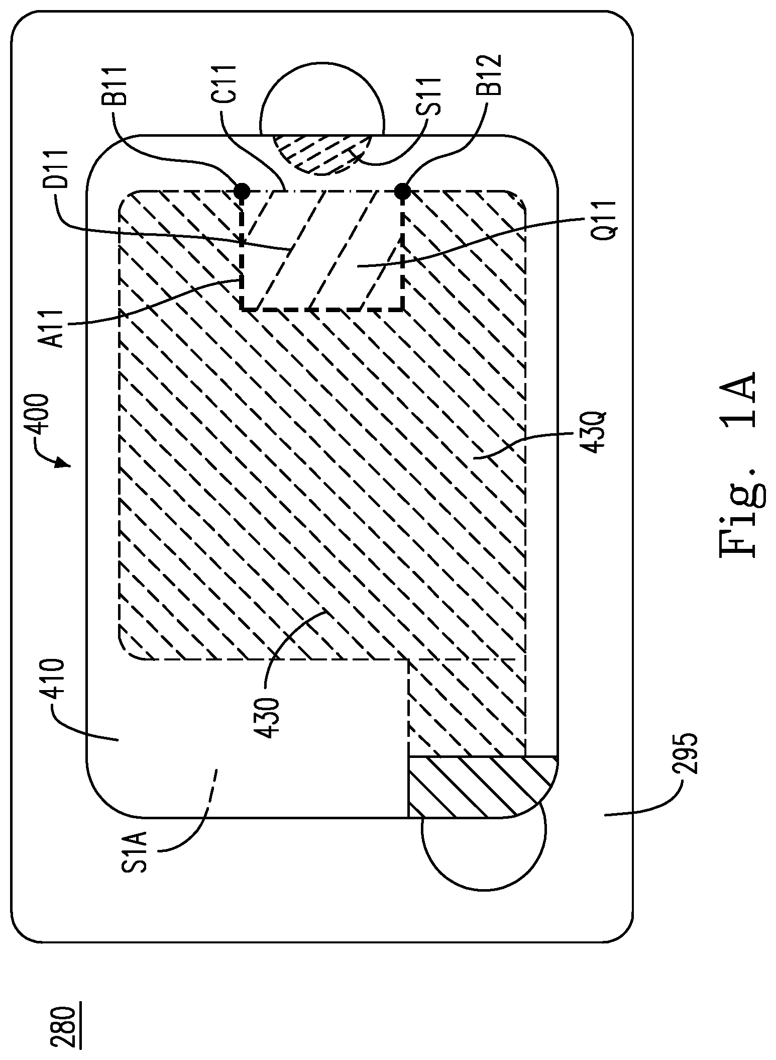
Please refer to A , B and C . A is a schematic diagram showing a top view of a crystal device 280 according to various embodiments of the present disclosure. B is a schematic diagram showing a front view of the crystal device 280 shown in A . C is a schematic diagram showing a top view of an integrated chip 400 included in the crystal device 280 shown in A . As shown in A, 1 B and 1 C , the crystal device 280 includes a bearing structure 295 and the integrated chip 400 supported by the bearing structure 295 . The integrated chip 400 includes a crystal chip 410 and a first excitation electrode 430 . The crystal chip 410 includes a first main surface S 1 A having a first support surface portion S 11 . For example, the first support surface portion S 11 is in contact with the bearing structure 295 .
The first excitation electrode 430 is disposed on the first main surface S 1 A, has an electrode area 43 Q, and includes a first electrode indentation boundary A 11 , wherein the first support surface portion S 11 is partly encompassed by the first electrode indentation boundary A 11 . For example, the first electrode indentation boundary A 11 has a first boundary end B 11 and a second boundary end B 12 being opposite to the first boundary end B 11 . The first electrode indentation boundary A 11 and a first reference line segment C 11 defined by the first and the second boundary ends B 11 and B 12 form a first electrode indentation region D 11 having an indentation area Q 11 . A ratio of the indentation area Q 11 to the electrode area 43 Q ranges from 0.05 to 0.2.
Please refer to A , B and C . A is a schematic diagram showing a top view of an implementation structure 28 A of the crystal device 280 shown in A . B is a schematic diagram showing a front view of the implementation structure 28 A shown in A . C is a schematic diagram showing a top view of an integrated chip 400 included in the implementation structure 28 A shown in A . Please additionally refer to A, 1 B and 1 C . As shown in A, 2 B and 2 C , the crystal device 280 includes the bearing structure 295 and the integrated chip 400 .
In some embodiments, the first electrode indentation region D 11 is adjacent to the first support surface portion S 11 , and further has a first indentation regional center E 11 . The first main surface S 1 A further has a second support surface portion S 12 being separate from the first support surface portion S 11 . For example, the second support surface portion S 12 is in contact with the bearing structure 295 . The first excitation electrode 430 further includes a second electrode indentation boundary A 12 , wherein the second support surface portion S 12 is partly encompassed by the second electrode indentation boundary A 12 . For example, the first support surface portion S 11 is partly encompassed by the first electrode indentation boundary A 11 . The second support surface portion S 12 is locally encompassed by the second electrode indentation boundary A 12 .
For example, the second electrode indentation boundary A 12 has a third boundary end B 13 and a fourth boundary end B 14 being opposite to the third boundary end B 13 . The second electrode indentation boundary A 12 and a second reference line segment C 12 defined by the third and the fourth boundary ends B 1 and B 14 form a second electrode indentation region D 12 having a second indentation regional center E 12 . The second electrode indentation region D 12 further has an indentation area Q 12 . A ratio of the indentation area Q 12 to the electrode area 43 Q ranges between 0.05 and 0.2. For example, the indentation area Q 12 is substantially equal to the indentation area Q 11 .
The crystal chip 410 has a centroid HH 1 . The centroid HH 1 and the first indentation regional center E 11 define a third reference line segment L 11 therebetween. The centroid HH 1 and the second indentation regional center E 12 define a fourth reference line segment L 12 therebetween. An included angle N 12 formed between the third and the fourth reference line segments L 11 and L 12 ranges from 30 degrees to 90 degrees. For example, the first and the second reference line segments C 11 and C 12 are respectively two reference straight line segments. Preferably, the included angle N 12 ranges from 50 degrees to 70 degrees.
In some embodiments, the crystal chip 410 has a centroid HH 1 . The first electrode indentation region D 11 has a first indentation regional center E 11 . The integrated chip 400 further includes a first extension electrode 440 . The first extension electrode 440 extends from the first excitation electrode 430 , and includes a first signal transmission terminal 445 being in contact with the bearing structure 295 . The first signal transmission terminal 445 has a first support regional center UJ 1 . The centroid HH 1 and the first support regional center UJ 1 define a second reference line segment LU 1 therebetween. The centroid HH 1 and the first indentation regional center E 11 define a third reference line segment L 11 therebetween. A first included angle N 11 formed between the second and the third reference line segments LU 1 and L 11 ranges from 100 degrees to 220 degrees. For example, the first signal transmission terminal 445 includes a support region VJ 1 . The support region VJ 1 has the first support regional center UJ 1 . Preferably, the first included angle N 11 ranges from 140 degrees to 180 degrees.
The first support surface portion S 11 has an edge T 11 being opposite to the first electrode indentation boundary A 11 . The first indentation regional center E 11 and the edge T 11 define a shortest distance F 11 therebetween. The centroid HH 1 and the edge T 11 define a shortest distance G 11 therebetween. A ratio of the shortest distance F 11 to the shortest distance G 11 ranges from 0.03 to 0.2. The second support surface portion S 12 has an edge T 12 being opposite to the second electrode indentation boundary A 12 . The second indentation regional center E 12 and the edge T 12 define a shortest distance F 12 therebetween. The centroid HH 1 and the edge T 12 define a shortest distance G 12 therebetween. A ratio of the shortest distance F 12 to the shortest distance G 12 ranges from 0.03 to 0.2. For example, the first electrode indentation boundary A 11 includes a first straight line segment 11 A and a second straight line segment 11 B being adjacent to the first straight line segment 11 A.
Please refer to A , B and C . A is a schematic diagram showing a top view of an implementation structure 28 B of the crystal device 280 shown in A . B is a schematic diagram showing a rear view of the implementation structure 28 B shown in A . C is a schematic diagram showing a top view of an integrated chip 400 included in the implementation structure 28 B shown in A . Please additionally refer to A, 1 B, 1 C, 2 A, 2 B and 2 C . As shown in A, 3 B and 3 C , the crystal device 280 includes the bearing structure 295 and the integrated chip 400 .
In some embodiments, the crystal device 280 is or includes a quartz crystal resonator. The crystal chip 410 is or includes a quartz chip, and further includes a second main surface S 2 A being opposite to the first main surface S 1 A. The integrated chip 400 further includes a second excitation electrode 450 and a second extension electrode 460 extending from the second excitation electrode 450 . The second excitation electrode 450 is disposed on the second main surface S 2 A, and includes a second electrode indentation boundary A 21 matching the first electrode indentation boundary A 11 . The second extension electrode 460 includes a second signal transmission terminal 465 being in contact with the bearing structure 295 . The second signal transmission terminal 465 has a second support regional center UJ 2 . The centroid HH 1 and the second support regional center UJ 2 define a fourth reference line segment LU 2 therebetween. A second included angle NU 1 formed between the second and the fourth reference line segments LU 1 and LU 2 ranges from 30 degrees to 90 degrees. For example, preferably, the second included angle NU 1 ranges from 50 degrees to 70 degrees.
The bearing structure 295 includes a bearing base 300 , a bonding adhesive W 1 A, a first conductive adhesive W 7 A and a second conductive adhesive W 8 A. The bearing base 300 includes a first conductive seat 320 , a second conductive seat 340 being separate from the first conductive seat 320 , and a support platform 360 . The bonding adhesive W 1 A is at least partly disposed between the support platform 360 and the first support surface portion S 11 . The first conductive adhesive W 7 A is at least partly disposed between the first conductive seat 320 and the first signal transmission terminal 445 . The second conductive adhesive W 8 A is at least partly disposed between the second conductive seat 340 and the second signal transmission terminal 465 .
In some embodiments, the bearing structure 295 further includes a bonding adhesive W 2 A. The bearing base 300 further includes a support platform 362 . The bonding adhesive W 2 A is at least partly disposed between the support platform 362 and the second support surface portion S 12 . The second excitation electrode 450 further includes an electrode indentation boundary A 22 matching the second electrode indentation boundary A 12 . For example, the second signal transmission terminal 465 includes a support region VJ 2 . The support region VJ 2 has the second support regional center UJ 2 . For example, the second electrode indentation boundary A 21 includes a first straight line segment 21 A and a second straight line segment 21 B being adjacent to the first straight line segment 21 A.
The second excitation electrode 450 matches the first excitation electrode 430 , and has an electrode area 45 Q. The electrode area 45 Q is substantially equal to the electrode area 43 Q. The second electrode indentation boundary A 21 corresponds to the first electrode indentation boundary A 11 , and has a boundary end B 21 and a boundary end B 22 being opposite to the boundary end B 21 . The second electrode indentation boundary A 21 and a reference line segment C 21 defined by the boundary ends B 21 and B 22 form an electrode indentation region D 21 having an indentation area Q 21 . The indentation area Q 21 is substantially equal to the indentation area Q 11 . A ratio of the indentation area Q 21 to the electrode area 45 Q ranges from 0.05 to 0.2. The electrode indentation region D 21 further has an indentation regional center E 21 .
In some embodiments, the electrode indentation boundary A 22 corresponds to the second electrode indentation boundary A 12 , and has a boundary end B 23 and a boundary end B 24 being opposite to the boundary end B 23 . The electrode indentation boundary A 22 and a reference line segment C 22 defined by the boundary ends B 23 and B 24 form an electrode indentation region D 22 having an indentation regional center E 22 . The electrode indentation region D 22 further has an indentation area Q 22 . A ratio of the indentation area Q 22 to the electrode area 45 Q ranges from 0.05 to 0.2. For example, the indentation area Q 22 is substantially equal to the indentation area Q 12 , and is substantially equal to the indentation area Q 21 .
The centroid HH 1 and the indentation regional center E 21 define a reference line segment L 21 therebetween. The centroid HH 1 and the indentation regional center E 22 define a reference line segment L 22 therebetween. An included angle N 22 formed between the reference line segments L 21 and L 22 ranges from 30 degrees to 90 degrees. For example, the reference line segments C 21 and C 22 are respectively two reference straight line segments. The included angle N 22 is substantially equal to the included angle N 12 . An included angle N 21 formed between the second reference line segment LU 1 and the reference line segment L 21 ranges from 100 degrees to 220 degrees. For example, preferably, the included angle N 22 ranges from 50 degrees to 70 degrees. Preferably, the included angle N 21 ranges from 140 degrees to 180 degrees.
The first main surface S 1 A has four surface corner portions MF 1 , MF 2 , MF 3 and MF 4 . The four surface corner portions MF 1 , MF 2 , MF 3 and MF 4 are located at four different spatial positions, respectively. The four surface corner portions MF 1 , MF 2 , MF 3 and MF 4 have the support region VJ 1 , the support region VJ 2 , the first support surface portion S 11 and the second support surface portion S 12 , respectively.
Please refer to , which is a schematic diagram showing a top view of a crystal system 270 according to various embodiments of the present disclosure. As shown in , the crystal system 270 includes a bearing structure 295 and a resonance element 390 supported by the bearing structure 295 . The resonance element 390 includes a crystal chip 410 and a first excitation electrode 430 . The crystal chip 410 includes a first main surface S 1 A having a first support surface portion S 11 . For example, the first support surface portion S 11 is in contact with the bearing structure 295 .
The first excitation electrode 430 is disposed on the first main surface S 1 A, has an electrode area 43 Q, and includes a first electrode indentation boundary A 11 partly encompassing the first support surface portion S 11 . For example, the first electrode indentation boundary A 11 has a first boundary end B 11 and a second boundary end B 12 being opposite to the first boundary end B 11 . The first electrode indentation boundary A 11 and a first reference line segment C 11 defined by the first boundary end B 11 and the second boundary end B 12 form a first electrode indentation region D 11 having an indentation area Q 11 . A ratio of the indentation area Q 11 to the electrode area 43 Q ranges between 0.05 and 0.2. For example, the resonance element 390 is the integrated chip 400 . The crystal system 270 is the crystal device 280 .
Please refer to , which is a schematic diagram showing a top view of a crystal system 260 according to various embodiments of the present disclosure. As shown in , the crystal system 260 includes a bearing structure 295 and an element 380 supported by the bearing structure 295 . The element 380 includes a crystal chip 410 and an electrode structure 4 A 0 .
The crystal chip 410 has a surface structure SAA. The electrode structure 4 A 0 is disposed on the surface structure SAA, and includes an excitation electrode 430 , an extension electrode 440 having a first signal transmission terminal 445 , and a second signal transmission terminal 465 matching the first signal transmission terminal 445 . For example, the first and the second signal transmission terminals 445 and 465 are disposed on one side 415 of the crystal chip 410 . The extension electrode 440 extends from the excitation electrode 430 . The bearing structure 295 supports the crystal chip 410 through the first and the second signal transmission terminals 445 and 465 . The excitation electrode 430 has a closed boundary KA 1 . The closed boundary KA 1 includes a concave boundary segment K 11 .
Please refer to A , B , C and D . A is a schematic diagram showing a top view of an implementation structure 26 A of the crystal device 260 shown in . B is a schematic diagram showing a front view of the implementation structure 26 A shown in A . C is a schematic diagram showing a top view of the implementation structure 26 A shown in A . D is a schematic diagram showing a front view of the implementation structure 26 A shown in A . Please additionally refer to . As shown in A, 6 B, 6 C and 6 D , the crystal system 260 includes the bearing structure 295 and the element 380 . For example, the element 380 is one of the resonance element 390 and the integrated chip 400 . The crystal system 260 is the crystal device 280 .
In some embodiments, the concave boundary segment K 11 includes a first straight line segment 11 A and a second straight line segment 11 B being adjacent to the first straight line segment 11 A. For example, the second straight line segment 11 B is substantially perpendicular to the first straight line segment 11 A. The surface structure SAA includes a first main surface S 1 A and a second main surface S 2 A being opposite to the first main surface S 1 A. For example, the excitation electrode 430 is disposed on the first main surface S 1 A. Each of the first and the second signal transmission terminals 445 and 465 is at least partly disposed on the first main surface S 1 A. The first main surface S 1 A has a support surface portion S 11 . For example, the support surface portion S 11 is in contact with the bearing structure 295 . The concave boundary segment K 11 is the first electrode indentation boundary A 11 .
The excitation electrode 430 has an electrode area 43 Q. The concave boundary segment K 11 partly encompasses the support surface portion S 11 , and has a first boundary end B 11 and a second boundary end B 12 being opposite to the first boundary end B 11 . The concave boundary segment K 11 and a reference line segment C 11 defined by the first and the second boundary ends B 11 and B 12 form an electrode indentation region D 11 having an indentation area Q 11 . A ratio of the indentation area Q 11 to the electrode area 43 Q ranges from 0.05 to 0.2.
For example, the electrode structure 4 A 0 includes the excitation electrode 430 , the extension electrode 440 , a second excitation electrode 450 and a second extension electrode 460 extending from the second excitation electrode 450 . The second excitation electrode 450 is disposed on the second main surface S 2 A. The second extension electrode 460 has the second signal transmission terminal 465 . The excitation electrode 430 has a geometrical shape 43 M. The geometrical shape 43 M is formed by the closed boundary KA 1 . The closed boundary KA 1 is an outer closed boundary. For example, the concave boundary segment K 11 includes a curve segment.
In some embodiments, the crystal chip 410 further has a major axis YA 1 , a relatively long edge JA 1 and a relatively short edge JB 1 . For example, the major axis YA 1 passes through the centroid HH 1 , and is substantially parallel with the relatively long edge JA 1 . The relatively long edge JA 1 is substantially perpendicular to the relatively short edge JB 1 . The extension electrode 440 extends from the excitation electrode 430 to the relatively short edge JB 1 . The second extension electrode 460 extends from the second excitation electrode 450 to the relatively short edge JB 1 . The first and the second main surfaces S 1 A and S 2 A have a first central portion and a second central portion, respectively. The excitation electrode 430 and the second excitation electrode 450 are respectively disposed on the first and the second central portions.
The geometrical shape 43 M forms at least one indentation to avoid influencing the best excitation mode. The second excitation electrode 450 matches the excitation electrode 430 . The geometrical shape 43 M of the excitation electrode 430 is presented with one of a convex shape and a concave shape, and is different from one of a rectangular shape and a circular shape shown in the prior art. The geometrical shape 43 M includes an irregular shape being one of a convex shape and a concave shape. The excitation electrode 430 may be formed by combining irregular shape electrodes which have shapes selected from a group consisting of a rectangular shape, a circular shape, a concave shape and a convex shape. The excitation electrode 430 has an electrode material; and the electrode material is a conductive material. Any of the first electrode indentation boundary A 11 , the second electrode indentation boundary A 12 and the second electrode indentation boundary A 21 is used for a damping compensation of the resonance element 390 .
An excitation electrode disclosed in the prior art has a specific shape. For example, the specific shape is one selected from a group consisting of a square shape, a rectangular shape and a circular shape. The geometrical shape 43 M of the excitation electrode 430 shown in the present disclosure is different from the specific shape. The excitation electrode 430 having the geometrical shape 43 M causes the resonance element 390 to form a different oscillation strength. The excitation electrode 430 can be used to manufacture the crystal device 280 being or including a quartz-crystal resonator, so that the crystal device 280 can be used for a vehicle. The resonance element 390 including the excitation electrode 430 can be applied to a different adhesive-dispensing mode to increase a design space of the crystal device 280 , can meet a characteristic requirement having the high strength anti-drop, and keeps the original product property under a condition of meeting the characteristic requirement.
For example, the crystal device 280 further includes a lid 500 . The bonding adhesive W 1 A is a conductive adhesive. Each of the bonding adhesive W 1 A, the first conductive adhesive W 7 A and the second conductive adhesive W 8 A is a silver adhesive; and the bonding adhesive W 1 A, the first conductive adhesive W 7 A and the second conductive adhesive W 8 A have the same material. Each of the first excitation electrode 430 , the first extension electrode 440 , the second excitation electrode 450 and the second extension electrode 460 is a metal electrode. For example, the metal electrode is a silver electrode. The first excitation electrode 430 , the first extension electrode 440 , the second excitation electrode 450 and the second extension electrode 460 are associated with frequency adjustment, frequency stability, and electrical property of the product. For example, the lid 500 is an upper lid.
The bearing base 300 has a containment space VC 1 , and includes an insulation seat body 310 , the first conductive seat 320 , and the second conductive seat 340 being separate from the first conductive seat 320 . Each of the first and the second conductive seats 320 and 340 is disposed in the insulation seat body 310 . The insulation seat body 310 includes the support platform 360 , is a ceramic seat body, and is used to fix the first and the second conductive seats 320 and 340 to cause the bearing base 300 to have a signal contact point for the electrical signal. The lid 500 is disposed on the bearing base 300 , and is used to insulate the containment space VC 1 from the external environment and to seal the bearing base 300 . The resonance element 390 is used to form an electrical signal. The first and the second conductive adhesives W 7 A and W 8 A are used to transmit the electrical signal.
The first and the second conductive adhesives W 7 A and W 8 A are respectively disposed on the first and the second conductive seats 320 and 340 . The crystal chip 410 is or includes a quartz chip, and is used to form a frequency signal source. Each of the first and the second conductive adhesives W 7 A and W 8 A is disposed between the integrated chip 400 and the bearing base 300 , serves as a signal transmission medium, and serves as a fixing support point. The first and the second excitation electrodes 430 and 450 are used to excite the crystal chip 410 to oscillate to generate the electrical signal having a frequency. The first extension electrode 440 is used to electrically connect the first excitation electrode 430 and the first conductive adhesive W 7 A. The second extension electrode 460 is used to electrically connect the second excitation electrode 450 and the second conductive adhesive W 8 A.
Please refer to A , B and C . A is a schematic diagram showing a first support of a resonance element 390 according to various embodiments of the present disclosure. B is a schematic diagram showing a second support of a resonance element 390 according to various embodiments of the present disclosure. C is a schematic diagram showing a third support of a resonance element 390 according to various embodiments of the present disclosure. The resonance element 390 has a first side 391 and a second side 392 being opposite to the first side 391 . As shown in A , the first side 391 of the resonance element 390 is fixed to the bearing structure 295 . The resonance element 390 shown in A has a relatively high resonance frequency, is in a first static state at a first time, and is in a first vibration state at a second time being different from the first time. For example, the relatively high resonance frequency is a normal frequency that is generally used.
As shown in B , the first side 391 of the resonance element 390 is fixed to the bearing structure 295 . The resonance element 390 shown in B has a relatively low resonance frequency, is in a second static state at a third time, and is in a second vibration state at a fourth time being different from the third time. As shown in C , each of the first and the second sides 391 and 392 of the resonance element 390 is fixed to the bearing structure 295 . The resonance element 390 shown in C has a relatively low resonance frequency, is in a third static state at a fifth time, and is in a third vibration state at a sixth time being different from the fifth time. For example, the relatively low resonance frequency is equal to 8 M Hz.
The thickness of the crystal chip 410 is increased with the reduction of the resonance frequency. Under a condition that the thickness of the crystal chip 410 is increased, the angle of the resonance element 390 being available to be offset is reduced when the resonance element 390 is disposed onto the bearing structure 295 . Under a condition that the thickness of the crystal chip 410 is increased, the weight of the crystal chip 410 rises so as to easily cause the resonance element 390 to deform downward, thereby causing the crystal chip 410 to touch the insulation seat body 310 . Under a condition that the crystal chip 410 touches the insulation seat body 310 , the oscillation of the crystal chip 410 can cause the electricity to be unstable, so that the use of a specific adhesive-dispensing method can limit the space which the chip deforms downward. However, the specific adhesive-dispensing method can also cause the electrical property to change, so that the use of a specific electrode may adjust the changed electrical property caused due to the change of the adhesive-dispensing method.
In some embodiments, because the thickness of the crystal chip 410 is increased, the bonding adhesive W 1 A is at least partly disposed between the support platform 360 and the first support surface portion S 11 of the crystal chip 410 to prevent the crystal chip 410 from downward deformation, thereby increasing the oscillation stability of the crystal chip 410 . Under a condition that the bonding adhesive W 1 A is at least partly disposed between the support platform 360 and the first support surface portion S 11 and the first excitation electrode 430 is too close to the first support surface portion S 11 , the oscillation formed by the resonance element 390 can have a phenomenon of frequency instability. For example, the first support surface portion S 11 is included in the second side 392 of the resonance element 390 .
In order to solve the phenomenon of frequency instability, the geometrical shape of the original excitation electrode is changed to the geometrical shape 43 M, so that the original excitation electrode is changed to the first excitation electrode 430 . Therefore, the first excitation electrode 430 includes the first electrode indentation boundary A 11 , partly encompassing the first support surface portion S 11 , to increase the oscillation stability of the crystal chip 410 . The first excitation electrode 430 has he electrode area 43 Q. The first electrode indentation boundary A 11 and the first reference line segment C 11 form the first electrode indentation region D 11 having the indentation area Q 11 . A ratio of the indentation area Q 11 to the electrode area 43 Q ranges from 0.05 to 0.2. Therefore, the original oscillation property of the resonance element 390 can be kept. The geometrical shape and the size of the first excitation electrode 430 can affect the oscillation property of the resonance element 390 .
Please refer to A , B , C and D . A is a first schematic structure diagram showing a first resonance element 395 according to various embodiments of the present disclosure. B is a second schematic structure diagram showing a second resonance element 396 according to various embodiments of the present disclosure. C is a third schematic structure diagram showing a third resonance element 397 according to various embodiments of the present disclosure. D is a fourth schematic structure diagram showing a fourth resonance element 398 according to various embodiments of the present disclosure. The first, the second, the third and the fourth resonance elements 395 , 396 , 397 and 398 respectively include an excitation electrode 455 , an excitation electrode 456 , an excitation electrode 457 and an excitation electrode 458 .
The excitation electrode 455 has a relatively large electrode area. The excitation electrode 456 has two corner indentations R 11 and R 12 , and a first specific electrode area. The excitation electrode 457 has a relatively small electrode area. The excitation electrode 457 has a side indentation R 21 and a second specific electrode area. Each of the first and the second specific electrode areas is greater than the relatively small electrode area, and is less than the relatively large electrode area.
Simulations performed to the first, the second, the third and the fourth resonance elements 395 , 396 , 397 and 398 can obtain a plurality of simulation results. The first, the second, the third and the fourth resonance elements 395 , 396 , 397 and 398 respectively have different geometrical shapes, and thereby respectively form a first oscillation range, a second oscillation range, a third oscillation range and a fourth oscillation range. The first, the second, the third and the fourth oscillation ranges are different. The larger an excitation electrode is, the wider the formed oscillation range is. That is, under a condition that the first, the second, the third and the fourth resonance elements 395 , 396 , 397 and 398 are not supported, each of the second and the third oscillation ranges is less than the first oscillation range, and the third oscillation range is less than the fourth oscillation range.
Although the first specific electrode area of the excitation electrode 456 is less than the relatively large electrode area of the excitation electrode 455 , the second oscillation range of the second resonance element 396 can be approximate to the first oscillation range of the first resonance element 395 by using the two corner indentations R 11 and R 12 . Although the second specific electrode area of the excitation electrode 458 is less than the relatively large electrode area of the excitation electrode 455 , the fourth oscillation range of the fourth resonance element 398 can be approximate to the first oscillation range of the first resonance element 395 by using the side indentation R 21 .
Please refer to A, 2 A, 3 A, 8 A, 8 B, 8 C and 8 D . Under a condition that the first excitation electrode 430 is even more close to the bonding adhesive W 1 A, the oscillation range of the resonance element 390 can be influenced to shrink inwards. Under a condition that the first excitation electrode 430 is even more away from the bonding adhesive W 1 A, the oscillation range of the resonance element 390 is even more less influenced. For example, the damping ratio for the first electrode indentation region D 11 of the resonance element 390 ranges from 5% to 15%.
Please refer to A and B . A is a schematic diagram showing a measured frequency changed with a temperature for the second resonance element 396 shown in B . B is a schematic diagram showing a measured impedance changed with a temperature for the second resonance element 396 shown in B . As shown in A and 9 B , the excitation electrode 456 can cause the resistance of the second resonance element 396 to change at different temperatures, and can cause the resistance of the second resonance element 396 to increase at a relatively low temperature.
While the invention has been described in terms of what is presently considered to be the most practical and preferred embodiments, it is to be understood that the disclosure need not be limited to the disclosed embodiments. On the contrary, it is intended to cover various modifications and similar arrangements included within the spirit and scope of the appended claims, which are to be accorded with the broadest interpretation so as to encompass all such modifications and similar structures.
Figures (20)
Citations
This patent cites (3)
- US7915791
- US20090085428
- US20150108875