Abstract
In this power conversion device, first three-phase AC voltages generated by an inverter and an AC filter are divided by first to third voltage dividers to generate second three-phase AC voltages, and third three-phase AC voltages that are line-to-line voltages of the second three-phase AC voltages and a neutral point voltage of the first three-phase AC voltages are detected. Then, DC components of the third three-phase AC voltages resulting from errors of voltage ratios of the first to third voltage dividers are obtained based on the detection results and contents in a storage unit, the DC components are removed from the third three-phase AC voltages to generate fourth three-phase AC voltages, and the inverter is controlled such that DC components of the fourth three-phase AC voltages are eliminated.
Claims (8)
1. A power conversion device comprising: a reverse converter that converts DC voltage into first three-phase AC voltages; first to third voltage dividers that divide the first three-phase AC voltages to generate second three-phase AC voltages; first to third voltage detectors that detect third three-phase AC voltages that are line-to-line voltages of the second three-phase AC voltages; a fourth voltage detector that detects a neutral point voltage of the first three-phase AC voltages; a storage unit in which information related to errors of voltage division ratios of the first to third voltage dividers is stored; a correction unit that obtains first DC components resulting from the errors of voltage division ratios in the third three-phase AC voltages, based on detection results of the first to fourth voltage detectors and contents in the storage unit, and removes the obtained first DC components from the third three-phase AC voltages to generate fourth three-phase AC voltages; and a control unit that controls the reverse converter such that second DC components of the fourth three-phase AC voltages are eliminated.
Show 7 dependent claims
2. The power conversion device according to claim 1 , wherein the information stored in the storage unit includes a first error of voltage division ratios of the first and second voltage dividers, a second error of voltage division ratios of the second and third voltage dividers, and a third error of voltage division ratios of the third and first voltage dividers, and the correction unit obtains the first DC components resulting from the errors of voltage division ratios in the third three-phase AC voltages by multiplying the neutral point voltage detected by the fourth voltage detector by the first to third errors stored in the storage unit.
3. The power conversion device according to claim 2 , further comprising a DC detector that detects fourth DC components of the third three-phase AC voltages, wherein the first to third errors are obtained by operating the reverse converter in a state in which a load is not connected to the reverse converter and dividing the fourth DC components of the third three-phase AC voltages detected by the DC detector by the neutral point voltage detected by the fourth voltage detector.
4. The power conversion device according to claim 1 , wherein the first three-phase AC voltages are supplied to a load, the power conversion device further comprises: first to third current detectors that detect three-phase AC currents flowing from the reverse converter to the load; and a first DC detector that detects fifth DC components of the three-phase AC currents detected by the first to third current detectors, the information stored in the storage unit includes first to third coefficients, and the correction unit obtains the first DC components resulting from the errors of voltage division ratios in the third three-phase AC voltages by multiplying the neutral point voltage detected by the fourth voltage detector by the first to third coefficients and further multiplying by the fifth DC components of the three-phase AC currents detected by the first DC detector.
5. The power conversion device according to claim 4 , further comprising a second DC detector that detects fourth DC components of the third three-phase AC voltages, wherein the first to third coefficients are obtained by (i) controlling the reverse converter such that the DC components of the third three-phase AC voltages detected by the first to third voltage detectors are eliminated in a state in which a load is connected to the reverse converter, (ii) thereafter controlling the reverse converter such that the fifth DC components of the three-phase AC currents detected by the first DC detector are reduced, (iii) dividing the fourth DC components of the third three-phase AC voltages detected by the second DC detector by the fifth DC components of the three-phase AC currents detected by the first DC detector, and (iv) further dividing by the neutral point voltage detected by the fourth voltage detector.
6. The power conversion device according to claim 1 , wherein the reverse converter includes an inverter that converts the DC voltage into three-phase pulse signal trains, and an AC filter that converts the three-phase pulse signal trains into the first three-phase AC voltages and outputs the first three-phase AC voltages to first to third output terminals, the AC filter includes first to third reactors and first to third capacitors, the first to third reactors have first terminals respectively receiving the three-phase pulse signal trains and have second terminals respectively connected to the first to third output terminals, and the first to third capacitors have first electrodes respectively connected to the first to third output terminals and have second electrodes commonly receiving the neutral point voltage.
7. The power conversion device according to claim 1 , wherein the first voltage divider includes first and second resistor elements, the second voltage divider includes third and fourth resistor elements, the third voltage divider includes fifth and sixth resistor elements, the first, third, and fifth resistor elements have first terminals respectively connected to first to third output terminals of the reverse converter and have second terminals respectively connected to first to third monitor terminals, the second, fourth, and sixth resistor elements have first terminals respectively connected to the first to third monitor terminals and have second terminals commonly receiving a reference voltage, the first voltage detector detects a voltage between the first and second monitor terminals, the second voltage detector detects a voltage between the second and third monitor terminals, and the third voltage detector detects a voltage between the third and first monitor terminals.
8. The power conversion device according to claim 1 , wherein the first three-phase AC voltages are supplied to a load, the load includes a load body and a three-phase transformer that transmits the first three-phase AC voltages to the load body.
Full Description
Show full text →
TECHNICAL FIELD
The present invention relates to a power conversion device and more particularly to a power conversion device including a reverse converter that converts DC voltage into three-phase AC voltage.
BACKGROUND ART
For example, Patent Literature 1 discloses a power conversion device including a reverse converter that converts DC voltage into AC voltage, a transformer that transmits AC output voltage from the reverse converter to a load, and a control device that controls the reverse converter such that a DC component of the AC output voltage is eliminated, thereby preventing occurrence of an asymmetrical excitation phenomenon in the transformer.
CITATION LIST
Patent Literature
• PTL 1: Japanese Patent Laying-Open No. 2018-207785
SUMMARY OF INVENTION
Technical Problem
In general, in such a power conversion device, a first AC voltage output from the reverse converter is divided to generate a second AC voltage, and the reverse converter is controlled such that a DC component of the second AC voltage is eliminated. When first three-phase AC voltages are generated by the reverse converter, the first three-phase AC voltages are divided by first to third voltage dividers to generate second three-phase AC voltages, and the reverse converter is controlled such that DC components of third three-phase AC voltages that are the line-to-line voltages of the second three-phase AC voltages are eliminated.
However, when the voltage division ratios of the first to third voltage dividers are not identical, DC components resulting from errors of voltage ratios of the first to third voltage dividers are included in the third three-phase AC voltages, so that the reverse converter is unable to be controlled accurately.
A main object of the present invention is therefore to provide a power conversion device capable of accurately controlling the reverse converter even when the voltage ratios of the first to third voltage dividers are not identical.
Solution to Problem
A power conversion device according to the present invention includes a reverse converter, first to third voltage dividers, first to third voltage detectors, a fourth voltage detector, a storage unit, a correction unit, and a control unit. The reverse converter converts DC voltage into first three-phase AC voltages. The first to third voltage dividers divide the first three-phase AC voltages to generate second three-phase AC voltages. The first to third voltage detectors detect third three-phase AC voltages that are line-to-line voltages of the second three-phase AC voltages. The fourth voltage detector detects a neutral point voltage of the first three-phase AC voltages. The storage unit stores information related to errors of voltage division ratios of the first to third voltage dividers. The correction unit obtains DC components resulting from the errors of voltage division ratios in the third three-phase AC voltages, based on detection results of the first to fourth voltage detectors and contents in the storage unit. The correction unit removes the obtained DC components from the third three-phase AC voltages to generate fourth three-phase AC voltages. The control unit controls the reverse converter such that DC components of the fourth three-phase AC voltages are eliminated.
Advantageous Effects of Invention
In this power conversion device, the first three-phase AC voltages output from the reverse converter are divided by the first to third voltage dividers to generate the second three-phase AC voltages, and the third three-phase AC voltages that are line-to-line voltages of the second three-phase AC voltages and the neutral point voltage of the first three-phase AC voltages are detected. Then, DC components resulting from errors of voltage ratios in the third three-phase AC voltages are obtained based on the detection results and contents in the storage unit, the DC components are removed from the third three-phase AC voltages to generate the fourth three-phase AC voltages, and the reverse converter is controlled such that DC components of the fourth three-phase AC voltages are eliminated. The reverse converter therefore can be controlled accurately even when the voltage division ratios of the first to third voltage dividers are not identical.
BRIEF DESCRIPTION OF DRAWINGS
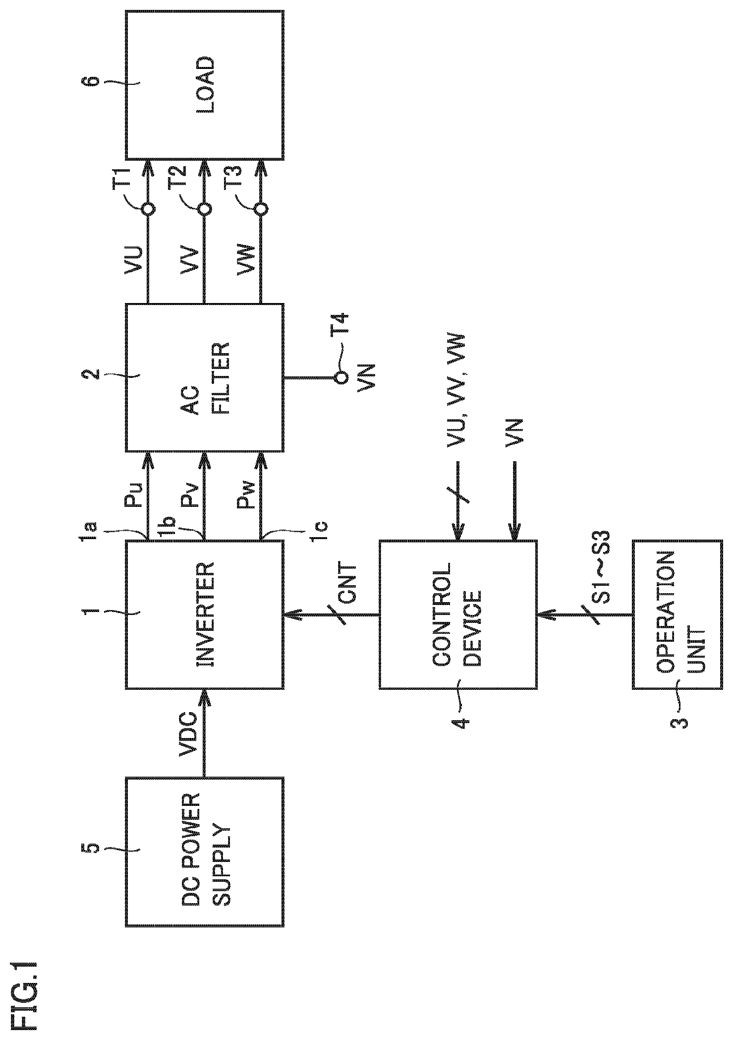
is a block diagram showing a configuration of a power conversion device according to a first embodiment.
is a circuit diagram showing a configuration of an AC filter shown in .
is a circuit block diagram illustrating a configuration of a load shown in .
is a block diagram showing a configuration of a control device shown in .
is a circuit block diagram showing a configuration of three-phase voltage dividers and line-to-line voltage detectors shown in .
is a block diagram showing a configuration of a control unit shown in .
is a block diagram showing the main part of a modification to the first embodiment.
is a block diagram showing a configuration of a power conversion device according to a second embodiment.
is a block diagram showing a configuration of a control device shown in .
is a block diagram showing a configuration of a control unit shown in .
DESCRIPTION OF EMBODIMENTS
First Embodiment
is a block diagram showing a configuration of a power conversion device according to a first embodiment. In , this power conversion device includes an inverter 1 , an AC filter 2 , an operation unit 3 , a control device 4 , and output terminals T 1 to T 3 .
Inverter 1 is controlled by a control signal CNT supplied from control device 4 . Inverter 1 includes, for example, six IGBTs (Insulated Gate Bipolar Transistors) and six diodes respectively connected in anti-parallel with the six IGBTs. Control signal CNT includes six gate signals for respectively turning on and off the six IGBTs. Each of the six gate signals is a PWM (Pulse Width Modulation) signal.
Inverter 1 converts a DC voltage VDC supplied from a DC power supply 5 into three-phase pulse signal trains Pu, Pv, and Pw having a commercial frequency, which are output to output nodes 1 a , 1 b , and 1 c . DC power supply 5 may be a battery or may be a forward converter that converts AC voltage supplied from a commercial AC power supply into DC voltage.
is a circuit diagram showing a configuration of AC filter 2 . In , AC filter 2 includes reactors L 1 to L 3 and capacitors C 1 to C 3 . Reactors L 1 to L 3 have first terminals respectively connected to output nodes 1 a to 1 c of inverter 1 and second terminals respectively connected to output terminals T 1 to T 3 . Capacitors C 1 to C 3 have first electrodes respectively connected to output terminals T 1 to T 3 and second electrodes connected commonly to a neutral point terminal T 4 .
A neutral point voltage VN is produced between neutral point terminal T 4 and a line of ground voltage GND (reference voltage). Neutral point voltage VN is DC voltage and fluctuates with the environment in which the power conversion device is installed. Neutral point voltage VN is detected by control device 4 .
AC filter 2 is a low pass filter, passes AC components having a commercial frequency of three-phase pulse signal trains Pu, Pv, and Pw output from inverter 1 , and cuts off a signal having a switching frequency. In other words, AC filter 2 converts three-phase pulse signal trains Pu, Pv, and Pw into three-phase AC voltages VU, VV, and VW (first three-phase AC voltages) having a commercial frequency.
Three-phase AC voltages VU, VV, and VW include AC voltages Vu, Vv, and Vw, respectively, and neutral point voltage VN. That is, VU=Vu+VN, VV=Vv+VN, and VW=Vw+VN. Each of AC voltages Vu, Vv, and Vw changes sinusoidally with a commercial frequency. AC voltages Vu, Vv, and Vw are out of phase by 120 degrees. Instantaneous values of three-phase AC voltages VU, VV, and VW are detected by control device 4 .
Returning to , load 6 is connected to output terminals T 1 to T 3 . Load 6 is driven by three-phase AC voltages VU, VV, and VW supplied from the power conversion device. is a circuit block diagram illustrating a configuration of load 6 . In , load 6 includes a three-phase transformer 7 and a load body 8 .
Three-phase transformer 7 may be of any of delta-delta type, delta-star type, star-delta type, and star-star type. shows three-phase transformer 7 of delta-delta type.
Three-phase transformer 7 includes primary terminals T 11 to T 13 , secondary terminals T 14 to T 16 , primary windings 7 a to 7 c , and secondary windings 7 d to 7 f . Primary terminals T 11 to T 13 respectively receive three-phase AC voltage VU, VV, and VW passing through AC filter 2 . Secondary terminals T 14 to T 16 are connected to load body 8 .
Primary windings 7 a to 7 c have first terminals respectively connected to primary terminals T 11 , T 12 , and T 143 and have second terminals respectively connected to primary terminals T 12 , T 13 , and T 11 . Secondary windings 7 d to 7 f have first terminals respectively connected to secondary terminals T 14 , T 15 , and T 16 and have second terminals respectively connected to secondary terminals T 15 , T 16 , and T 14 .
Three-phase AC voltages Va, Vb, and Vc having a level corresponding to AC components Vu, Vv, and Vw of three-phase AC voltages VU, VV, and VW are output to secondary terminals T 14 to T 16 . Load body 8 is driven by three-phase AC voltages Va to Vc supplied from three-phase transformer 7 .
When three-phase AC voltages VU, VV, and VW are applied to primary windings 7 a to 7 c of three-phase transformer 7 and current flows through windings 7 a to 7 f , a magnetic flux is generated in the core (not shown). Generation of a DC component in the magnetic flux in the core is referred to as asymmetrical excitation. When asymmetrical excitation occurs, exciting current of three-phase transformer 7 increases, and the waveforms of three-phase AC voltages VU, VV, and VW may be deteriorated, or overcurrent may flow through three-phase transformer 7 to cause breakage of the power converter. In such a power conversion device, therefore, it is necessary to prevent occurrence of an asymmetrical excitation phenomenon in three-phase transformer 7 .
Returning to , operation unit 3 includes a plurality of switches and a plurality of buttons operated by the user of the power conversion device, and an image display unit presenting a variety of information. The user of the power conversion device can operate operation unit 3 to power on and off the power conversion device or select one of an error detection mode and an operation mode.
Operation unit 3 outputs an error detection signal S 1 when giving an instruction to perform an error detection mode, outputs an operation command signal S 2 when giving an instruction to operate load 6 , and outputs an operation stop signal S 3 when giving an instruction to stop the operation of load 6 . Control device 4 generates and applies control signal CNT to inverter 1 , based on signals S 1 to S 3 from operation unit 3 , three-phase AC voltages VU, VV, and VW, neutral point voltage VN, and the like. The error detection mode will be described later.
is a block diagram showing a configuration of control device 4 . In , control device 4 includes a three-phase voltage divider 10 , a line-to-line voltage detector 11 , a voltage detector 12 , a LPF (Low Pass Filter) 13 , a calculation control unit 14 , a storage unit 15 , a subtracter 16 , and a control unit 17 .
Three-phase voltage divider 10 divides three-phase AC voltages VU, VV, and VW output to output terminals T 1 to T 3 ( ) to generate three-phase AC voltages V 1 to V 3 (second three-phase AC voltages). Line-to-line voltage detector 11 detects line-to-line voltages V 12 =V 1 −V 2 , V 23 =V 2 −V 3 , and V 31 =V 3 −V 1 of three-phase AC voltages V 1 to V 3 and outputs three-phase AC signals Vuv, Vvw, and Vwu indicating the detected values of line-to-line voltages V 12 , V 23 , and V 31 (third three-phase AC voltages).
is a circuit block diagram showing a configuration of three-phase voltage divider 10 and line-to-line voltage detector 11 . In , three-phase voltage divider 10 includes voltage dividers 21 to 23 . Voltage divider 21 includes resistor elements 21 a and 21 b and a monitor terminal 21 c . Resistor element 21 a has a first terminal receiving AC voltage VU=Vu+VN and a second terminal connected to monitor terminal 21 c . Resistor element 21 b has a first terminal connected to monitor terminal 21 c and a second terminal receiving ground voltage GND (reference voltage). Letting the resistances of resistor elements 21 a and 21 b be R 1 and R 2 , respectively, the voltage division ratio A of voltage divider 21 is A=R 2 /(R 1 +R 2 ). In other words, AC voltage V 1 =(Vu+VN)A is output to monitor terminal 21 c.
Voltage divider 22 includes resistor elements 22 a and 22 b and a monitor terminal 22 c . Resistor element 22 a has a first terminal receiving AC voltage VV=Vv+VN and a second terminal connected to monitor terminal 22 c . Resistor element 22 b has a first terminal connected to monitor terminal 22 c and a second terminal receiving ground voltage GND. Letting the resistances of resistor elements 22 a and 22 b be R 3 and R 4 , respectively, the voltage division ratio B of voltage divider 22 is B=R 4 /(R 3 +R 4 ). AC voltage V 2 =(Vv+VN)B is output to monitor terminal 22 c.
Voltage divider 23 includes resistor elements 23 a and 23 b and a monitor terminal 23 c . Resistor element 23 a has a first terminal receiving AC voltage VW=Vw+VN and a second terminal connected to monitor terminal 23 c . Resistor element 23 b has a first terminal connected to monitor terminal 23 c and a second terminal receiving ground voltage GND. Letting the resistances of resistor elements 23 a and 23 b be R 5 and R 6 , respectively, the voltage division ratio C of voltage divider 23 is C=R 6 /(R 5 +R 6 ). AC voltage V 3 =(Vw+VN)C is output to monitor terminal 23 c.
Line-to-line voltage detector 11 includes voltage detectors 24 to 26 . Voltage detector 24 detects a voltage V 12 =V 1 −V 2 =VuA−VvB+VN(A−B) that is the difference between AC output voltage V 1 =(Vu+VN)A of voltage divider 21 and AC output voltage V 2 =(Vv+VN)B of voltage divider 22 and outputs an AC signal Vuv indicating the detected line-to-line voltage V 12 .
Voltage detector 25 detects a voltage V 23 =V 2 −V 3 =VvB−VwC+VN(B−C) that is the difference between AC output voltage V 2 =(Vv+VN)B of voltage divider 22 and AC output voltage V 3 =(Vw+VN)C of voltage divider 23 and outputs an AC signal Vvw indicating the detected line-to-line voltage V 23 .
Voltage detector 26 detects a voltage V 31 =V 3 −V 1 =VwC−VuA+VN(C−A) that is the difference between output voltage V 3 =(Vw+VN)C of voltage divider 23 and output voltage V 1 =(Vu+VN)A of voltage divider 21 and outputs an AC signal Vwu indicating the detected line-to-line voltage V 31 .
In actuality, the voltages of three-phase AC signals Vuv, Vvw, and Vwu are smaller than line-to-line voltages V 12 , V 23 , and V 31 . However, here, it is assumed that the voltages of three-phase AC signals Vuv, Vvw, and Vwu are identical to line-to-line voltages V 12 , V 23 , and V 31 for the sake of brevity of explanation.
The reason for detecting line-to-line voltages V 12 , V 23 , and V 31 is to facilitate control of inverter 1 by removing neutral point voltage VN. Here, when the voltage division ratios A, B, and C of voltage dividers 21 , 22 , and 23 are identical, all of DC components VN(A−B), VN(B−C), VN(C−A) of line-to-line voltages V 12 , V 23 , and V 31 are zero, and V 12 =(Vu−Vv)A, V 21 =(Vv−Vw)A, V 31 =(Vw−Vu)A, and each of V 12 , V 23 , and V 31 only includes an AC component.
However, in actuality, the voltage division ratios A, B, and C of voltage dividers 21 , 22 , and 23 do not agree because of manufacturing variations of resistor elements 21 a , 21 b , 22 a , 22 b , 23 a , and 23 b , and errors E 1 =A−B, E 2 =B−C, and E 3 =C−A occur in voltage division ratios A, B, and C.
Line-to-line voltages V 12 , V 23 , and V 31 therefore have DC components VN×E 1 , VN×E 2 , and VN×E 3 resulting from errors E 1 , E 2 , and E 3 of voltage division ratios A, B, and C. If inverter 1 is controlled based on such line-to-line voltages V 12 , V 23 , and V 31 (that is, AC signals Vuv, Vvw, and Vwu), inverter 1 fails to be controlled accurately, and occurrence of an asymmetrical excitation phenomenon in the three-phase transformer fails to be prevented.
In the present first embodiment, errors E 1 , E 2 , and E 3 of voltage division ratios A, B, and C are detected and stored, DC components VN×E 1 , VN×E 2 , and VN×E 3 are obtained by multiplying the stored errors E 1 to E 3 by neutral point voltage VN, and line-to-line voltages V 12 , V 23 , and V 31 (that is, AC signals Vuv, Vvw, and Vwu) are corrected based on these DC components VN×E 1 , VN×E 2 , and VN×E 3 .
Returning to , voltage detector 12 detects neutral point voltage VN and outputs a DC signal Vn indicating the detected value. LPF 13 (DC detector) extracts DC components VD 1 to VD 3 from three-phase AC signals Vuv, Vvw, and Vwu output from voltage detectors 24 to 26 and applies the extracted DC components VD 1 to VD 3 to calculation control unit 14 .
In the error detection mode in which errors E 1 , E 2 , and E 3 of voltage division ratios A, B, and C are detected, the user of the power conversion device does not connect load 6 to output terminals T 1 to T 3 ( ) but performs tuning such that neutral point voltage VN is raised, and operates operation unit 3 ( ) to apply error detection signal S 1 to calculation control unit 14 . As an example of the method of performing tuning such that neutral point voltage VN is raised, a resistor having a high resistance (for example 10 kn) is connected between neutral point terminal T 4 ( ) and the line of ground voltage GND.
In this case, in the DC components of line-to-line voltages V 12 , V 23 , and V 31 , DC components VN×E 1 , VN×E 2 , and VN×E 3 resulting from errors E 1 , E 2 , and E 3 of voltage division ratios A, B, and C are dominant. As described above, since three-phase AC signals Vuv, Vvw, and Vwu are the same voltages as line-to-line voltages V 12 , V 23 , and V 31 , DC components VD 1 to VD 3 of three-phase AC signals Vuv, Vvw, and Vwu can be regarded as DC components VN×E 1 , VN×E 2 , and VN×E 3 resulting from errors E 1 , E 2 , and E 3 of voltage division ratios A, B, and C.
In response to error detection signal S 1 , calculation control unit 14 brings signal EN to “H” level that is the active level, and activates control unit 17 to operate inverter 1 . Calculation control unit 14 also obtains errors E 1 =VD 1 /VN, E 2 =VD 2 /VN, and E 3 =VD 3 /VN, based on neutral point voltage VN indicated by output signal Vn from voltage detector 12 and DC voltages VD 1 to VD 3 from LPF 13 , and stores the obtained errors E 1 , E 2 , and E 3 into storage unit 15 . After storing errors E 1 to E 3 into storage unit 15 , calculation control unit 14 brings signal EN to “L” level that is the inactive level, and inactivates control unit 17 to stop the operation of inverter 1 .
In the operation mode in which load 6 is operated, the user of the power conversion device connects load 6 to output terminals T 1 to T 3 ( ), grounds neutral point terminal T 4 by a usual method, and operates operation unit 3 ( ) to apply operation command signal S 2 to calculation control unit 14 . Grounding neutral point terminal T 4 by a usual method is equivalent to connecting a resistor having a low resistance between neutral point terminal T 4 and the line of ground voltage GND.
In response to operation command signal S 2 , calculation control unit 14 brings signal EN to “H” level that is the active level, and activates control unit 17 to operate inverter 1 . Calculation control unit 14 also obtains DC voltages VD 1 =VN×E 1 , VD 2 =VN×E 2 , and VD 3 =VN×E 3 resulting from errors E 1 , E 2 , and E 3 , based on neutral point voltage VN indicated by output signal Vn from voltage detector 12 and errors E 1 , E 2 , and E 3 stored in storage unit 15 , and applies DC signals Vd 1 to Vd 3 indicating these DC voltages VD 1 to VD 3 to subtracter 16 .
In actuality, the voltages of DC signals Vd 1 to Vd 3 are smaller than DC voltages VD 1 to VD 3 , but here it is assumed that the voltages of DC signals Vd 1 to Vd 3 are equal to DC voltages VD 1 to VD 3 for the sake of brevity of explanation. In the error detection mode, DC signals Vd 1 to Vd 3 are set to 0 V.
When the operation of load 6 is to be stopped, the user of the power conversion device operates operation unit 3 ( ) to apply operation stop signal S 3 to calculation control unit 14 . In response to operation stop signal S 3 , calculation control unit 14 brings signal EN to “L” level that is the inactive level, and inactivates control unit 17 to stop the operation of inverter 1 .
Subtracter 16 subtracts DC signals Vd 1 to Vd 3 applied from calculation control unit 14 from three-phase AC signals Vuv, Vvw, and Vwu applied from line-to-line voltage detector 11 to generate three-phase AC signals Vuvc=Vuv−Vd 1 , Vvwc=Vvw−Vd 2 , and Vwuc=Vwu−Vd 3 . Calculation control unit 14 and subtracter 16 constitute a correction unit that corrects three-phase AC signals Vuv, Vvw, and Vwu to generate three-phase AC signals Vuvc, Vvwc, and Vwuc (fourth three-phase AC voltages).
Control unit 17 is activated when signal EN is “H” level that is the active level, and generates and applies control signal CNT to inverter 1 such that the DC components remaining in three-phase AC signals Vuvc, Vvwc, and Vwuc applied from subtracter 16 are eliminated. When signal EN is at “L” level that is the inactive level, control unit 17 is inactivated to stop generation of control signal CNT and stop the operation of inverter 1 .
is a block diagram showing a configuration of control unit 17 . In , control unit 17 includes a DC component detector 30 , a voltage command unit 31 , and a control signal generator 32 . DC component detector 30 detects each of DC components Vdc 1 , Vdc 2 , and Vdc 3 of three-phase AC signals Vuvc, Vvwc, and Vwuc applied from subtracter 16 ( ).
Voltage command unit 31 generates three-phase voltage command signals VC 1 , VC 2 , and VC 3 . Each of voltage command signals VC 1 to VC 3 is sinusoidal.
Voltage command signals VC 1 to VC 3 are out of phase by 120 degrees. Voltage command unit 31 controls the waveforms of voltage command signals VC 1 , VC 2 , and VC 3 such that DC components Vdc 1 , Vdc 2 , and Vdc 3 are eliminated, respectively.
Control signal generator 32 is activated when signal EN is “H” level that is the active level, and compares the levels of voltage command signals VC 1 to VC 3 with the level of a triangular wave signal, generates a plurality of (for example, six) PWM signals based on the comparison result, and outputs these PWM signals as control signal CNT to inverter 1 . When signal EN is at “L” level that is the inactive level, control signal generator 32 is inactivated to stop generation of control signal CNT and stops the operation of inverter 1 .
The use method and the operation of this power conversion device will now be described. In this power conversion device, first of all, the error detection mode is performed, in which errors E 1 =A−B, E 2 =B−C, and E 3 =C−A of voltage division ratios A to C of voltage dividers 21 to 23 ( ) are detected and stored into storage unit 15 ( ).
The user of the power conversion device does not connect load 6 to output terminals T 1 to T 3 ( ) but performs tuning such that neutral point voltage VN is raised, and operates operation unit 3 to apply error detection signal S 1 to calculation control unit 14 and allow control unit 17 to operate inverter 1 .
DC voltage VDC supplied from DC power supply 5 is converted into three-phase AC voltages VU=Vu+VN, VV=Vv+VN, and VW=Vw+VN by inverter 1 and AC filter 2 . Three-phase AC voltages VU, VV, and VW are divided by voltage dividers 21 to 23 ( ).
Line-to-line voltages V 12 =V 1 −V 2 , V 23 =V 2 −V 3 , and V 31 =V 3 −V 1 of three-phase AC voltages V 1 =(Vu+VN)A, V 2 =(Vv+VN)B, and V 3 =(Vw+VN)C generated by voltage dividers 21 to 23 are detected by voltage detectors 24 to 26 , and three-phase AC signals Vuv, Vvw, and Vwu indicating line-to-line voltages V 12 , V 23 , and V 31 are generated. Three phase AC signals Vuv, Vvw, and Vwu are Vuv=VuA−VvB+VN×E 1 , Vvw=VvB−VwC+VN×E 2 , and Vwu=VwC−VuA+VN×E 3 , respectively.
DC components VD 1 =VN×E 1 , VD 2 =VN×E 2 , and VD 3 =VN×E 3 of three-phase AC signals Vuv, Vvw, and Vwu are extracted by LPF 13 and applied to calculation control unit 14 . Neutral point voltage VN is detected by voltage detector 12 , and signal Vn indicating neutral point voltage VN is applied to calculation control unit 14 .
Calculation control unit 14 obtains errors E 1 to E 3 of voltage division ratios A to C by dividing DC components VD 1 to VD 3 by neutral point voltage VN and stores the obtained errors E 1 to E 3 into storage unit 15 ( ). This enables the operation of load 6 .
When load 6 is to be operated, the user of the power conversion device connects load 6 to output terminals T 1 to T 3 ( ), grounds neutral point terminal T 4 by a usual method, and operates operation unit 3 ( ) to apply operation command signal S 2 to calculation control unit 14 and allow control unit 17 to operate inverter 1 .
DC voltage VDC supplied from DC power supply 5 is converted by inverter 1 and AC filter 2 into three-phase AC voltages VU=Vu+VN, VV=Vv+VN, and VW=Vw+VN, which are supplied to load 6 to operate load 6 . Three-phase AC voltages VU, VV, and VW are divided by voltage dividers 21 to 23 ( ).
Line-to-line voltages V 12 =V 1 −V 2 , V 23 =V 2 −V 3 , and V 31 =V 3 −V 1 of three-phase AC voltages V 1 =(Vu+VN)A, V 2 =(Vv+VN)B, and V 3 =(Vw+VN)C generated by voltage dividers 21 to 23 are detected by voltage detectors 24 to 26 , and three-phase AC signals Vuv, Vvw, and Vwu indicating line-to-line voltages V 12 , V 23 , and V 31 are generated.
Neutral point voltage VN is detected by voltage detector 12 , and signal Vn indicating neutral point voltage VN is applied to calculation control unit 14 . Calculation control unit 14 multiplies errors E 1 to E 3 of voltage division ratios A to C stored in storage unit 15 ( ) by neutral point voltage VN to obtain DC voltages VD 1 to VD 3 (that is, DC signals Vd 1 to Vd 3 ) resulting from errors E 1 to E 3 of voltage division ratios A to C.
DC signals Vd 1 to Vd 3 applied from calculation control unit 14 are subtracted by subtractor 16 from three-phase AC signals Vuv, Vvw, and Vwu applied from line-to-line voltage detector 11 , and three-phase AC signals Vuvc, Vvwc, and Vwuc are generated. Control unit 17 generates and applies control signal CNT to inverter 1 such that the DC components remaining in three-phase AC signals Vuvc, Vvwc, and Vwuc applied from subtracter 16 are eliminated, thereby preventing occurrence of an asymmetrical excitation phenomenon in three-phase transformer 7 .
When the operation of load 6 is to be stopped, the user of the power conversion device operates operation unit 3 ( ) to apply operation stop signal S 3 to calculation control unit 14 to inactivate control unit 17 , thereby stopping the operation of inverter 1 .
As described above, in this first embodiment, errors E 1 to E 3 of voltage division ratios A to C of voltage dividers 21 to 23 are stored in storage unit 15 , DC components Vd 1 to Vd 3 resulting from errors E 1 to E 3 are obtained by multiplying errors E 1 to E 3 by neutral point voltage VN, three-phase AC signals Vuvc, Vvwc, and
Vwuc are generated by removing DC components Vd 1 to Vd 3 from three-phase AC signals Vuv, Vvw, and Vwu, and inverter 1 is controlled such that the DC components of three-phase AC signals Vuvc, Vvwc, and Vwuc are eliminated. Inverter 1 therefore can be controlled accurately even when voltage division ratios A to C of voltage dividers 21 to 23 are not identical.
is a block diagram showing the main part of a power conversion device serving as a modification to the first embodiment, in comparison with . Referring to , this power conversion device differs from the power conversion device in the first embodiment in that control device 4 is replaced by a control device 4 A. Control device 4 A is formed by removing LPF 13 in control device 4 and replacing calculation control unit 14 by a calculation control unit 14 A.
In this power conversion device, errors E 1 to E 3 of voltage division ratios A to C of voltage dividers 21 to 23 are obtained in advance and stored in storage unit 15 . For example, resistances R 1 to R 6 of resistor elements 21 a , 21 b , 22 a , 22 b , 23 a , and 23 b included in voltage dividers 21 to 23 are detected, voltage division ratios A=R 2 /(R 1 +R 2 ), B=R 4 /(R 3 +R 4 ), and C=R 6 /(R 5 +R 6 ) of voltage dividers 21 to 23 are obtained from the detected resistances R 1 to R 6 , errors E 1 =A−B, E 2 =B−C, and E 3 =C−A are obtained from the obtained voltage division ratios A to C, and the obtained errors E 1 to E 3 are written into storage unit 15 .
In this power conversion device, therefore, the error detection mode in which errors E 1 to E 3 of voltage division ratios A to C are detected and stored into storage unit 15 is not performed, and error detection signal S 1 is not introduced. Calculation control unit 14 A multiplies errors E 1 to E 3 of voltage division ratios A to C stored in storage unit 15 by neutral point voltage VN, obtains DC voltages Vd 1 to Vd 3 resulting from errors E 1 to E 3 of voltage division ratios A to C, and applies the obtained DC voltages Vd 1 to Vd 3 to subtracter 16 . This modification achieves the same effect as in the first embodiment.
Second Embodiment
is a block diagram showing a configuration of a power conversion device according to a second embodiment of the present invention, in comparison with . Referring to , this power conversion device differs from the power conversion device in the first embodiment in that current detectors 41 to 43 are added and control device 4 is replaced by a control device 4 B.
Current detectors 41 to 43 are provided between AC filter 2 and output terminals T 1 to T 3 , respectively, and detect three-phase AC currents IU, IV, and IW, respectively, flowing from AC filter 2 to load 6 , and output signals ϕ 41 to ϕ 43 indicating the detected values to control device 4 B.
Control device 4 B generates and applies control signal CNT to inverter 1 , based on signals S 1 to S 3 from operation unit 3 , three-phase AC voltages VU, VV, and VW, neutral point voltage VN, and output signals ϕ 41 to ϕ 43 from current detectors 41 to 43 .
is a block diagram showing a configuration of control device 4 B, in comparison with . Referring to , control device 4 B differs from control device 4 in that calculation control unit 14 and control unit 17 are replaced by a calculation control unit 14 B and a control unit 17 A, respectively, and an LPF 44 is added. LPF 44 (first DC detector) receives output signals ϕ 41 to ϕ 43 of current detectors 41 to 43 and allows DC components ID 1 to ID 3 of the received signals ϕ 41 to ϕ 43 to pass through calculation control unit 14 B.
In the error detection mode in which information related to errors E 1 , E 2 , and E 3 of voltage division ratios A, B, and C is detected, the user of the power conversion device connects load 6 to output terminals T 1 to T 3 ( ) and operates operation unit 3 ( ) to apply error detection signal S 1 to calculation control unit 14 B.
In response to error detection signal S 1 , first, calculation control unit 14 brings signal EN to “H” level that is the active level, activates control unit 17 A to operate inverter 1 . In this case, calculation control unit 14 B does not output DC signals Vd 1 to Vd 3 . Three-phase AC signals Vuv, Vvw, and Vwu therefore become three-phase AC signals Vuvc, Vvwc, and Vwuc as they are. Control unit 17 A controls inverter 1 such that DC components VD 1 =VN×E 1 , VD 2 =VN×E 2 , and VD 3 =VN×E 3 of three-phase AC signals Vuvc, Vvwc, and Vwuc are eliminated.
DC components ID 1 to ID 3 of output signals ϕ 41 to ϕ 43 of current detectors 41 to 43 are extracted by LPF 44 and applied to calculation control unit 14 B. These DC components ID 1 to ID 3 result from controlling inverter 1 such that DC components VD 1 to VD 3 of three-phase AC signals Vuvc, Vvwc, and Vwuc (that is, three-phase AC signals Vuv, Vvw, and Vwu) are eliminated, and result from errors E 1 to E 3 of voltage division ratios A to C of voltage dividers 21 to 23 .
The larger errors E 1 to E 3 are, the larger DC components ID 1 to ID 3 of three-phase AC signals ϕ 41 to ϕ 43 are. Errors E 1 to E 3 therefore can be represented by functions f 1 (ID 1 ), f 2 (ID 2 ), f 3 (ID 3 ) of DC components ID 1 to ID 3 .
When it is approximated that E 1 =K 1 ×ID 1 , E 2 =K 2 ×ID 2 , and E 3 =K 3 ×ID 3 , K 1 =E 1 /ID 1 =VD 1 /(ID 1 ×VN), K 2 =E 2 /ID 2 =VD 2 /(ID 2 ×VN), and K 3 =E 3 /ID 3 =VD 3 /(ID 3 ×VN) are obtained.
Calculation control unit 14 B then outputs command signal S 4 to control unit 17 A. In response to command signal S 4 , control unit 17 A controls inverter 1 such that DC components ID 1 to ID 3 of output signals ϕ 41 to ϕ 43 of current detectors 41 to 43 are reduced to a predetermined ratio (for example, 1/2). When DC components ID 1 to ID 3 of signals ϕ 41 to ϕ 43 are reduced, DC components VD 1 to VD 3 of three-phase AC signals Vuv, Vvw, and Vwu appear. DC components VD 1 to VD 3 are extracted by LPF 13 (second DC detector) and applied to calculation control unit 14 B.
Neutral point voltage VN is detected by voltage detector 12 , and signal Vn indicating neutral point voltage VN is applied to calculation control unit 14 B. Calculation control unit 14 B obtains coefficients K 1 to K 3 , based on DC components VD 1 to VD 3 , DC components ID 1 to ID 3 , neutral point voltage VN, and the equations above, and stores these coefficients K 1 to K 3 into storage unit 15 . After storing coefficients K 1 to K 3 into storage unit 15 , calculation control unit 14 B brings signal EN to “L” level that is the inactive level and inactivates control unit 17 A to stop the operation of inverter 1 . This enables the operation of load 6 .
is a block diagram showing a configuration of control unit 17 A, in comparison with . Referring to , control unit 17 A differs from control unit 17 ( ) in that voltage command unit 31 is replaced by a voltage command unit 31 A.
Voltage command unit 31 A differs from voltage command unit 31 in that in response to command signal S 4 , it controls the waveforms of voltage command signals VC 1 , VC 2 , and VC 3 , respectively, such that DC components ID 1 to ID 3 of output signals ϕ 41 to ϕ 43 of current detectors 41 to 43 are reduced to a predetermined ratio (for example, 1/2). The other operation of control unit 17 A is the same as control unit 17 and a description thereof is not repeated.
When load 6 is to be operated, the user of the power conversion device operates operation unit 3 ( ) to apply operation command signal S 2 to calculation control unit 14 B. Calculation control unit 14 B brings signal EN to “H” level that is the active level and allows control unit 17 A to operate inverter 1 .
DC voltage VDC supplied from DC power supply 5 is converted by inverter 1 and AC filter 2 into three-phase AC voltages VU=Vu+VN, VV=Vv+VN, and VW=Vw+VN, which are supplied to load 6 to operate load 6 . Three-phase AC voltages VU, VV, and VW are divided by voltage dividers 21 to 23 ( ).
Line-to-line voltages V 12 =V 1 −V 2 , V 23 =V 2 −V 3 , and V 31 =V 3 −V 1 of three-phase AC voltages V 1 =(Vu+VN)A, V 2 =(Vv+VN)B, and V 3 =(Vw+VN)C generated by voltage dividers 21 to 23 are detected by voltage detectors 24 to 26 , and three-phase AC signals Vuv, Vvw, and Vwu indicating line-to-line voltages V 12 , V 23 , and V 31 are generated.
Neutral point voltage VN is detected by voltage detector 12 , and signal Vn indicating neutral point voltage VN is applied to calculation control unit 14 B. Calculation control unit 14 B multiplies coefficients K 1 to K 3 stored in storage unit 15 ( ) by DC components ID 1 to ID 3 to obtain errors E 1 =K 1 ×ID 1 , E 2 =K 2 ×ID 2 , and E 3 =K 3 ×ID 3 of voltage division ratios A to C of voltage dividers 21 to 23 . Further, calculation control unit 14 B multiplies errors E 1 to E 3 by neutral point voltage VN to obtain DC voltages VD 1 to VD 3 (that is, DC signals Vd 1 to Vd 3 ) resulting from errors E 1 to E 3 of voltage division ratios A to C.
DC signals Vd 1 to Vd 3 applied from calculation control unit 14 B are subtracted by subtracter 16 from three-phase AC signals Vuv, Vvw, and Vwu applied from line-to-line voltage detector 11 , and three-phase AC signals Vuvc, Vvwc, and Vwuc are generated. Control unit 17 A generates and applies control signal CNT to inverter 1 such that the DC components remaining in three-phase AC signals Vuvc, Vvwc, and Vwuc applied from subtracter 16 are eliminated, thereby preventing occurrence of an asymmetrical excitation phenomenon in three-phase transformer 7 .
As described above, in this second embodiment, coefficients K 1 to K 3 are stored in storage unit 15 , DC signals Vd 1 to Vd 3 resulting from errors E 1 to E 3 are obtained based on the stored coefficients K 1 to K 3 , DC components ID 1 to ID 3 of three-phase AC signals ϕ 41 to ϕ 43 , and neutral point voltage VN, three-phase AC signals Vuvc, Vvwc, and Vwuc are generated by removing DC signals Vd 1 to Vd 3 from three-phase AC signals Vuv, Vvw, and Vwu, and inverter 1 is controlled such that the DC components of three-phase AC signals Vuvc, Vvwc, and Vwuc are eliminated. Inverter 1 therefore can be controlled accurately even when voltage division ratios A to C of voltage dividers 21 to 23 are not identical.
In this second embodiment, E 1 =f 1 (ID 1 ), E 2 =f 2 (ID 2 ), and E 3 =f 3 (ID 3 ) are approximated to E 1 =K 1 ×ID 1 , E 2 =K 2 ×ID 2 , and E 3 =K 3 ×ID 3 , and coefficients K 1 , K 2 , and K 3 are stored in storage unit 15 . However, the present invention is not limited thereto and functions f 1 (ID 1 ), f 2 (ID 2 ), and f 3 (ID 3 ) may be stored in storage unit 15 . In this case, calculation control unit 14 B obtains errors E 1 =f 1 (ID 1 ), E 2 =f 2 (ID 2 ), and E 3 =f 3 (ID 3 ) of voltage division ratios A to C of voltage dividers 21 to 23 , based on functions f 1 (ID 1 ), f 2 (ID 2 ), and f 3 (ID 3 ) stored in storage unit 15 ( ) and DC components ID 1 to ID 3 .
The embodiments disclosed here should be understood as being illustrative rather than being limitative in all respects. The present invention is shown not in the foregoing description but in the claims, and it is intended that all modifications that come within the meaning and range of equivalence to the claims are embraced here.
REFERENCE SIGNS LIST
• 1 inverter, 2 AC filter, 3 operation unit, 4 , 4 A, 4 B control device, T 1 to T 3 output terminal, T 4 neutral point terminal, 5 DC power supply, 6 load, L 1 to L 3 reactor, C 1 to C 3 capacitor, 7 three-phase transformer, T 11 to T 13 primary terminal, T 14 to T 16 secondary terminal, 7 a to 7 c primary winding, 7 d to 7 f secondary winding, 8 load body, 10 three-phase voltage divider, 11 line-to-line voltage detector, 12 , 24 to 26 voltage detector, 13 , 44 LPF, 14 , 14 A, 14 B calculation control unit, 15 storage unit, 16 subtracter, 17 , 17 A control unit, 21 to 23 voltage divider, 21 a to 23 a , 21 b to 23 b resistor element, 21 c to 23 c monitor terminal, 30 DC component detector, 31 , 31 A voltage command unit, 32 control signal generator, 41 to 43 current detector.
Figures (9)
Citations
This patent cites (5)
- US5450306
- US20050281067
- US20170131340
- US2018-207785
- US2019-154181