Abstract
A power conversion circuit includes an input positive terminal, an input negative terminal, an output positive terminal, an output negative terminal, a first switch bridge arm, a first resonant branch, a capacitor branch, an output inductor unit and an output capacitor. The input negative terminal is electrically connected with the output negative terminal. The first switch bridge arm is electrically connected between the input positive terminal and the input negative terminal. The first switch bridge arm includes a first switch, a second switch, a third switch and a fourth switch. The first switch and the second switch are electrically connected with a first node. The second switch and the third switch are electrically connected with a second node. The third switch and the fourth switch are electrically connected with a third node. The first resonant branch is electrically connected between the first node and the third node.
Claims (20)
1. A power conversion circuit, comprising: an input positive terminal, an input negative terminal, an output positive terminal and an output negative terminal, wherein the input negative terminal is electrically connected with the output negative terminal; a first switch bridge arm electrically connected between the input positive terminal and the input negative terminal, wherein the first switch bridge arm comprises a first switch, a second switch, a third switch and a fourth switch, which are electrically connected with each other in series, wherein the first switch and the second switch are electrically connected with a first node, the second switch and the third switch are electrically connected with a second node, and the third switch and the fourth switch are electrically connected with a third node; a first resonant branch electrically connected between the first node and the third node, wherein the first resonant branch comprises a first resonant capacitor and a first resonant inductor, which are connected with each other in series; a capacitor branch electrically connected with the first switch bridge arm in parallel; an output inductor unit comprising a first output inductor, wherein the first output inductor is electrically connected with the third node and the output positive terminal; and an output capacitor electrically connected between the output positive terminal and the output negative terminal.
Show 19 dependent claims
2. The power conversion circuit according to claim 1 , wherein the first switch and the third switch are controlled according to a first driving signal, so that the first switch and the third switch are turned on and turned off synchronously, the fourth switch is controlled according to a second driving signal, and the second switch is controlled according to a third driving signal, wherein a duty cycle of the first driving signal is lower than or equal to 50%, the second driving signal and the first driving signal are complementary to each other, a duty cycle of the third driving signal is lower than or equal to 50%, and a phase difference between the third driving signal and the first driving signal is 180 degrees.
3. The power conversion circuit according to claim 1 , wherein the third switch is controlled according to a first driving signal, the second switch and the fourth switch are controlled according to a second driving signal, so that the second switch and the fourth switch are turned on and turned off synchronously, and the first switch is controlled according to a fourth driving signal, wherein a duty cycle of the first driving signal is larger than 50%, the second driving signal and the first driving signal are complementary to each other, and a phase difference between the fourth driving signal and the second driving signal is 180 degrees.
4. The power conversion circuit according to claim 1 , wherein the first switch and the third switch are controlled according to a first driving signal, so that the first switch and the third switch are turned on and turned off synchronously, and the second switch and the fourth switch are controlled according to a second driving signal, so that the second switch and the fourth switch are turned on and turned off synchronously, wherein the first driving signal has a duty cycle, and the second driving signal and the first driving signal are complementary to each other.
5. The power conversion circuit according to claim 2 , wherein the power conversion circuit receives an input voltage through the input positive terminal and the input negative terminal, and the power conversion circuit outputs an output voltage through the output positive terminal and the output negative terminal, wherein a voltage at a seventh node of the capacitor branch is equal to 0.5 times the input voltage, and the output voltage is equal to the voltage at the seventh node times the duty cycle of the first driving signal.
6. The power conversion circuit according to claim 1 , wherein the power conversion circuit further comprises: a second switch bridge arm electrically connected between the input positive terminal and the input negative terminal, and electrically connected with the first switch bridge arm in parallel, wherein the second switch bridge arm comprises a fifth switch, a sixth switch, a seventh switch and an eighth switch, which are electrically with each other in series, wherein the fifth switch and the sixth switch are connected with a fourth node, the sixth switch and the seventh switch are electrically connected with a fifth node, and the seventh switch and the eighth switch are connected with a sixth node; and a second resonant branch electrically connected between the fourth node and the sixth node, wherein the second resonant branch comprises a second resonant capacitor and a second resonant inductor, which are connected with each other in series.
7. The power conversion circuit according to claim 6 , wherein the capacitor branch comprises a first half-bridge capacitor and a second half-bridge capacitor, which are electrically connected with each other in series, wherein the first half-bridge capacitor and the second half-bridge capacitor are electrically connected with a seventh node, and the seventh node, the second node and the fifth node are directly connected with each other.
8. The power conversion circuit according to claim 6 , wherein the first switch, the third switch and the sixth switch are controlled according to a first driving signal, so that the first switch, the third switch and the sixth switch are turned on and turned off synchronously, the fourth switch is controlled according to a second driving signal, the second switch, the fifth switch and the seventh switch are controlled according to a third driving signal, so that the second switch, the fifth switch and the seventh switch are turned on and turned off synchronously, and the eighth switch is controlled according to a fourth driving signal, wherein a duty cycle of the first driving signal is lower than or equal to 50%, the second driving signal and the first driving signal are complementary to each other, a duty cycle of the third driving signal is lower than or equal to 50%, the fourth driving signal and the third driving signal are complementary to each other, and a phase difference between the third driving signal and the first driving signal is 180 degrees.
9. The power conversion circuit according to claim 6 , wherein the third switch is controlled according to a first driving signal, the second switch, the fourth switch and the fifth switch are controlled according to a second driving signal, so that the second switch, the fourth switch and the fifth switch are turned on and turned off synchronously, the seventh switch is controlled according to a third driving signal, and the first switch, the sixth switch and the eighth switch are controlled according to a fourth driving signal, so that the first switch, the sixth switch and the eighth switch are turned on and turned off synchronously, wherein a duty cycle of the first driving signal is larger than 50%, the second driving signal and the first driving signal are complementary to each other, a duty cycle of the third driving signal is larger than 50%, the fourth driving signal and the third driving signal are complementary to each other, and a phase difference between the fourth driving signal and the second driving signal is 180 degrees.
10. The power conversion circuit according to claim 6 , wherein the first switch and the third switch are controlled according to a first driving signal, so that the first switch and the third switch are turned on and turned off synchronously, the second switch and the fourth switch are controlled according to a second driving signal, so that the second switch and the fourth switch are turned on and turned off synchronously, the fifth switch and the seventh switch are controlled according to a third driving signal, so that the fifth switch and the seventh switch are turned on and turned off synchronously, and the sixth driving signal and the eighth driving signal are controlled according to a fourth driving signal, so that the sixth switch and the eighth switch are turned on and turned off synchronously, wherein the first driving signal has a first duty cycle, the second driving signal and the first driving signal are complementary to each other, the third driving signal has a second duty cycle, the fourth driving signal and third driving signal are complementary to each other, and a phase difference between the third driving signal and the first driving signal is 180 degrees.
11. The power conversion circuit according to claim 8 , wherein the power conversion circuit receives an input voltage through the input positive terminal and the input negative terminal, and the power conversion circuit outputs an output voltage through the output positive terminal and the output negative terminal, wherein a voltage at a seventh node of the capacitor branch is equal to 0.5 times the input voltage, and the output voltage is equal to the voltage at the seventh node times the duty cycle of the first driving signal.
12. The power conversion circuit according to claim 6 , wherein the capacitor branch comprises a first half-bridge capacitor and a second half-bridge capacitor, wherein the first half-bridge capacitor is electrically connected between the input positive terminal and the output negative terminal, a first terminal of the second half-bridge capacitor is electrically connected with the second node and the fifth node, and a second terminal of the second half-bridge capacitor is electrically connected with the input negative terminal.
13. The power conversion circuit according to claim 6 , wherein the output inductor unit further comprises a second output inductor, wherein the second output inductor is electrically connected between the sixth node and the output positive terminal.
14. The power conversion circuit according to claim 13 , wherein the first output inductor and the second output inductor are coupled as a coupled inductor; wherein a phase difference between a voltage at the third node and a voltage at the sixth node is 180 degrees.
15. The power conversion circuit according to claim 14 , wherein the coupled inductor comprises a magnetic device, and the magnetic device comprises a first magnetic cover, a second magnetic cover, a first magnetic leg, a second magnetic leg, a third magnetic leg, a fourth magnetic leg, a fifth magnetic leg, a first winding and a second winding, wherein the first magnetic cover and the second magnetic cover are opposed to each other, the first magnetic leg, the second magnetic leg, the third magnetic leg, the fourth magnetic leg and the fifth magnetic leg are arranged between the first magnetic cover and the second magnetic cover, the first magnetic leg and the third magnetic leg are respectively arranged on the two opposite sides of the magnetic device, the second magnetic leg and the fourth magnetic leg are respectively arranged on the other two opposed sides of the magnetic device, and the fifth magnetic leg is arranged between the first magnetic leg and the third magnetic leg, wherein an input terminal of the first winding is connected with the third node, and the input terminal of the first winding is located beside the first magnetic leg and the fourth magnetic leg, wherein an output terminal of the first winding is connected with the output positive terminal, and the output terminal of the first winding is located beside the third magnetic leg and the fourth magnetic leg, wherein an input terminal of the second winding is connected with the sixth node, and the input terminal of the second winding is located beside the first magnetic leg and the second magnetic leg, wherein an output terminal of the second winding is connected with the output positive terminal, and the output terminal of the second winding are located beside the second magnetic leg and the third magnetic leg.
16. The power conversion circuit according to claim 15 , wherein the first winding is sequentially transported through a region between the first magnetic leg and the fourth magnetic leg, a region between the first magnetic leg and the fifth magnetic leg, a region between the fifth magnetic leg and second magnetic leg, a region between the fifth magnetic leg and the third magnetic leg and a region between the third magnetic leg and the fourth magnetic leg from the input terminal to the output terminal, wherein the second winding is sequentially transported through a region between the first magnetic leg and the second magnetic leg, the region between the first magnetic leg and the fifth magnetic leg, a region between the fifth magnetic leg and the fourth magnetic leg, the region between the fifth magnetic leg and the third magnetic leg and a region between the third magnetic leg and the second magnetic leg from the input terminal to the output terminal.
17. The power conversion circuit according to claim 15 , wherein a magnetic resistance of the second magnetic leg and a magnetic resistance of the fourth magnetic leg are equal, and a magnetic resistance of the first magnetic leg and a magnetic resistance of the third magnetic leg are equal, wherein the magnetic resistance of each of the second magnetic leg and the fourth magnetic leg is larger than three times the magnetic resistance of the first magnetic leg, or larger than three times the magnetic resistance of the third magnetic leg, or larger than three times the magnetic resistance of the fifth magnetic leg, wherein the magnetic resistance of each of the first magnetic leg and the third magnetic leg is two times the magnetic resistance of the fifth magnetic leg.
18. The power conversion circuit according to claim 15 , wherein a first voltage across the input terminal and the output terminal of the first winding, and there is a second voltage across the input terminal and the output terminal of the second winding, wherein a phase difference between the first voltage and the second voltage is 180 degrees.
19. The power conversion circuit according to claim 6 , wherein the capacitor branch comprises a first half-bridge capacitor, a second half-bridge capacitor, a third half-bridge capacitor and a fourth half-bridge capacitor, wherein the first half-bridge capacitor and the second half-bridge capacitor are electrically connected in series between the input positive terminal and the input negative terminal, and the third half-bridge capacitor and the fourth half-bridge capacitor are electrically connected in series between the input positive terminal and the input negative terminal, wherein the first half-bridge capacitor and the second half-bridge capacitor are connected with a seventh node, and the third half-bridge capacitor and the fourth half-bridge capacitor are electrically connected with an eighth node, wherein the seventh node and the second node are directly connected with each other, and the eighth node and the fifth node are directly connected with each other, wherein the power conversion circuit further comprises a blocking capacitor, and the blocking capacitor is connected between the seventh node and the eighth node.
20. The power conversion circuit according to claim 6 , wherein the power conversion circuit further comprises an input inductor, wherein a first terminal of the input inductor is connected with the input positive terminal, and a second terminal of the input inductor is electrically connected with the first switch bridge arm, the second switch bridge arm and the capacitor branch; wherein the power conversion circuit further comprises a pre-charging circuit, wherein an input terminal of the pre-charging circuit is electrically connected with the input positive terminal, and an output terminal of the pre-charging circuit is electrically connected with a seventh node of the capacitor branch.
Full Description
Show full text →
CROSS-REFERENCE TO RELATED APPLICATION
This application claims priority to China Patent Application No. 202110789919.3, filed on Jul. 13, 2021, the entire contents of which are incorporated herein by reference for all purposes.
FIELD OF THE INVENTION
The present disclosure relates to a power conversion circuit, and more particularly to a power conversion circuit with lower power loss, higher operating efficiency and a wider gain range.
BACKGROUND OF THE INVENTION
With the advancement of Internet technologies, cloud computing technologies, electric vehicle technologies, industrial automation technologies and associated technologies, the demands for electric power gradually increase. In other words, the demands for power sources also increase. Consequently, the power conversion device has to be developed toward high power density and high efficiency. In order to meet the power requirements of high efficiency and high power density, the current industry practice is to increase the bus voltage in the power conversion device from 12V to 48V. Consequently, the current loss on the bus and the cost of the bus are reduced. However, a power conversion circuit needs to be added to the power conversion device to convert the 48V input voltage into 12V output voltage, which is provided for other loads.
In case that the input voltage is in the range between 36V and 75V (i.e., the rated voltage is 48V) and the output voltage is 12V or 5V, the conventional power conversion circuit usually uses a half-bridge circuit architecture. That is, the power conversion circuit includes a half-bridge switching circuit, a transformer and a synchronous rectifier circuit. The half-bridge switching circuit includes a bridge arm that includes an upper switch and a lower switch. The synchronous rectifier circuit includes two synchronous rectifying elements.
In the power conversion circuit of the conventional half-bridge circuit architecture, the on/off states of the upper switch and the lower switch are complementary to each other. Moreover, in order to avoid the arm-shot problem, the maximum duty cycle of the main switch (e.g., the upper switch) needs to be smaller than 0.5. Consequently, the range of the voltage gain change is narrow, and the conversion efficiency is low.
Therefore, there is a need of providing an improved power conversion circuit in order to overcome the drawbacks of the conventional technologies.
SUMMARY OF THE INVENTION
The present disclosure provides a power conversion circuit with lower power loss, higher operating efficiency and a wider gain range.
In accordance with an aspect of present disclosure, a power conversion circuit is provided. The power conversion circuit includes an input positive terminal, an input negative terminal, an output positive terminal, an output negative terminal, a first switch bridge arm, a first resonant branch, a capacitor branch, an output inductor unit and an output capacitor. The input negative terminal is electrically connected with the output negative terminal. The first switch bridge arm is electrically connected between the input positive terminal and the input negative terminal. The first switch bridge arm includes a first switch, a second switch, a third switch and a fourth switch, which are electrically connected with each other in series. The first switch and the second switch are electrically connected with a first node. The second switch and the third switch are electrically connected with a second node. The third switch and the fourth switch are electrically connected with a third node. The first resonant branch is electrically connected between the first node and the third node. The first resonant branch includes a first resonant capacitor and a first resonant inductor, which are connected with each other in series. The capacitor branch is electrically connected with the first switch bridge arm in parallel. The output inductor unit includes a first output inductor. The first output inductor is electrically connected with the third node and the output positive terminal. The output capacitor is electrically connected between the output positive terminal and the output negative terminal.
The above contents of the present disclosure will become more readily apparent to those ordinarily skilled in the art after reviewing the following detailed description and accompanying drawings, in which:
BRIEF DESCRIPTION OF THE DRAWINGS
is a schematic circuit diagram illustrating a power conversion circuit according to a first embodiment of the present disclosure;
is a first exemplary timing waveform diagram illustrating voltages and currents of associated components in the power conversion circuit as shown in ;
is a second exemplary timing waveform diagram illustrating voltages and currents of associated components in the power conversion circuit as shown in ;
is a third exemplary timing waveform diagram illustrating voltages and currents of associated components in the power conversion circuit as shown in ;
is a schematic circuit diagram illustrating a power conversion circuit according to a second embodiment of the present disclosure;
is a schematic timing waveform diagram illustrating voltages and currents of associated components in the power conversion circuit as shown in ;
is a schematic circuit diagram illustrating a power conversion circuit according to a third embodiment of the present disclosure;
is a schematic exploded view illustrating a portion of a magnetic device of the power conversion circuit as shown in ;
schematically illustrates the magnetic device and associated switches of the power conversion circuit as shown in , in which the first magnetic cover is not shown;
is a schematic circuit diagram illustrating a pre-charging circuit for the power conversion circuit as shown in ;
is a schematic circuit diagram illustrating a power conversion circuit according to a fourth embodiment of the present disclosure; and
is a schematic circuit diagram illustrating a power conversion circuit according to a fifth embodiment of the present disclosure.
DETAILED DESCRIPTION OF THE PREFERRED EMBODIMENT
The present disclosure will now be described more specifically with reference to the following embodiments. It is to be noted that the following descriptions of embodiments of this disclosure are presented herein for purpose of illustration and description only. It is not intended to be exhaustive or to be limited to the precise form disclosed.
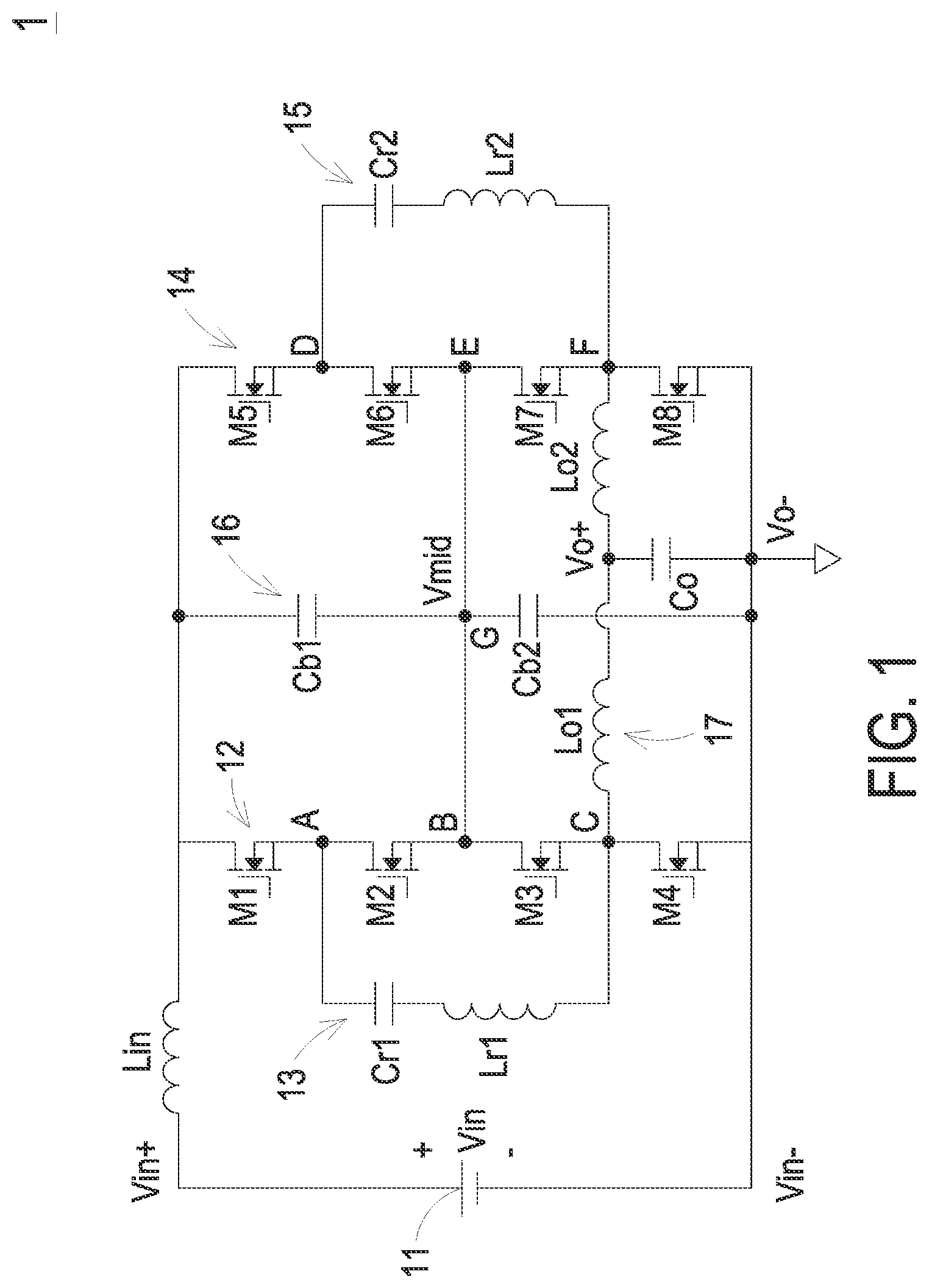
is a schematic circuit diagram illustrating a power conversion circuit according to a first embodiment of the present disclosure. In this embodiment, the power conversion circuit 1 is a resonant switch capacitor buck converter. The power conversion circuit 1 is electrically connected between a power source 11 and a load (not shown). The power conversion circuit 1 receives an input voltage Vin from the power source 11 . The input voltage Vin is converted into an output voltage Vo by the power conversion circuit 1 . The output voltage Vo is transmitted to the load. The power conversion circuit 1 includes an input positive terminal Vin+, an input negative terminal Vin−, an output positive terminal Vo+, an output negative terminal Vo−, an input inductor Lin, a first switch bridge arm 12 , a first resonant branch 13 , a second switch bridge arm 14 , a second resonant branch 15 , a capacitor branch 16 , an output inductor unit 17 and an output capacitor Co. The input positive terminal Vin+ and the input negative terminal Vin− are electrically connected with the two terminals of the voltage source 11 . The power conversion circuit 1 receives the input voltage Vin through the input positive terminal Vin+ and the input negative terminal Vin−. The output positive terminal Vo+ and the output negative terminal Vo− are electrically connected with the load. The output voltage Vo is outputted from the power conversion circuit 1 to the load through the output positive terminal Vo+ and the output negative terminal Vo−. The input negative terminal Vin− is electrically connected with the output negative terminal Vo−.
The first terminal of the input inductor Lin is electrically connected with the input positive terminal Vin+. The first switch bridge arm 12 is electrically connected between the second terminal of the input inductor Lin and the input negative terminal Vin−. The first switch bridge arm 12 includes a first switch M 1 , a second switch M 2 , a third switch M 3 and a fourth switch M 4 , which are sequentially connected in series. The first switch M 1 is electrically connected with the input positive terminal Vin+. The fourth switch M 4 is electrically connected with the input negative terminal Vin−. The first switch M 1 and the second switch M 2 are electrically connected with a first node A. The second switch M 2 and the third switch M 3 are electrically connected with a second node B. The third switch M 3 and the fourth switch M 4 is electrically connected with a third node C. Preferably but not exclusively, the switches M 1 , M 2 , M 3 and M 4 of the first switch bridge arm 12 are MOSFET switches, GaN switches, FET switches or IGBT switches.
The first resonant branch 13 is electrically connected between the first node A and the third node C. Moreover, the first resonant branch 13 includes a first resonant capacitor Cr 1 and a first resonant inductor Lr 1 , which are connected with each other in series.
The second switch bridge arm 14 is electrically connected between the second terminal of the input inductor Lin and the input negative terminal Vin−. The second switch bridge arm 14 includes a fifth switch M 5 , a sixth switch M 6 , a seventh switch M 7 and an eighth switch M 8 , which are sequentially connected in series. The fifth switch M 5 is electrically connected with the input positive terminal Vin+. The eighth switch M 8 is electrically connected with the input negative terminal Vin−. The fifth switch M 5 and the sixth switch M 6 are electrically connected with a fourth node D. The sixth switch M 6 and the seventh switch M 7 are electrically connected with a fifth node E. The seventh switch M 7 and the eighth switch M 8 are electrically connected with a sixth node F. Preferably but not exclusively, the switches M 5 , M 6 , M 7 and M 8 of the second switch bridge arm 14 are MOSFET switches, GaN switches, FET switches or IGBT switches.
The second resonant branch 15 is connected between the fourth node D and the sixth node F. Moreover, the second resonant branch 15 includes a second resonant capacitor Cr 2 and a second resonant inductor Lr 2 , which are connected with each other in series.
The capacitor branch 16 is connected with the first switch bridge arm 12 and the second switch bridge arm 14 in parallel. In this embodiment, the capacitor branch 16 is connected between the second terminal of the input inductor Lin and the input negative terminal Vin−. Moreover, the capacitor branch 16 includes a first half-bridge capacitor Cb 1 and a second half-bridge capacitor Cb 2 , which are electrically connected with each other. The first half-bridge capacitor Cb 1 and the second half-bridge capacitor Cb 2 are electrically connected with a seventh node G. Moreover, the seventh node G, the second node B and the fifth node E are directly connected with each other. The voltage at the seventh node G is equal to a midpoint voltage Vmid.
The output inductor unit 17 is electrically connected between the third node C and the sixth node F. Moreover, the output inductor unit 17 includes a first output inductor Lo 1 and a second output inductor Lo 2 . The first output inductor Lo 1 is electrically connected between the third node C and the output positive terminal Vo+. The second output inductor Lo 2 is electrically connected between the sixth node F and the output positive terminal Vo+.
The output capacitor Co is electrically connected between the output positive terminal Vo+ and the output negative terminal Vo−.
The power conversion circuit 1 further includes a control circuit (not shown). The control circuit issues driving signals to control the operations of the switches M 1 , M 2 , M 3 , M 4 , M 5 , M 6 , M 7 and M 8 . These driving signals are PWM signals. According to the driving signals, the power conversion circuit 1 is capable of converting the input voltage Vin into the output voltage Vo. The power conversion circuit 1 is a buck circuit. The operations of the power conversion circuit 1 will be described in more details as follows.
is a first exemplary timing waveform diagram illustrating voltages and currents of associated components in the power conversion circuit as shown in . In , Vgs_M 1 denotes the gate-source voltage of the first switch M 1 , Vgs_M 2 denotes the gate-source voltage of the second switch M 2 , Vgs_M 3 denotes the gate-source voltage of the third switch M 3 , Vgs_M 4 denotes the gate-source voltage of the fourth switch M 4 , Vgs_M 5 denotes the gate-source voltage of the fifth switch M 5 , Vgs_M 6 denotes the gate-source voltage of the sixth switch M 6 , Vgs_M 7 denotes the gate-source voltage of the seventh switch M 7 , and Vgs_M 8 denotes the gate-source voltage of the eighth switch M 8 . Moreover, iLr 1 denotes the current flowing through the first resonant inductor Lr 1 , and iLr 2 denotes the current flowing through the second resonant inductor Lr 2 .
As shown in , the time interval between the time point t=0 and the time point t 3 is equal to one switching cycle Ts. The first switch M 1 , the third switch M 3 and the sixth switch M 6 receives a first driving signal. For example, these switches M 1 , M 3 and M 6 are MOSFET switches. The first driving signal corresponds to the voltages Vgs_M 1 , Vgs_M 3 and Vgs_M 6 . Consequently, the one/off states of the switches M 1 , M 3 and M 6 are controlled according to the first driving signal. So that the first switch M 1 , the third switch M 3 and the sixth switch M 6 are turned on and turned off synchronously. The duty cycle (Duty) of the first driving signal is lower than or equal to 50%. That is, in any switching cycle, the on period of each of the switches M 1 , M 3 and M 6 is equal to Duty*Ts. The fourth switch M 4 receives a second driving signal. For example, the fourth switch M 4 is a MOSFET switch. The second driving signal corresponds to the voltages Vgs_M 4 . Consequently, the one/off states of the fourth switch M 4 are controlled according to the second driving signal. The first driving signal and the second driving signal are complementary to each other. Moreover, the duty cycle of the second driving signal is equal to (1−Duty). That is, in any switching cycle, the on period of the switch M 4 is equal to (1−Duty)*Ts. The second switch M 2 , the fifth switch M 5 and the seventh switch M 7 receive a third driving signal. For example, these switches M 2 , M 5 and M 7 are MOSFET switches. The third driving signal corresponds to the voltages Vgs_M 2 , Vgs_M 5 and Vgs_M 7 . Consequently, the one/off states of the switches M 2 , M 5 and M 7 are controlled according to the third driving signal. So that the second switch M 2 , the fifth switch M 5 and the seventh switch M 7 are turned on and turned off synchronously. The duty cycle (Duty) of the third driving signal is lower than or equal to 50%. That is, in any switching cycle, the on period of each of the switches M 2 , M 5 and M 7 is equal to Duty*Ts. In this embodiment, the phase difference between the third driving signal and the first driving signal is 180 degrees. The eighth switch M 8 receives a fourth driving signal. For example, the eighth switch M 8 is a MOSFET switch. The fourth driving signal corresponds to the voltages Vgs_M 8 . Consequently, the one/off states of the eighth switch M 8 are controlled according to the fourth driving signal. The third driving signal and the fourth driving signal are complementary to each other. Moreover, the duty cycle of the fourth driving signal is equal to (1−Duty). That is, in any switching cycle, the on period of the switch M 8 is equal to (1−Duty)*Ts.
Please refer to the control method of and the circuitry topology of . In the time interval between the time point t=0 and the time point t 0 , the first switch M 1 and the third witch M 3 are turned on. At this time, the first resonant branch 13 is electrically connected with the two terminals of the first half-bridge capacitor Cb 1 of the capacitor branch 16 in parallel. Consequently, the first resonant branch 13 is charged by the voltage of the first half-bridge capacitor Cb 1 of the capacitor branch 16 . Moreover, a forward resonance between the first resonant capacitor Cr 1 and the first resonant inductor Lr 1 of the first resonant branch 13 occurs. The current iLr 1 flowing through the first resonant inductor Lr 1 starts to rise from zero (i.e., in a positive rising manner). Since the third switch M 3 is turned on, the voltage difference between the two terminals of the first output inductor Lo 1 is equal to the voltage difference between the midpoint voltage Vmid (i.e., the terminal voltage of the second half-bridge capacitor Cb 2 ) and the output voltage Vo, i.e., Vmid−Vo. Consequently, the current flowing through the first output inductor Lo 1 of the output inductor unit 17 is increased.
At the time point t 0 , the current iLr 1 flowing through the first resonant inductor Lr 1 is forwardly decreased to be close to zero. Meanwhile, the first switch M 1 and the third switch M 3 are turned off, and the fourth switch M 4 is turned on. Consequently, through the freewheeling of the body diode of the second switch M 2 , the current iLr 1 flowing through the first resonant inductor Lr 1 is decreased to zero. When the current iLr 1 flowing through the first resonant inductor Lr 1 is equal to zero, the resonance between the first resonant capacitor Cr 1 and the first resonant inductor Lr 1 is stopped. Consequently, the current iLr 1 flowing through the first resonant inductor Lr 1 is maintained at zero. Since the fourth switch M 4 is turned on, the voltage difference between the two terminals of the first output inductor Lo 1 of the output inductor unit 17 is equal to −Vo. Consequently, the current flowing through the first output inductor Lo 1 of the output inductor unit 17 is decreased. In the time interval between the time point t 0 and the time point t 1 , the first switch M 1 and the third switch M 3 are turned off when the current iLr 1 flowing through the first resonant inductor Lr 1 is forwardly decreased to be close to zero or the current iLr 1 flowing through the first resonant inductor Lr 1 is forwardly decreased to zero. That is, the first switch M 1 and the third switch M 3 are turned off before the negative value of the current iLr 1 is generated.
In the time interval between the time point t 1 and the time point t 2 , the second switch M 2 and the fourth switch M 4 are turned on. At this time, the first resonant branch 13 is electrically connected with the two terminals of the second half-bridge capacitor Cb 2 of the capacitor branch 16 in parallel. Consequently, the second half-bridge capacitor Cb 2 of the capacitor branch 16 is discharged by the first resonant branch 13 . Moreover, a resonant between the first resonant capacitor Cr 1 and the first resonant inductor Lr 1 of the first resonant branch 13 occurs. Consequently, the current iLr 1 flowing through the first resonant inductor Lr 1 starts to drop from zero (i.e., in a reverse rising manner). Moreover, since the fourth switch M 4 is turned on, the current flowing through the first output inductor Lo 1 of the output inductor unit 17 is continuously decreased.
At the time point t 2 , the current iLr 1 flowing through the first resonant inductor Lr 1 is reversely decreased to be close to zero. Meanwhile, the second switch M 2 is turned off, and the fourth switch M 4 is turned on. Consequently, through the freewheeling of the body diode of the first switch M 1 , the current iLr 1 flowing through the first resonant inductor Lr 1 is decreased to zero. When the current iLr 1 flowing through the first resonant inductor Lr 1 is equal to zero, the resonance between the first resonant capacitor Cr 1 and the first resonant inductor Lr 1 is stopped. Consequently, the current iLr 1 flowing through the first resonant inductor Lr 1 is maintained at zero. Since the fourth switch M 4 is turned on, the voltage difference between the two terminals of the first output inductor Lo 1 of the output inductor unit 17 is equal to −Vo. The current flowing through the first output inductor Lo 1 of the output inductor unit 17 is continuously decreased. In the time interval between the time point t 2 and the time point t 3 , the second switch M 2 is turned off when the current iLr 1 flowing through the first resonant inductor Lr 1 is increased to be close to zero from negative value, or the current iLr 1 flowing through the first resonant inductor Lr 1 is increased to zero from negative value. That is, the second switch M 2 is turned off before the positive value of the current iLr 1 of the first resonant inductor Lr 1 is generated.
After the time point t 3 , the fourth switch M 4 is turned off, and the first switch M 1 and the third switch M 3 are turned on. Consequently, the new switching cycle is repeated.
As mentioned above, the current iLr 1 flowing through the first resonant inductor Lr 1 is controlled according to the switching sequence of the first switch M 1 , the second switch M 2 , the third switch M 3 and the fourth switch M 4 . Similarly, the current iLr 2 flowing through the second resonant inductor Lr 2 is controlled according to the switching sequence of the fifth switch M 5 , the sixth switch M 6 , the seventh switch M 7 and the eighth switch M 8 . The method of controlling the current iLr 2 and the method of controlling the current iLr 1 are in a duality relation.
In the time interval between the time point t=0 and the time point t 0 , the sixth switch M 6 and the eighth switch M 8 are turned on. At this time, the second resonant branch 15 is electrically connected with the two terminals of the second half-bridge capacitor Cb 2 of the capacitor branch 16 in parallel. Moreover, a reverse resonance between the second resonant capacitor Cr 2 and the second resonant inductor Lr 2 of the second resonant branch 15 occurs. The current iLr 2 flowing through the second resonant inductor Lr 2 starts to drop from zero (i.e., in a reverse rising manner).
In the time interval between the time point t 1 and the time point t 2 , the fifth switch M 5 and the seventh switch M 7 are turned on. At this time, the second resonant branch 15 is electrically connected with the two terminals of the first half-bridge capacitor Cb 1 of the capacitor branch 16 in parallel. Moreover, a forward resonance between the second resonant capacitor Cr 2 and the second resonant inductor Lr 2 of the second resonant branch 15 occurs. The current iLr 2 flowing through the second resonant inductor Lr 2 starts to rise from zero (i.e., in a positive rising manner). The control method and operating principle of the second resonant branch 15 are similar to those of the first resonant branch 13 , and not redundantly described herein.
Please refer to the circuitry topology of the power conversion circuit 1 as shown in and the waveform diagram as shown in . During the operations of the power conversion circuit 1 , the current iLr 1 flowing through the first resonant inductor Lr 1 and the current iLr 2 flowing through the second resonant inductor Lr 2 are discontinuous, and the duty cycle Duty is lower than or equal to 50%. The magnitude of the input voltage Vin is decreased to the midpoint voltage Vmid (i.e., the voltage at the seventh node G). Consequently, the midpoint voltage Vmid is equal to 0.5×Vin, and the output voltage Vo is equal to Vmid×Duty (or 0.5×Vin×Duty). That is, the magnitude of the output voltage Vo is lower than or equal to 0.25×Vin. Consequently, the voltage reduction efficacy of the power conversion circuit 1 is enhanced.
As mentioned above, the power conversion circuit 1 includes the first resonant inductor Lr 1 and the second resonant inductor Lr 2 . The branch current of the first resonant branch 13 and the branch current of the second resonant branch 15 start to rise from zero in the forward or reverse direction. Consequently, the purposes of turning on the first switch M 1 and the second switch M 2 of the first switch bridge arm 12 under the zero current condition are achieved, and the purposes of turning on the fifth switch M 5 and the sixth switch M 6 of the second switch bridge arm 14 under the zero current condition are achieved. In this way, the turn-on loss of the first switch bridge arm 12 and the second switch bridge arm 14 will be reduced.
When the amplitude of the current flowing through the first resonant branch 13 is decreased to be close to zero, the first switch M 1 or the second switch M 2 is turned off. Moreover, when the amplitude of the current flowing through the second resonant branch 15 is decreased to be close to zero, the fifth switch M 5 or the sixth switch M 6 is turned off. Consequently, the purposes of turning off the first switch M 1 and the second switch M 2 of the first switch bridge arm 12 under the zero current condition are achieved, and the purposes of turning off the fifth switch M 5 and the sixth switch M 6 of the second switch bridge arm 14 under the zero current condition are achieved. In this way, the turn-off loss of the first switch bridge arm 12 and the second switch bridge arm 14 will be reduced.
As mentioned above, the first resonant branch 13 includes the first resonant inductor Lr 1 . Consequently, the capacitors with high capacitance can be used as the first half-bridge capacitor Cb 1 and the second half-bridge capacitor Cb 2 . In addition, the first resonant branch 13 will not generate the inrush current when the on/off states of the switches are changed. Since the first half-bridge capacitor Cb 1 and the second half-bridge capacitor Cb 2 have the large capacitance, the first half-bridge capacitor Cb 1 and the second half-bridge capacitor Cb 2 can effectively provide the voltage clamping function to the first switch M 1 , the second switch M 2 , the third switch M 3 and the fourth switch M 4 . Similarly, the second resonant branch 15 includes the second resonant inductor Lr 2 . Consequently, the capacitors with high capacitance can be used as the first half-bridge capacitor Cb 1 and the second half-bridge capacitor Cb 2 . In addition, the second resonant branch 15 will not generate the inrush current when the on/off states of the switches are changed. Since the first half-bridge capacitor Cb 1 and the second half-bridge capacitor Cb 2 have the large capacitance, the first half-bridge capacitor Cb 1 and the second half-bridge capacitor Cb 2 can effectively provide the voltage clamping function to the fifth switch M 5 , a sixth switch M 6 , a seventh switch M 7 and an eighth switch M 8 . Consequently, the switches with the low rated voltages can be used as the switches of the first switch bridge arm 12 and the switches of the second switch bridge arm 14 . Since the conduction loss of the switches is reduced, the power loss of the power conversion circuit 1 is reduced, and the efficiency is enhanced.
The control method of the power conversion circuit 1 may be modified. In some embodiments, the purpose of increasing the output voltage is achieved by adjusting the duty cycle and the switching sequence.
is a second exemplary timing waveform diagram illustrating voltages and currents of associated components in the power conversion circuit as shown in . As shown in , the time interval between the time point t=0 and the time point t 3 is equal to one switching cycle Ts. The third switch M 3 receives a first driving signal. For example, the third switch M 3 is a MOSFET switch. The first driving signal corresponds to the voltage Vgs_M 3 . Consequently, the on/off states of the third switch M 3 are controlled according to the first driving signal. The duty cycle (Duty) of the first driving signal is higher than 50%. That is, in any switching cycle, the on period of the third switch M 3 is equal to Duty*Ts. The second switch M 2 , the fourth switch M 4 and the fifth switch M 5 receive a second driving signal. For example, the second switch M 2 , the fourth switch M 4 and the fifth switch M 5 are MOSFET switches. The second driving signal corresponds to the voltages Vgs_M 2 , Vgs_M 4 and Vgs_M 5 . Consequently, the on/off states of the switches M 2 , M 4 and M 5 are controlled according to the second driving signal. So that the second switch M 2 , the fourth switch M 4 and the fifth switch M 5 are turned on and turned off synchronously. The first driving signal and the second driving signal are complementary to each other. Moreover, the duty cycle of the second driving signal is equal to (1−Duty). That is, in any switching cycle, the on period of each of the switches M 2 , M 4 and M 5 is equal to (1−Duty)*Ts. The seventh switch M 7 receives a third driving signal. For example, the seventh switch M 7 is a MOSFET switch. The third driving signal corresponds to the voltage Vgs_M 7 . Consequently, the on/off states of the seventh switch M 7 are controlled according to the third driving signal. The duty cycle (Duty) of the third driving signal is higher than 50%. That is, in any switching cycle, the on period of the seventh switch M 7 is equal to Duty*Ts. The first switch M 1 , the sixth switch M 6 and eighth switch M 8 receive a fourth driving signal. For example, the first switch M 1 , the sixth switch M 6 and eighth switch M 8 are MOSFET switches. The fourth driving signal corresponds to the voltages Vgs_M 1 , Vgs_M 6 and Vgs_M 8 . Consequently, the on/off states of the switches M 1 , M 6 and M 8 are controlled according to the fourth driving signal. So that the first switch M 1 , the sixth switch M 6 and eighth switch M 8 are turned on and turned off synchronously. The third driving signal and the fourth driving signal are complementary to each other. Moreover, the duty cycle of the fourth driving signal is equal to (1−Duty). That is, in any switching cycle, the on period of each of the switches M 1 , M 6 and M 8 is equal to (1−Duty)*Ts. In this embodiment, the phase difference between the fourth driving signal and the second driving signal is 180 degrees.
The control method of is similar to the control method of . When both of the first switch M 1 and the third switch M 3 are turned on (e.g., in the time interval between the time point t 0 and the time point t 1 ), the first resonant branch 13 is charged by the voltage of the first half-bridge capacitor Cb 1 of the capacitor branch 16 . Moreover, a forward resonance between the first resonant capacitor Cr 1 and the first resonant inductor Lr 1 of the first resonant branch 13 occurs. The current iLr 1 flowing through the first resonant inductor Lr 1 starts to rise from zero to the peak value and then drops. When the current iLr 1 is decreased to be close to zero, the first switch M 1 is turned off. Meanwhile, the resonance between the first resonant capacitor Cr 1 and the first resonant inductor Lr 1 is stopped. Consequently, the current iLr 1 flowing through the first resonant inductor Lr 1 is maintained at zero.
When the third switch M 3 is turned on (e.g., in the time interval between the time point t 0 and the time point t 2 ), the first output inductor Lo 1 of the output inductor 17 extracts the current of the second half-bridge capacitor Cb 2 through the third switch M 3 . When the third switch M 3 is turned off and both of the second switch M 2 and the fourth switch M 4 are turned on (e.g., in the time interval between the time point t 2 and the time point t 3 ), the first output inductor Lo 1 of the output inductor unit 17 freewheels through the fourth transistor M 4 . The second half-bridge capacitor Cb 2 of the capacitor branch 16 is discharged by the first resonant branch 13 . Moreover, a reverse resonance between the first resonant capacitor Cr 1 and the first resonant inductor Lr 1 of the first resonant branch 13 occurs. The current iLr 1 flowing through the first resonant inductor Lr 1 starts to drop from zero to the negative peak value and then rises. When the current iLr 1 is increased to be close zero (e.g., in the time interval between the time point t 3 and the time point t 4 ), both of the second switch M 2 and the fourth switch M 4 are turned off and the third switch M 3 is turned on. Meanwhile, the first output inductor Lo 1 of the output inductor unit 17 extracts the current of the second half-bridge capacitor Cb 2 through the third switch M 3 .
Then, a new switching cycle is repeated. The procedure of the new switching cycle will not be redundantly described herein. As mentioned above, the current iLr 1 flowing through the first resonant inductor Lr 1 is controlled according to the switching sequence of the first switch M 1 , the second switch M 2 , the third switch M 3 and the fourth switch M 4 . Similarly, the current iLr 2 flowing through the second resonant inductor Lr 2 is controlled according to the switching sequence of controlling the fifth switch M 5 , the sixth switch M 6 , the seventh switch M 7 and the eighth switch M 8 . The method of controlling the current iLr 2 and the method of controlling the current iLr 1 are in a duality relation.
Please refer to the circuitry topology of the power conversion circuit 1 as shown in and the waveform diagram as shown in . During the operations of the power conversion circuit 1 , the current iLr 1 flowing through the first resonant inductor Lr 1 and the current iLr 2 flowing through the second resonant inductor Lr 2 are discontinuous, and the duty cycle (Duty) is lower than or equal to 50%. The magnitude of the input voltage Vin is decreased to the midpoint voltage Vmid (i.e., the voltage at the seventh node G). Consequently, the midpoint voltage Vmid is equal to 0.5×Vin, and the output voltage Vo is equal to Vmid×Duty (or 0.5×Vin×Duty). That is, the magnitude of the output voltage Vo is higher than 0.25×Vin. Since the magnitude of the output voltage Vo can be lower than or equal to 0.25×Vin or the magnitude of the output voltage Vo can be higher than 0.25×Vin, the output voltage range of the power conversion circuit 1 is widened.
As mentioned above, the power conversion circuit 1 includes the first resonant inductor Lr 1 and the second resonant inductor Lr 2 . The branch current of the first resonant branch 13 and the branch current of the second resonant branch 15 start to rise from zero in the forward or reverse direction. When the amplitude of the current flowing through the first resonant branch 13 is decreased to zero, the first switch M 1 or the second switch M 2 is turned off. Moreover, when the amplitude of the current flowing through the second resonant branch 15 is decreased to zero, the fifth switch M 5 or the sixth switch M 6 is turned off. Consequently, the purposes of turning on the first switch M 1 and the second switch M 2 of the first switch bridge arm 12 under the zero current condition are achieved, the purposes of turning off the first switch M 1 and the second switch M 2 of the first switch bridge arm 12 under the zero current condition are achieved, the purposes of turning on the fifth switch M 5 and the sixth switch M 6 of the second switch bridge arm 14 under the zero current condition are achieved, and the purposes of turning off the fifth switch M 5 and the sixth switch M 6 of the second switch bridge arm 14 under the zero current condition are achieved. In this way, the turn-on loss and the turn-off loss of the first switch bridge arm 12 and the second switch bridge arm 14 will be reduced.
When the control method of and the control method of are applied to the power conversion circuit 1 of , two voltage reduction approaches can be achieved. In the first voltage reduction approach, the magnitude of the output voltage Vo is lower than or equal to 0.25×Vin. In the second voltage reduction approach, the magnitude of the output voltage Vo is higher than 0.25×Vin. Consequently, the range of the gain (i.e., the ratio of the output voltage Vo to the input voltage Vin) of the power conversion circuit 1 is wide. Moreover, even if the range of the input voltage Vin is wider, the output voltage Vo is still stabilized. For example, in case that the input voltage Vin is in the range between 40V and 60V and the output voltage Vo is 12V, the duty cycle (Duty) can be in the range between 0.4 and 0.6. Moreover, in case that the input voltage Vin is in the range between 36V and 75V and the output voltage Vo is 12V, the duty cycle (Duty) can be in the range between 0.32 and 0.67.
In the embodiments of and , the current iLr 1 flowing through the first resonant inductor Lr 1 and the current iLr 2 flowing through the second resonant inductor Lr 2 are discontinuous during the operations of the power conversion circuit 1 . In some embodiments, the current iLr 1 flowing through the first resonant inductor Lr 1 and the current iLr 2 flowing through the second resonant inductor Lr 2 are continuous.
is a third exemplary timing waveform diagram illustrating voltages and currents of associated components in the power conversion circuit as shown in . As shown in , the time interval between the time point t=0 and the time point t 3 is equal to on switching cycle Ts. The first switch M 1 and third switch M 3 receive a first driving signal. For example, the first switch M 1 and third switch M 3 are MOSFET switches. The first driving signal corresponds to the voltages Vgs_M 1 and Vgs_M 3 . Consequently, the on/off states of the switches M 1 and M 3 are controlled according to the first driving signal. So that the first switch M 1 and third switch M 3 are turned on and turned off synchronously. The first driving signal has a duty cycle (Duty). That is, the on period of each of the switches M 1 and M 3 is equal to Duty*Ts. The second switch M 2 and the fourth switch M 4 receive the second driving signal. For example, the second switch M 2 and the fourth switch M 4 are MOSFET switches. The second driving signal corresponds to the voltages Vgs_M 2 and Vgs_M 4 . Consequently, the on/off states of the switches M 2 and M 4 are controlled according to the second driving signal. So that the second switch M 2 and the fourth switch M 4 are turned on and turned off synchronously. Moreover, the duty cycle of the second driving signal is equal to (1−Duty). That is, in any switching cycle, the on period of each of the switches M 2 and M 4 is equal to (1−Duty)*Ts. The first driving signal and the second driving signal are complementary to each other. The fifth switch M 5 and the seventh switch M 7 receive a third driving signal. For example, the switches M 5 and M 7 are MOSFET switches. The third driving signal corresponds to the voltages Vgs_M 5 and Vgs_M 7 . Consequently, the on/off states of the switches M 5 and M 7 are controlled according to the third driving signal. So that the fifth switch M 5 and the seventh switch M 7 are turned on and turned off synchronously. The third driving signal has the duty cycle (Duty). That is, in any switching cycle, the on period of each of the switches M 5 and M 7 is equal to Duty*Ts. In this embodiment, the phase difference between the third driving signal and the first driving signal is 180 degrees. The sixth switch M 6 and eighth switch M 8 receive a fourth driving signal. For example, the sixth switch M 6 and eighth switch M 8 are MOSFET switches. The fourth driving signal corresponds to the Vgs_M 6 and Vgs_M 8 . Consequently, the on/off states of the switches M 6 and M 8 are controlled according to the fourth driving signal. So that the sixth switch M 6 and eighth switch M 8 are turned on and turned off synchronously. Moreover, the duty cycle of the fourth driving signal is equal to (1−Duty). That is, in any switching cycle, the on period of each of the switches M 6 and M 8 is equal to (1−Duty)*Ts. Moreover, the third driving signal and the fourth driving signal are complementary to each other.
The control method as shown in is similar to the control method as shown in . When the first switch M 1 and the third switch M 3 are turned on, the first resonant branch 13 is charged by the voltage of the first half-bridge capacitor Cb 1 of the capacitor branch 16 . Moreover, a forward resonance between the first resonant capacitor Cr 1 and the first resonant inductor Lr 1 of the first resonant branch 13 occurs. The current iLr 1 flowing through the first resonant inductor Lr 1 starts to rise from zero to the positive peak and then drops. When the on period Duty*Ts is ended (i.e., at the time point t 2 ), the first switch M 1 and the third switch M 3 are turned off, and the second switch M 2 and the fourth switch M 4 are turned on. Meanwhile, the resonant current of the first resonant capacitor Cr 1 and the first resonant inductor Lr 1 continuously drops to zero through the second switch M 2 and the fourth switch M 4 . Then, the reverse resonance occurs.
When the third switch M 3 is turned on, the first output inductor Lo 1 of the output inductor unit 17 extracts the current of the second half-bridge capacitor Cb 2 through the third switch M 3 . When the first switch M 1 and the third switch M 3 are turned off and the second switch M 2 and the fourth switch M 4 are turned on, the first output inductor Lo 1 of the output inductor unit 17 freewheels through the fourth switch M 4 . The second half-bridge capacitor Cb 2 of the capacitor branch 16 is discharged by the first resonant branch 13 . Moreover, a reverse resonance between the first resonant capacitor Cr 1 and the first resonant inductor Lr 1 of the first resonant branch 13 occurs. The current iLr 1 flowing through the first resonant inductor Lr 1 starts to drop from zero to the negative peak value and then rises. When the current iLr 1 is increased to be close zero (e.g., in the time interval between the time point t 3 and the time point t 4 ), both of the second switch M 2 and the fourth switch M 4 are turned off, and the first switch M 1 and the third switch M 3 are turned on.
Then, a new switching cycle is repeated. The procedure of the new switching cycle will not be redundantly described herein. As mentioned above, the current iLr 1 flowing through the first resonant inductor Lr 1 is controlled according to the switching sequence of the first switch M 1 , the second switch M 2 , the third switch M 3 and the fourth switch M 4 . Similarly, the current iLr 2 flowing through the second resonant inductor Lr 2 is controlled according to the switching sequence of controlling the fifth switch M 5 , the sixth switch M 6 , the seventh switch M 7 and the eighth switch M 8 . The method of controlling the current iLr 2 and the method of controlling the current iLr 1 are in a duality relation.
Please refer to the circuitry topology of the power conversion circuit 1 as shown in and the waveform diagram as shown in . The midpoint voltage Vmid is still equal to 0.5×Vin, and the output voltage Vo is equal to Vmid×Duty (or 0.5×Vin×Duty). During the operations of the power conversion circuit 1 , the current iLr 1 flowing through the first resonant inductor Lr 1 and the current iLr 2 flowing through the second resonant inductor Lr 2 are continuous. When compared with the discontinuous currents iLr 1 and iLr 2 of and , the current effective values of the first switch bridge arm 12 and the second switch bridge arm 14 in this embodiment will be decreased, and the turn-on loss of the first switch bridge arm 12 and the second switch bridge arm 14 will be reduced. When the current iLr 1 flowing through the first resonant inductor Lr 1 is increased to be close to zero, the switching cycle is equal to the resonant cycle of the first resonant capacitor Cr 1 and the first resonant inductor Lr 1 by the controlling method of turning off the second switch M 2 and the fourth switch M 4 . Consequently, the purpose of turning off the second switch M 2 under the zero current condition and the purpose of turning on the first switch M 1 are achieved.
In some embodiments, the power conversion circuit includes a single switch bridge arm, a single resonant branch and a single capacitor branch to control the current of a single output inductor. is a schematic circuit diagram illustrating a power conversion circuit according to a second embodiment of the present disclosure. The circuitry topology of the power conversion circuit 1 a of this embodiment is similar to that of the power conversion circuit 1 as shown in . In this embodiment, the power conversion circuit 1 a includes an input positive terminal Vin+, an input negative terminal Vin−, an output positive terminal Vo+, an output negative terminal Vo−, an input inductor Lin, a first switch bridge arm 12 , a first resonant branch 13 , a capacitor branch 16 , an output inductor unit 17 and an output capacitor Co. In comparison with , the power conversion circuit 1 a of this embodiment omits the second switch bridge arm bridge 14 and the second resonant branch 15 . The output inductor unit 17 of the power conversion circuit 1 a of this embodiment includes a first output inductor Lo 1 only. That is, the output inductor unit 17 of the power conversion circuit 1 a omits the second output inductor Lo 2 . The other components of the power conversion circuit 1 a of this embodiment are similar to those of the power conversion circuit 1 , and not redundantly described herein.
is a schematic timing waveform diagram illustrating voltages and currents of associated components in the power conversion circuit as shown in . In , Vgs_M 1 denotes the gate-source voltage of the first switch M 1 , Vgs_M 2 denotes the gate-source voltage of the second switch M 2 , Vgs_M 3 denotes the gate-source voltage of the third switch M 3 , and Vgs_M 4 denotes the gate-source voltage of the fourth switch M 4 . Moreover, iLr 1 denotes the current flowing through the first resonant inductor Lr 1 .
As shown in , the time interval between the time point t=0 and the time point t 3 is equal to on switching cycle Ts. The first switch M 1 and third switch M 3 receive a first driving signal. For example, the first switch M 1 and third switch M 3 are MOSFET switches. The first driving signal corresponds to the voltages Vgs_M 1 and Vgs_M 3 . Consequently, the on/off states of the switches M 1 and M 3 are controlled according to the first driving signal. So that the first switch M 1 and the third switch M 3 are turned on and turned off synchronously. The duty cycle (Duty) of the first driving signal is lower than or equal to 50%. That is, in any switching cycle, the on period of each of the switches M 1 and M 3 is equal to Duty*Ts. The fourth switch M 4 receives a second driving signal. For example, the fourth switch M 4 is a MOSFET switch. The second driving signal corresponds to the voltage Vgs_M 4 . Consequently, the on/off states of the switch M 4 are controlled according to the second driving signal. The first driving signal and the second driving signal are complementary to each other. Moreover, the duty cycle of the second driving signal is equal to (1−Duty). That is, in any switching cycle, the on period of the fourth switch M 4 is equal to (1−Duty)*Ts. The second switch M 2 receives a third driving signal. For example, the second switch M 2 is a MOSFET switch. The third driving signal corresponds to the voltage Vgs_M 2 . Consequently, the on/off states of the second switch M 2 are controlled according to the third driving signal. The duty cycle (Duty) of the third driving signal is lower than or equal to 50%. That is, in any switching cycle, the on period of the second switch M 2 is equal to Duty*Ts. In this embodiment, the phase difference between the third driving signal and the first driving signal is 180 degrees.
Please refer to the control method of and the circuitry topology of . In the time interval between the time point t=0 and the time point t 0 , the first switch M 1 and the third witch M 3 are turned on. At this time, the first resonant branch 13 is electrically connected in parallel with the two terminals of the first half-bridge capacitor Cb 1 of the capacitor branch 16 . Consequently, the first resonant branch 13 is charged by the voltage of the first half-bridge capacitor Cb 1 of the capacitor branch 16 . Moreover, a forward resonance between the first resonant capacitor Cr 1 and the first resonant inductor Lr 1 of the first resonant branch 13 occurs. The current iLr 1 flowing through the first resonant inductor Lr 1 starts to rise from zero (i.e., in a positive rising manner). Since the third switch M 3 is turned on, the voltage difference between the two terminals of the first output inductor Lo 1 is equal to the voltage difference between the midpoint voltage Vmid (i.e., the terminal voltage of the second half-bridge capacitor Cb 2 ) and the output voltage Vo, i.e., Vmid−Vo. Consequently, the current flowing through the first output inductor Lo 1 of the output inductor unit 17 increases.
At the time point t 0 , the current iLr 1 flowing through the first resonant inductor Lr 1 is forwardly decreased to be close to zero. Meanwhile, both of the first switch M 1 and the third switch M 3 are turned off, and the fourth switch M 4 is turned on. Consequently, through the freewheeling of the body diode of the second switch M 2 , the current iLr 1 flowing through the first resonant inductor Lr 1 is decreased to zero. When the current iLr 1 flowing through the first resonant inductor Lr 1 is equal to zero, the resonance between the first resonant capacitor Cr 1 and the first resonant inductor Lr 1 is stopped. Consequently, the current iLr 1 flowing through the first resonant inductor Lr 1 is maintained at zero. Since the fourth switch M 4 is turned on, the voltage difference between the two terminals of the first output inductor Lo 1 of the output inductor unit 17 is equal to −Vo. Consequently, the current flowing through the first output inductor Lo 1 of the output inductor unit 17 decreases. In the time interval between the time point t 0 and the time point t 1 , the first switch M 1 and the third switch M 3 are turned off when the current iLr 1 flowing through the first resonant inductor Lr 1 is forwardly decreased to be close to zero or the current iLr 1 flowing through the first resonant inductor Lr 1 is forwardly decreased to zero. That is, the first switch M 1 and the third switch M 3 are turned off before the negative current iLr 1 is generated.
In the time interval between the time point t 1 and the time point t 2 , the second switch M 2 and the fourth switch M 4 are turned on. Meanwhile, the first resonant branch 13 is electrically connected with the two terminals of the second half-bridge capacitor Cb 2 of the capacitor branch 16 in parallel. Consequently, the second half-bridge capacitor Cb 2 of the capacitor branch 16 is discharged by the first resonant branch 13 . Moreover, a resonance between the first resonant capacitor Cr 1 and the first resonant inductor Lr 1 of the first resonant branch 13 occurs. Consequently, the current iLr 1 flowing through the first resonant inductor Lr 1 starts to drop from zero (i.e., in a reverse rising manner). Moreover, since the fourth switch M 4 is turned on, the current flowing through the first output inductor Lo 1 of the output inductor unit 17 is continuously decreased.
At the time point t 2 , the current iLr 1 flowing through the first resonant inductor Lr 1 is reversely decreased to be close to zero. Meanwhile, the second switch M 2 is turned off and the fourth switch M 4 is turned on. Consequently, through the freewheeling of the body diode of the first switch M 1 , the current iLr 1 flowing through the first resonant inductor Lr 1 is decreased to zero. When the current iLr 1 flowing through the first resonant inductor Lr 1 is equal to zero, the resonance between the first resonant capacitor Cr 1 and the first resonant inductor Lr 1 is stopped. Consequently, the current iLr 1 flowing through the first resonant inductor Lr 1 is maintained at zero. Since the fourth switch M 4 is turned on, the voltage difference between the two terminals of the first output inductor Lo 1 of the output inductor unit 17 is equal to −Vo. The current flowing through the first output inductor Lo 1 of the output inductor unit 17 is continuously decreased.
In the time interval between the time point t 2 and the time point t 3 , the second switch M 2 is turned off when the current iLr 1 flowing through the first resonant inductor Lr 1 is forwardly increased to be close to zero or the current iLr 1 flowing through the first resonant inductor Lr 1 is forwardly increased to zero. That is, the second switch M 2 is turned off before the positive current iLr 1 of the first resonant inductor Lr 1 is generated.
After the time point t 3 , the fourth switch M 4 is turned off, and the first switch M 1 and the third switch M 3 are turned on. Then, a new switching cycle is repeated. The procedure of the new switching cycle will not be redundantly described herein.
By using the above control method, the current flowing through the first output inductor can be controlled. Consequently, the voltage reduction efficacy of the power conversion circuit 1 a is enhanced. Under this circumstance, the switches with the low rated voltages can be used. Since the conduction loss of the switches is reduced, the power loss of the power conversion circuit 1 a is reduced, and the efficiency is enhanced. It is noted that the control method for the power conversion circuit 1 a is not restricted. For example, the control method of or the control method of can be applied to the power conversion circuit 1 a.
For improving the performance of the power conversion circuit, a plurality of output inductors can be coupled with each other to form a coupled inductor, and a single magnetic device is used as the coupled inductor. Consequently, the core loss is reduced, the equivalent steady-state inductance is increased, and the equivalent dynamic inductance is reduced.
is a schematic circuit diagram illustrating a power conversion circuit according to a third embodiment of the present disclosure. The circuitry topology of the power conversion circuit 1 b of this embodiment is similar to that of the power conversion circuit 1 as shown in . In comparison with the power conversion circuit 1 , the first output inductor Lo 1 and the second output inductor Lo 2 in the power conversion circuit 1 b of this embodiment are coupled as a coupled inductor. In addition, the phase difference between the voltage at the third node C and the voltage at the sixth node F is 180 degrees. The voltage at the third node C is applied to the input terminal of the first output inductor Lo 1 . The voltage at the sixth node F is applied to the input terminal of the second output inductor Lo 2 . Consequently, the core loss is reduced, the equivalent steady-state inductance is increased, and the equivalent dynamic inductance is reduced.
The structure of the magnetic device as the coupled inductor of the power conversion circuit 1 b will be described as follows.
is a schematic exploded view illustrating a portion of a magnetic device of the power conversion circuit as shown in . schematically illustrates the magnetic device and associated switches of the power conversion circuit as shown in , in which the first magnetic cover is not shown. The magnetic device 2 is used as the coupled inductor of the power conversion circuit 1 b . For succinctness, the winding assembly of the magnetic device 2 is not shown in , and the first magnetic cover is not shown in .
As shown in , the magnetic device 2 includes a first magnetic cover 21 , a second magnetic cover 22 , a first magnetic leg 23 , a second magnetic leg 24 , a third magnetic leg 25 , a fourth magnetic leg 26 , a fifth magnetic leg 27 , a first winding 28 and a second winding 29 . The first magnetic cover 21 and the second magnetic cover 22 are opposed to each other. The first magnetic leg 23 , the second magnetic leg 24 , the third magnetic leg 25 , the fourth magnetic leg 26 and the fifth magnetic leg 27 are arranged between the first magnetic cover 21 and the second magnetic cover 22 . The first magnetic leg 23 and the third magnetic leg 25 are respectively arranged on the two opposite sides of the magnetic device 2 . The second magnetic leg 24 and the fourth magnetic leg 26 are respectively arranged on the other two opposed sides of the magnetic device 2 . Moreover, the first magnetic leg 23 and the third magnetic leg 25 are arranged between the second magnetic leg 24 and the fourth magnetic leg 26 . In addition, the first magnetic leg 23 , the second magnetic leg 24 , the third magnetic leg 25 , the fourth magnetic leg 26 are arranged around the fifth magnetic leg 27 .
Please refer to . The input terminal of the first winding 28 is connected with the third node C (i.e., the drain terminal of the fourth switch M 4 ). In addition, the input terminal of the first winding 28 is located beside the first magnetic leg 23 and the fourth magnetic leg 26 . The output terminal of the first winding 28 is connected with the output positive terminal Vo+. In addition, the output terminal of the first winding 28 is located beside the third magnetic leg 25 and the fourth magnetic leg 26 . The first winding 28 is sequentially transported through the region between the first magnetic leg 23 and the fourth magnetic leg 26 , the region between the first magnetic leg 23 and the fifth magnetic leg 27 , the region between the fifth magnetic leg 27 and the second magnetic leg 24 , the region between the fifth magnetic leg 27 and the third magnetic leg 25 and the region between the third magnetic leg 25 and the fourth magnetic leg 26 from the input terminal to the output terminal.
The input terminal of the second winding 29 is connected with the sixth node F (that is, the drain terminal of the eighth switch M 8 ). In addition, the input terminal of the second winding 29 is located beside the first magnetic leg 23 and the second magnetic leg 24 . The output terminal of the second winding 29 is connected with the output positive terminal Vo+. In addition, the output terminal of the second winding 29 is located beside the second magnetic leg 24 and the third magnetic leg 25 . The second winding 29 is sequentially transported through the region between the first magnetic leg 23 and the second magnetic leg 24 , the region between the first magnetic leg 23 and the fifth magnetic leg 27 , the region between the fifth magnetic leg 27 and the fourth magnetic leg 26 , the region between the fifth magnetic leg 27 and the third magnetic leg 25 and the region between the third magnetic leg 25 and the second magnetic leg 24 from the input terminal to the output terminal. The output negative terminal Vo− is connected with the source terminal of the fourth switch M 4 and the source terminal of the eighth switch M 8 .
In case that the direction of the current flowing through the first winding 28 and the direction of the current flowing through the second winding 29 are identical, the DC current in the first winding 28 flows from the input terminal of the first winding 28 to the output terminal of the first winding 28 , and the DC current in the second winding 29 flows from the input terminal of the second winding 29 to the output terminal of the second winding 29 .
In an embodiment, each of the second magnetic leg 24 and the fourth magnetic leg 26 has an air gap or a larger air gap, and each of the first magnetic leg 23 , the third magnetic leg 25 and the fifth magnetic leg 27 has no air gap or has a smaller air gap. In an embodiment, the magnetic resistance of the second magnetic leg 24 and the magnetic resistance of the fourth magnetic leg 26 are nearly equal. The magnetic resistance of each of the second magnetic leg 24 and the fourth magnetic leg 26 is larger than three times the magnetic resistance of each of the first magnetic leg 23 , the third magnetic leg 25 and the fifth magnetic leg 27 . The magnetic resistance of the first magnetic leg 23 and the magnetic resistance of the third magnetic leg 25 are nearly equal. The magnetic resistance of each of the first magnetic leg 23 and the third magnetic leg 25 is nearly equal to two times the magnetic resistance of the fifth magnetic leg 27 .
A first voltage is formed between the input terminal and the output terminal of the first winding 28 . A second voltage is formed between the input terminal and the output terminal of the second winding 29 . Moreover, the phase difference between the first voltage and the second voltage is 180 degrees. A half of the AC magnetic flux generated by the first winding 28 and a half of magnetic flux generated by the second winding 29 are cancelled out and transferred through the fifth magnetic leg 27 . The AC magnetic flux passing through the fifth magnetic leg 27 is evenly distributed to the first magnetic leg 23 and the third magnetic leg 25 . The directions of the AC magnetic fluxes passing through the first magnetic leg 23 and the third magnetic leg 25 are opposite to the direction of the AC magnetic flux passing through the fifth magnetic leg 27 . Consequently, the AC magnetic fluxes passing through the first magnetic leg 23 , the third magnetic leg 25 and the fifth magnetic leg 27 are large, but the DC magnetic fluxes are zero. A half of the AC magnetic flux generated by the first winding 28 and a half of magnetic flux generated by the second winding 29 are superposed and transferred through the second magnetic leg 24 and the fourth magnetic leg 26 . The direction of the AC magnetic flux passing through the second magnetic leg 24 and the direction of the AC magnetic flux passing through the fourth magnetic leg 26 are opposite. Consequently, the DC magnetic fluxes passing the second magnetic leg 24 and the fourth magnetic leg 26 are large, but the AC magnetic fluxes are small.
As mentioned above, the AC magnetic flux passing through the fifth magnetic leg 27 is large, but the air gap and the magnetic resistance of the fifth magnetic leg 27 are small. When compared with the fifth magnetic leg 27 , the air gap and the magnetic resistance of the second magnetic leg 24 are larger. Since the AC magnetic flux passing through the second magnetic leg 24 is smaller, the ripple of the AC current of the first winding 28 is lower. Similarly, the AC magnetic flux passing through the fifth magnetic leg 25 is large, but the air gap and the magnetic resistance of the fifth magnetic leg 25 are small. When compared with the fifth magnetic leg 25 , the air gap and the magnetic resistance of the fourth magnetic leg 26 are larger. Since the AC magnetic flux passing through the fourth magnetic leg 26 is smaller, the ripple of the AC current of the second winding 29 is lower. In this embodiment, the power conversion circuit 1 b uses the magnetic device 2 as the coupled inductor. As a consequence, the ripple of the first winding 28 and the second winding 29 are small, and the equivalent inductance is large. After the AC magnetic flux passes through the fifth magnetic leg 27 , the AC magnetic flux is evenly distributed to the first magnetic leg 23 and the third magnetic leg 25 . Under this circumstance, the thinner magnetic covers can be used as the magnetic covers of the magnetic device 2 of the power conversion circuit 1 b . Consequently, the power loss of magnetic device 2 is small, and the volume of the magnetic device 2 is reduced.
However, while the output voltage is started and the driving signals are activated to drive the corresponding switches, the first half-bridge capacitor Cb 1 , the second half-bridge capacitor Cb 2 , the first resonant capacitor Cr 1 and the second resonant capacitor Cr 2 may be attacked by inrush currents. For avoiding the influence of the inrush currents on these capacitors, a pre-charging circuit is needed. is a schematic circuit diagram illustrating a pre-charging circuit for the power conversion circuit as shown in . As shown in , the pre-charging circuit 3 includes an input terminal 31 , an output terminal 32 , a first resistor R 1 , a second resistor R 2 , a capacitor C 1 , a transistor Q 1 and a diode D 1 . The input terminal 31 of the pre-charging circuit 3 is connected with the input positive terminal Vin+. The output terminal 32 of the pre-charging circuit is connected with the seventh node G. The first terminal of the first resistor R 1 is connected with the input terminal 31 of the pre-charging circuit 3 . The second terminal of the first resistor R 1 is connected with the first terminal of the second resistor R 2 . The second terminal of the second resistor R 2 is connected with the input negative terminal Vin−. Moreover, the resistance of the first resistor R 1 and the resistance of the second resistor R 2 are equal. The first terminal of the capacitor C 1 is connected with the second terminal of the first resistor R 1 and the first terminal of the second resistor R 2 . The second terminal of the capacitor C 1 is connected with the input negative terminal Vin−. Preferably but not exclusively, the transistor Q 1 is a current amplifying transistor or a field effect transistor. The first terminal of the transistor Q 1 is connected with the input terminal 31 of the pre-charging circuit 3 . The second terminal of the transistor Q 1 is connected with the second terminal of the first resistor R 1 and the first terminal of the second resistor R 2 . The third terminal of the transistor Q 1 is connected with the output terminal 32 of the pre-charging circuit 3 . Preferably but not exclusively, the diode D 1 is a clamping diode. The cathode of the diode D 1 is connected with the second terminal of the first resistor R 1 and the first terminal of the second resistor R 2 . The anode of the diode D 1 is connected with the output terminal 32 of the pre-charging circuit 3 .
As mentioned above, the resistance of the first resistor R 1 and the resistance of the second resistor R 2 are equal. While the input voltage Vin is increased, the input voltage of the transistor Q 1 (i.e., the voltage at the midpoint of the first resistor R 1 and the second resistor R 2 ) is increased and the output voltage of the transistor Q 1 is also increased. When each of the input voltage and the output voltage of the transistor Q 1 is increased to a half of the input voltage Vin, the pre-charging operation of the pre-charging circuit 3 is completed. Meanwhile, each of the first half-bridge capacitor Cb 1 , the second half-bridge capacitor Cb 2 , the first resonant capacitor Cr 1 and the second resonant capacitor Cr 2 is charged to a half of the input voltage Vin. Then, the power conversion circuit 1 generates the driving signals to drive the corresponding switches. Consequently, the output voltage of the power conversion circuit 1 starts to rise from zero. In this way, the first half-bridge capacitor Cb 1 , the second half-bridge capacitor Cb 2 , the first resonant capacitor Cr 1 and the second resonant capacitor Cr 2 will not be attacked by inrush currents during the process of start driving the switches. That is, the inrush current can be controlled by the pre-charging circuit 3 .
is a schematic circuit diagram illustrating a power conversion circuit according to a fourth embodiment of the present disclosure. The circuitry topology of the power conversion circuit 1 c of this embodiment is similar to that of the power conversion circuit 1 as shown in . In comparison with the power conversion circuit 1 of , the capacitor branch 16 in the power conversion circuit 1 c of this embodiment includes a first half-bridge capacitor Cb 1 , a second half-bridge capacitor Cb 2 , a third half-bridge capacitor Cb 3 and a fourth half-bridge capacitor Cb 4 . The first half-bridge capacitor Cb 1 and the second half-bridge capacitor Cb 2 are connected in series between the second terminal of the input inductor Lin and the input negative terminal Vin−. The third half-bridge capacitor Cb 3 and the fourth half-bridge capacitor Cb 4 are also connected in series between the second terminal of the input inductor Lin and the input negative terminal Vin−. The first half-bridge capacitor Cb 1 and the second half-bridge capacitor Cb 2 are connected with the seventh node G. The third half-bridge capacitor Cb 3 and the fourth half-bridge capacitor Cb 4 are connected with an eighth node H. The seventh node G and the second node B are directly connected with each other. The eighth node H and the fifth node E are directly connected with each other. In this embodiment, the power conversion circuit 1 c further includes a blocking capacitor Cc. The blocking capacitor Cc is connected between the seventh node G and the eighth node H.
Due to the above circuitry topology and the arrangement of the blocking capacitor Cc, the current-sharing efficacy of the first output inductor Lo 1 and the second output inductor Lo 2 can be achieved. Consequently, even if the currents flowing through the two windings of the coupled inductor are not even, the saturation problem caused by the DC magnetic fluxes of the three magnetic legs (e.g., the first magnetic leg 23 , the third magnetic leg 25 and the fifth magnetic leg 27 as shown in ) can be avoided.
In some embodiments, the power conversion circuit 1 c further includes two pre-charging circuits. Consequently, the first half-bridge capacitor Cb 1 , the second half-bridge capacitor Cb 2 , the first resonant capacitor Cr 1 and the second resonant capacitor Cr 2 will not be attacked by inrush currents. The input terminals of the two pre-charging circuits are connected with the input positive terminal Vin+. The output terminal of the one pre-charging circuit is connected with the seventh node G. The output terminal of the other pre-charging circuit is connected with the eighth node H. The circuitry topology of each of the two pre-charging circuits are similar to that of , and not redundantly described herein.
In some embodiments, the connection relationships between the first half-bridge capacitor and the second half-bridge capacitor of the capacitor branch and associated components are altered.
is a schematic circuit diagram illustrating a power conversion circuit according to a fifth embodiment of the present disclosure. As shown in , the power conversion circuit 1 d of this embodiment is similar to the power conversion circuit 1 as shown in . In comparison with the power conversion circuit 1 of , the connection relationships between the first half-bridge capacitor and the second half-bridge capacitor of the capacitor branch and associated components in the power conversion circuit 1 d of this embodiment are distinguished. In this embodiment, the first half-bridge capacitor Cb 1 is connected between the second terminal of the input inductor Lin and the input negative terminal Vin−. The first terminal of the second half-bridge capacitor Cb 2 is connected between the second node B and the fifth node E. The second terminal of the second half-bridge capacitor Cb 2 is connected with the input negative terminal Vin−.
From the above descriptions, the present disclosure provides the power conversion circuit. The power conversion circuit includes the first resonant inductor and the second resonant inductor. The branch current of the first resonant branch and the branch current of the second resonant branch start to rise from zero in the forward or reverse direction. Consequently, the purposes of turning on the first switch and the second switch of the first switch bridge arm under the zero current condition are achieved, and the purposes of turning on the fifth switch and the sixth switch of the second switch bridge arm under the zero current condition are achieved. In this way, the turn-on loss of the first switch bridge arm and the second switch bridge arm will be reduced. When the amplitude of the current flowing through the first resonant branch is decreased to be close to zero, the first switch or the second switch is turned off. Moreover, when the amplitude of the current flowing through the second resonant branch is decreased to be close to zero, the fifth switch or the sixth switch is turned off. Consequently, the purposes of turning off the first switch and the second switch of the first switch bridge arm under the zero current condition are achieved, and the purposes of turning off the fifth switch and the sixth switch of the second switch bridge arm under the zero current condition are achieved. In this way, the turn-off loss of the first switch bridge arm and the second switch bridge arm will be reduced.
As mentioned above, the first resonant branch includes the first resonant inductor. Consequently, the capacitors with high capacitance can be used as the first half-bridge capacitor and the second half-bridge capacitor. In addition, the first resonant branch will not generate the inrush current when the on/off states of the switches are changed. Since the first half-bridge capacitor and the second half-bridge capacitor have the large capacitance, the first half-bridge capacitor and the second half-bridge capacitor can effectively provide the voltage clamping function to the first switch, the second switch, the third switch and the fourth switch.
Similarly, the second resonant branch includes the second resonant inductor. Consequently, the capacitors with high capacitance can be used as the first half-bridge capacitor and the second half-bridge capacitor. In addition, the second resonant branch will not generate the inrush current when the on/off states of the switches are changed. Since the first half-bridge capacitor and the second half-bridge capacitor have the large capacitance, the first half-bridge capacitor and the second half-bridge capacitor can effectively provide the voltage clamping function to the fifth switch, a sixth switch, a seventh switch and an eighth switch. Consequently, the switches with the low rated voltages can be used as the switches of the first switch bridge arm and the switches of the second switch bridge arm. Since the conduction loss of the switches is reduced, the power loss of the power conversion circuit is reduced, and the efficiency is enhanced.
Moreover, two voltage reduction approaches can be achieved. In the first voltage reduction approach, the magnitude of the output voltage Vo is lower than or equal to 0.25×Vin. In the second voltage reduction approach, the magnitude of the output voltage Vo is higher than 0.25×Vin. Consequently, the gain range of the power conversion circuit is wide. Moreover, even if the range of the input voltage Vin is wider, the output voltage Vo is still stabilized.
While the disclosure has been described in terms of what is presently considered to be exemplary embodiments, it is to be understood that the disclosure needs not be limited to the disclosed embodiment. On the contrary, it is intended to cover various modifications and similar arrangements included within the spirit and scope of the appended claims which are to be accorded with the broadest interpretation so as to encompass all such modifications and similar structures.
Figures (12)
Citations
This patent cites (7)
- US20060028186
- US20200358352
- US20210184586
- US20220255449
- US20220255456
- US102769377
- US111711363