Abstract
An electrically conductive sub-collector layer is provided in a surface layer portion of a substrate. A collector layer, a base layer, and an emitter layer are located within the sub-collector layer when viewed in plan. The collector layer is connected to the sub-collector layer. An emitter electrode and a base electrode are long in a first direction when viewed in plan. The emitter electrode overlaps the emitter layer. The base electrode and the emitter electrode are discretely located away from each other in a second direction orthogonal to the first direction. A collector electrode is located on one side in the second direction with respect to the emitter electrode and is not located on the other side when viewed in plan. A base line is connected to the base electrode in a manner so as to adjoin a portion other than longitudinal ends of the base electrode.
Claims (20)
1. A semiconductor device comprising: a sub-collector layer that is provided in a surface layer portion of a substrate and is electrically conductive, the sub-collector layer being surrounded by an insulating region when viewed in plan; a bipolar transistor that is located within the sub-collector layer when viewed in plan, the bipolar transistor including a collector layer, a base layer, and an emitter layer that are arranged in a stated order in a thickness direction, the collector layer being connected to the sub-collector layer; an emitter electrode that is long in a first direction when viewed in plan, the emitter electrode overlapping the emitter layer and being electrically connected to the emitter layer; a base electrode that is long in the first direction when viewed in plan, the base electrode and the emitter electrode being discretely located away from each other in a second direction orthogonal to the first direction, the base electrode being electrically connected to the base layer; a collector electrode that is located on one side in the second direction with respect to the emitter electrode and is not located on the other side when viewed in plan, the collector electrode being electrically connected to the collector layer via the sub-collector layer; and a base line connected to the base electrode in a manner so as to adjoin a portion other than longitudinal ends of the base electrode.
Show 19 dependent claims
2. The semiconductor device according to claim 1 , wherein a distance in the first direction between a center of the base electrode in the first direction and a point of connection between the base electrode and the base line is less than or equal to ¼ times a length of the base electrode.
3. The semiconductor device according to claim 1 , wherein the base line and the base electrode are connected to each other in at least two different positions in the first direction.
4. The semiconductor device according to claim 1 , further comprising: a plurality of cells arranged side by side in the second direction, each of the cells including corresponding one of a plurality of the sub-collector layers, corresponding one of a plurality of the bipolar transistors, corresponding one of a plurality of the emitter electrodes, corresponding one of a plurality of the base electrodes, and corresponding one of a plurality of the collector electrodes; and an emitter bump that overlaps the emitter electrodes of the cells when viewed in plan, the emitter bump being electrically connected to the emitter electrodes of the cells.
5. The semiconductor device according to claim 4 , further comprising: a plurality of collector lines that are respectively connected to the collector electrodes of the cells and extend out from the collector electrodes in the first direction, wherein the collector electrode, the emitter electrode, and the base electrode of one of two adjacent ones of the cells are arranged in the second direction in inverse order to the collector electrode, the emitter electrode, and the base electrode of the other cell, and with the collector electrodes of two of the cells being adjacent to each other in the second direction, the two cells share a collector line that is one of the collector lines and connected to the collector electrodes of the two cells.
6. The semiconductor device according to claim 4 , wherein the base line includes first portions and a second portion, each of the first portions extending out in the second direction from a point of connection between the base line and corresponding one of the base electrodes, the second portion extending in the first direction from tips of the first portions, and with two of the cells being adjacent to each other in the second direction in such a manner that corresponding ones of the collector electrodes are located on outer sides in the second direction with respect to corresponding ones of the base electrodes, the first portions of the base line respectively extend out from the corresponding ones of the base electrodes toward one side and another side in a manner so as to come close to each other, and the second portion of the base line is shared by the two cells.
7. The semiconductor device according to claim 1 , wherein the substrate is a (100)GaAs substrate, the first direction is a [01-1] direction of the substrate, the collector layer is a collector mesa disposed on the substrate and being mesa-shaped, and when viewed in plan, the base line intersects an edge of the collector mesa parallel to the first direction and extends beyond the edge of the collector mesa.
8. The semiconductor device according to claim 1 , wherein the substrate is a (100)GaAs substrate, the first direction is a [011] direction of the substrate, the collector layer is included in a collector mesa disposed on the substrate and being mesa-shaped, and when viewed in plan, the base line extends in the second direction from a point of connection between the base line and the base electrode, intersects an edge of the collector mesa parallel to the second direction, and extends beyond the edge of the collector mesa.
9. The semiconductor device according to claim 1 , further comprising: a ground line that is electrically connected to the emitter electrode and does not overlap the bipolar transistor when viewed in plan; a via hole that is located within the ground line when viewed in plan, the via hole extending from the ground line to a back surface of the substrate; a ground conductor disposed on a surface of the substrate opposite to another surface on which the bipolar transistor is disposed, the ground conductor being electrically connected to the ground line through the via hole; and a collector common line electrically connected to the collector electrode, part of the collector common line serving as a common terminal for external connection.
10. The semiconductor device according to claim 1 , further comprising: a bias circuit disposed on the substrate and configured to apply base bias to the bipolar transistor, wherein the bias circuit includes an emitter follower transistor configured to apply base bias voltage or current to the bipolar transistor, and a temperature characteristics compensation element configured to change magnitude of voltage applied to a base of the emitter follower transistor, as a temperature of the temperature characteristics compensation element rises, the temperature characteristics compensation element reduces the voltage applied to the base of the emitter follower transistor, and when the temperature characteristics compensation element and the bipolar transistor are viewed in plan, a straight line that connects the temperature characteristics compensation element and the bipolar transistor to each other in the shortest distance does not intersect other electronic elements or wiring connected directly to neither the temperature characteristics compensation element nor the bipolar transistor.
11. The semiconductor device according to claim 2 , wherein the base line and the base electrode are connected to each other in at least two different positions in the first direction.
12. The semiconductor device according to claim 2 , further comprising: a plurality of cells arranged side by side in the second direction, each of the cells including corresponding one of a plurality of the sub-collector layers, corresponding one of a plurality of the bipolar transistors, corresponding one of a plurality of the emitter electrodes, corresponding one of a plurality of the base electrodes, and corresponding one of a plurality of the collector electrodes; and an emitter bump that overlaps the emitter electrodes of the cells when viewed in plan, the emitter bump being electrically connected to the emitter electrodes of the cells.
13. The semiconductor device according to claim 3 , further comprising: a plurality of cells arranged side by side in the second direction, each of the cells including corresponding one of a plurality of the sub-collector layers, corresponding one of a plurality of the bipolar transistors, corresponding one of a plurality of the emitter electrodes, corresponding one of a plurality of the base electrodes, and corresponding one of a plurality of the collector electrodes; and an emitter bump that overlaps the emitter electrodes of the cells when viewed in plan, the emitter bump being electrically connected to the emitter electrodes of the cells.
14. The semiconductor device according to claim 5 , wherein the base line includes first portions and a second portion, each of the first portions extending out in the second direction from a point of connection between the base line and corresponding one of the base electrodes, the second portion extending in the first direction from tips of the first portions, and with two of the cells being adjacent to each other in the second direction in such a manner that corresponding ones of the collector electrodes are located on outer sides in the second direction with respect to corresponding ones of the base electrodes, the first portions of the base line respectively extend out from the corresponding ones of the base electrodes toward one side and another side in a manner so as to come close to each other, and the second portion of the base line is shared by the two cells.
15. The semiconductor device according to claim 2 , wherein the substrate is a (100)GaAs substrate, the first direction is a [01-1] direction of the substrate, the collector layer is a collector mesa disposed on the substrate and being mesa-shaped, and when viewed in plan, the base line intersects an edge of the collector mesa parallel to the first direction and extends beyond the edge of the collector mesa.
16. The semiconductor device according to claim 3 , wherein the substrate is a (100)GaAs substrate, the first direction is a [01-1] direction of the substrate, the collector layer is a collector mesa disposed on the substrate and being mesa-shaped, and when viewed in plan, the base line intersects an edge of the collector mesa parallel to the first direction and extends beyond the edge of the collector mesa.
17. The semiconductor device according to claim 2 , wherein the substrate is a (100)GaAs substrate, the first direction is a [011] direction of the substrate, the collector layer is included in a collector mesa disposed on the substrate and being mesa-shaped, and when viewed in plan, the base line extends in the second direction from a point of connection between the base line and the base electrode, intersects an edge of the collector mesa parallel to the second direction, and extends beyond the edge of the collector mesa.
18. The semiconductor device according to claim 3 , wherein the substrate is a (100)GaAs substrate, the first direction is a [011] direction of the substrate, the collector layer is included in a collector mesa disposed on the substrate and being mesa-shaped, and when viewed in plan, the base line extends in the second direction from a point of connection between the base line and the base electrode, intersects an edge of the collector mesa parallel to the second direction, and extends beyond the edge of the collector mesa.
19. The semiconductor device according to claim 2 , further comprising: a ground line that is electrically connected to the emitter electrode and does not overlap the bipolar transistor when viewed in plan; a via hole that is located within the ground line when viewed in plan, the via hole extending from the ground line to a back surface of the substrate; a ground conductor disposed on a surface of the substrate opposite to another surface on which the bipolar transistor is disposed, the ground conductor being electrically connected to the ground line through the via hole; and a collector common line electrically connected to the collector electrode, part of the collector common line serving as a common terminal for external connection.
20. The semiconductor device according to claim 2 , further comprising: a bias circuit disposed on the substrate and configured to apply base bias to the bipolar transistor, wherein the bias circuit includes an emitter follower transistor configured to apply base bias voltage or current to the bipolar transistor, and a temperature characteristics compensation element configured to change magnitude of voltage applied to a base of the emitter follower transistor, as a temperature of the temperature characteristics compensation element rises, the temperature characteristics compensation element reduces the voltage applied to the base of the emitter follower transistor, and when the temperature characteristics compensation element and the bipolar transistor are viewed in plan, a straight line that connects the temperature characteristics compensation element and the bipolar transistor to each other in the shortest distance does not intersect other electronic elements or wiring connected directly to neither the temperature characteristics compensation element nor the bipolar transistor.
Full Description
Show full text →
CROSS-REFERENCE TO RELATED APPLICATION
This application claims benefit of priority to Japanese Patent Application No. 2019-169765, filed Sep. 18, 2019, the entire content of which is incorporated herein by reference.
BACKGROUND
Technical Field
The present disclosure relates to a semiconductor device including a bipolar transistor.
Background Art
As amplifying elements of transmission power amplifier circuits, heterojunction bipolar transistors (HBTs) are incorporated into mobile terminals or other apparatuses that use radio-frequency wireless communication. Japanese Unexamined Patent Application Publication No. 2007-242727 discloses a power amplifier HBT for high power output.
In the HBT disclosed in Japanese Unexamined Patent Application Publication No. 2007-242727, a collector electrode, a base electrode, an emitter electrode, a base electrode, an emitter electrode, a base electrode, and a collector electrode are arranged in the stated order in a direction orthogonal to long sides of an emitter of the HBT.
Although various techniques have been proposed to provide HBTs or other types of bipolar transistor with a large safe operating area (SOA) and high breakdown withstand voltage, there is a demand for a bipolar transistor with a larger SOA and higher breakdown withstand voltage.
SUMMARY
Accordingly, the present disclosure provides a semiconductor device that enables enlargement of an SOA and an increase in breakdown withstand voltage.
A semiconductor device according to an aspect of the present disclosure includes a sub-collector layer that is provided in a surface layer portion of a substrate and is electrically conductive, the sub-collector layer being surrounded by an insulating region when viewed in plan; and a bipolar transistor that is located within the sub-collector layer when viewed in plan, the bipolar transistor including a collector layer, a base layer, and an emitter layer that are arranged in a thickness direction in the sated order, the collector layer being connected to the sub-collector layer. The semiconductor device also includes an emitter electrode that is long in a first direction when viewed in plan, the emitter electrode overlapping the emitter layer and being electrically connected to the emitter layer; a base electrode that is long in the first direction when viewed in plan, the base electrode and the emitter electrode being discretely located away from each other in a second direction orthogonal to the first direction, the base electrode being electrically connected to the base layer; a collector electrode that is located on one side in the second direction with respect to the emitter electrode and is not located on the other side when viewed in plan, the collector electrode being electrically connected to the collector layer via the sub-collector layer; and a base line connected to the base electrode in a manner so as to adjoin a portion other than longitudinal ends of the base electrode.
Other features, elements, characteristics, and advantages of the present disclosure will become more apparent from the following detailed description of preferred embodiments of the present disclosure with reference to the attached drawings.
BRIEF DESCRIPTION OF THE DRAWINGS
illustrates a planar layout of constituent elements of a semiconductor device according to a first example;
A is a sectional view of the semiconductor device taken along dash-dot line 2 A- 2 A in ;
B is a sectional view of the semiconductor device taken along dash-dot line 2 B- 2 B in ;
illustrates a layout of the constituent elements of the semiconductor device according to the first example and a layout of constituent elements of a semiconductor device according to a comparative example, with the semiconductor devices being viewed in plan;
A illustrates a layout of constituent elements of a semiconductor device according to another comparative example for comparison with the first example, with the semiconductor device being viewed in plan;
B is a sectional view of the semiconductor device taken along dash-dot line 4 B- 4 B in A ;
A illustrates a layout of constituent elements of a semiconductor device according to still another comparative example for comparison with the first example, with the semiconductor device being viewed in plan;
B is a sectional view of the semiconductor device taken along dash-dot line 5 B- 5 B in A ;
is a graph obtained by measurements conducted on samples S 0 , S 4 , and S 5 , illustrating the relationship between transition voltage at the SOA boundary and voltage at the breakdown boundary;
is a sectional view of a semiconductor device according to a modification of the first example;
is a sectional view of a semiconductor device according to another modification of the first example;
illustrates a planar layout of constituent elements of a semiconductor device according to a second example;
is a sectional view of the semiconductor device taken along dash-dot line 10 - 10 in ;
is a sectional view of a semiconductor device according to a modification of the second example;
illustrates a planar layout of constituent elements of a semiconductor device according to a third example;
is a sectional view of the semiconductor device taken along dash-dot line 13 - 13 in ;
illustrates a planar layout of constituent elements of a semiconductor device according to a fourth example;
illustrates a planar layout of constituent elements of a semiconductor device according to a fifth example;
is a sectional view of the semiconductor device taken along dash-dot line 16 - 16 in ;
illustrates a planar layout of constituent elements of a semiconductor device according to a sixth example;
illustrates a planar layout of constituent elements of a semiconductor device according to a seventh example;
is a sectional view of the semiconductor device taken along dash-dot line 19 - 19 in ;
illustrates a planar layout of constituent elements of a semiconductor device according to an eighth example;
illustrates a planar layout of constituent elements of a semiconductor device according to a ninth example;
illustrates a planar layout of constituent elements of a semiconductor device according to a modification of the ninth example;
illustrates a planar layout of constituent elements of a semiconductor device according to another modification of the ninth example;
illustrates a planar layout of constituent elements of a semiconductor device according to still another modification of the ninth example;
illustrates a planar layout of constituent elements of a semiconductor device according to still another modification of the ninth example;
illustrates a planar layout of constituent elements of a semiconductor device according to still another modification of the ninth example;
illustrates a planar layout of constituent elements of a semiconductor device according to still another modification of the ninth example;
illustrates a planar layout of constituent elements of a semiconductor device according to still another modification of the ninth example;
illustrates a planar layout of constituent elements of a semiconductor device according to a tenth example;
illustrates a layout of the constituent elements of the semiconductor device according to the first example and a layout of the constituent elements of the semiconductor device according to the tenth example, with the semiconductor devices being viewed in plan;
illustrates a layout of constituent elements of a semiconductor device according to an eleventh example, with the semiconductor device being viewed in plan;
is an equivalent circuit diagram of the semiconductor device according to the eleventh example;
illustrates a layout of constituent elements of a semiconductor device according to a twelfth example, with the semiconductor device being viewed in plan;
illustrates a layout of constituent elements of a semiconductor device according to a thirteenth example, with the semiconductor device being viewed in plan;
is a sectional view of the semiconductor device taken along dash-dot line 35 - 35 in ;
is an equivalent circuit diagram of the semiconductor device according to the thirteenth example;
illustrates a layout of constituent elements of a semiconductor device according to a fourteenth example, with the semiconductor device being viewed in plan;
is an equivalent circuit diagram of the semiconductor device according to the fourteenth example;
illustrates a layout of constituent elements of a semiconductor device according to a fifteenth example, with the semiconductor device being viewed in plan;
is an equivalent circuit diagram of the semiconductor device according to the fifteenth example;
is an equivalent circuit diagram of a semiconductor device according to a sixteenth example;
illustrates a layout of constituent elements of the semiconductor device according to the sixteenth example, with the semiconductor device being viewed in plan;
A is a diagram of a semiconductor device according to a modification of the sixteenth example, schematically illustrating planar positional relationship between each cell, and a temperature characteristics compensation element and a transistor that are included in a bias circuit;
B is a diagram of a semiconductor device according to a comparative example, schematically illustrating planar positional relationship between each cell, and a temperature characteristics compensation element and a transistor that are included in a bias circuit;
C is a diagram of a semiconductor device according to another comparative example, schematically illustrating planar positional relationship between each cell, and a temperature characteristics compensation element and a transistor that are included in a bias circuit;
D is a diagram of a semiconductor device according to another modification of the sixteenth example, schematically illustrating planar positional relationship between each cell, and a temperature characteristics compensation element and a transistor that are included in a bias circuit;
A is an equivalent circuit diagram of a semiconductor device according to still another modification of the sixteen example;
B is an equivalent circuit diagram of a semiconductor device according to still another modification of the sixteenth example;
A is a block diagram of an amplifier module according to a seventeenth example;
B illustrates a circuitry layout of a semiconductor device mounted on a module substrate of the amplifier module according to the seventeenth example; and
is a sectional view of the amplifier module according to the seventeenth example, illustrating the module substrate and the semiconductor device mounted thereon.
DETAILED DESCRIPTION
First Example
The following describes a semiconductor device according to a first example with reference to to 6 .
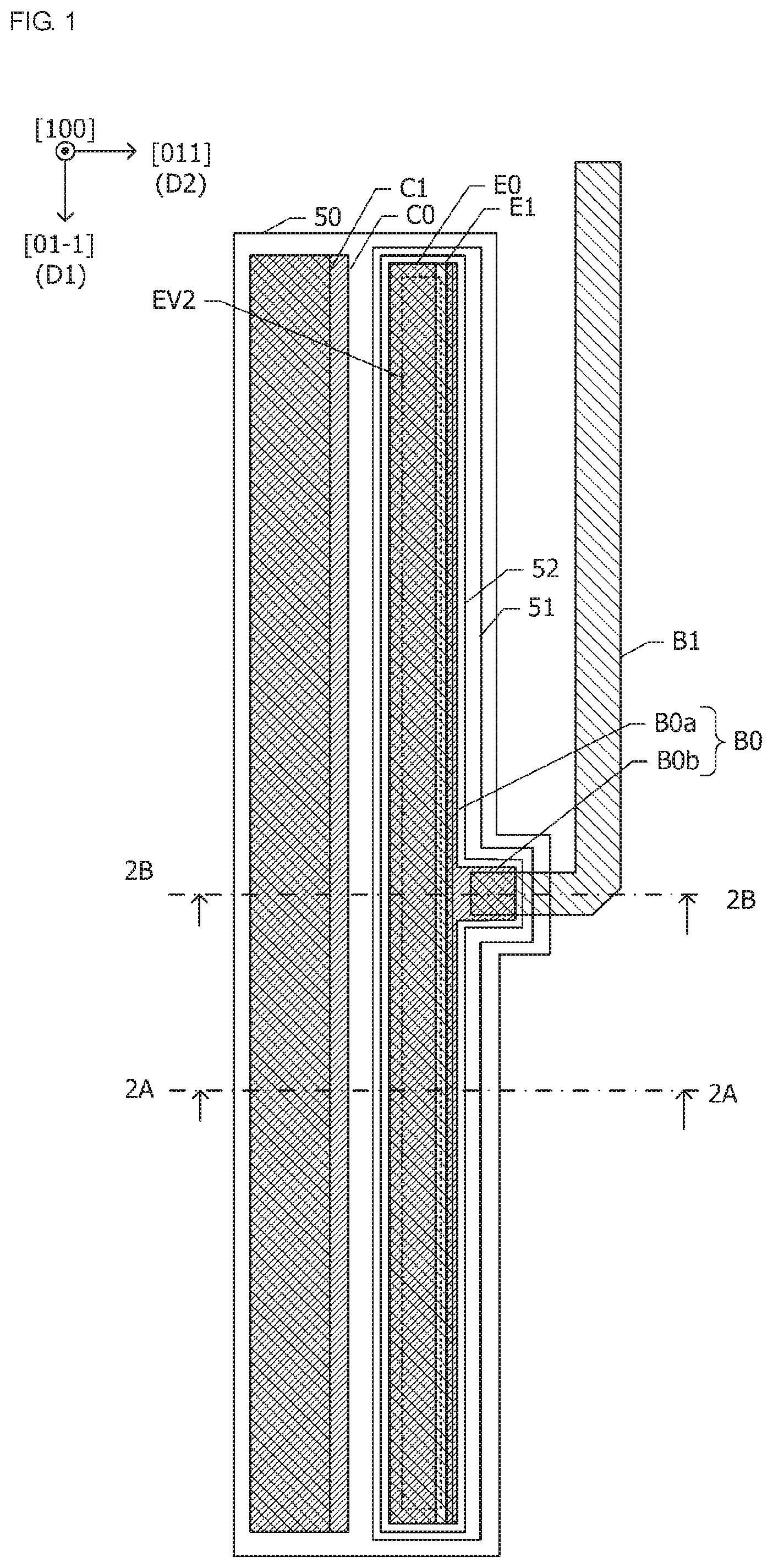
illustrates a planar layout of constituent elements of the semiconductor device according to the first example. A and 2 B are sectional views of the semiconductor device respectively taken along dash-dot line 2 A- 2 A and dash-dot line 2 B- 2 B in . A and 2 B are sectional views of the semiconductor device, illustrating constituent elements thereof with a focus on their positional relationship in the height direction. It should be noted that their positional relationship in the lateral direction does not fully correspond to the layout illustrated in .
The semiconductor device according to the first example includes a (100)GaAs substrate 70 . A sub-collector layer 50 , which is electrically conductive, is provided in a surface layer portion of the substrate 70 and is surrounded by an insulating region 71 . The sub-collector layer 50 is formed from, for example, n-type GaAs epitaxially grown on the substrate 70 . The insulating region 71 surrounding the sub-collector layer 50 is formed by implanting hydrogen ions (protons) into the n-type GaAs layer. A collector mesa 51 , which is mesa-shaped, and a collector electrode C 0 are located within the sub-collector layer 50 when viewed in plan.
When viewed in plan, the collector mesa 51 and the collector electrode C 0 are long in the [01-1] direction of the substrate and are discretely located away from each other in the [011] direction. The minus sign in a Miller index is equivalent to an overbar added to a Miller index. The longitudinal direction of the collector mesa 51 and the collector electrode C 0 is herein referred to as a first direction D 1 . A direction orthogonal to the first direction D 1 in a surface of the substrate is herein referred to as a second direction D 2 .
A base mesa 52 , which is mesa-shaped, is located within the collector mesa 51 when viewed in plan. The collector mesa 51 includes a collector layer CL, and the base mesa 52 includes a base layer BL, which is disposed on the collector layer CL. The collector mesa 51 is located within the sub-collector layer 50 and is closer to one side than to the other side of the sub-collector layer 50 in the second direction D 2 when viewed in plan.
An emitter electrode E 0 and a base electrode B 0 are located within the base mesa 52 when viewed in plan. The emitter electrode E 0 and the base electrode B 0 are long in the first direction D 1 when viewed in plan. The emitter electrode E 0 and the base electrode B 0 are discretely located away from each other in the second direction D 2 . An emitter layer EL is disposed between the emitter electrode E 0 and the base layer BL. The emitter layer EL mostly overlaps the emitter electrode E 0 when viewed in plan. The emitter layer EL is not explicitly illustrated in . The collector layer CL and the base layer BL are respectively formed from, for example, n-type GaAs and p-type GaAs. The emitter layer EL may include: an n-type InGaP layer; and an emitter cap layer and a contact layer that are disposed on or above the n-type InGaP layer. The emitter cap layer and the contact layer are respectively formed from, for example, n-type GaAs and n-type InGaAs, each of which is more highly concentrated than the constituent of the emitter layer EL. The collector layer CL, the base layer BL, and the emitter layer EL are arranged in the stated order from closest to the substrate 70 in the thickness direction of the substrate 70 to constitute a heterojunction bipolar transistor (HBT).
The base electrode B 0 includes a main portion B 0 a and a connecting portion B 0 b (see ). The main portion B 0 a extends in the first direction D 1 and has a fixed width. The connecting portion B 0 b protrudes from a midsection of the main portion B 0 a toward one side in the second direction D 2 (the right side in ). The base mesa 52 , the collector mesa 51 , and the sub-collector layer 50 are designed to resemble the shape of the base electrode B 0 viewed in plan and include protruding portions corresponding to the connecting portion B 0 b of the base electrode B 0 .
The collector electrode C 0 is electrically connected to the collector layer CL via the sub-collector layer 50 . The base electrode B 0 is electrically connected to the base layer BL. The emitter electrode E 0 is electrically connected to the emitter layer EL. The collector electrode C 0 , the emitter electrode E 0 , and the base electrode B 0 are arranged in the stated order in the second direction D 2 . That is, the collector electrode C 0 is located on one side in the second direction D 2 with respect to the emitter electrode E 0 and is not located on the other side when viewed in plan.
The collector electrode C 0 , the emitter electrode E 0 , and the base electrode B 0 are covered with an insulating film (not illustrated). A first-layer collector line C 1 , a first-layer emitter line E 1 , and a first-layer base line B 1 are disposed on the insulating film. Referring to , the collector electrode C 0 , the emitter electrode E 0 , and the base electrode B 0 are densely hatched with lines slanting up from left to right, and the first-layer collector line C 1 , the first-layer emitter line E 1 , and the first-layer base line B 1 are less densely hatched with lines slanting down from left to right.
The first-layer collector line C 1 extends through a cavity CV 1 in the insulating film disposed thereunder and is electrically connected to the collector electrode C 0 accordingly. The first-layer emitter line E 1 extends through a cavity EV 1 in the insulating film disposed thereunder and is electrically connected to the emitter electrode E 0 accordingly. The first-layer base line B 1 extends through a cavity BV 1 in the insulating film disposed thereunder and is electrically connected to the connecting portion B 0 b of the base electrode B 0 accordingly. When viewed in plan, the first-layer base line B 1 overlapping the connecting portion B 0 b of the base electrode B 0 extends in the second direction D 2 beyond an edge of the sub-collector layer 50 and then bends at a right angle to extend in the first direction D 1 .
The first-layer collector line C 1 , the base line B 1 , and the emitter line E 1 are covered with a second-layer insulating film (not illustrated). A second-layer emitter line E 2 (see A and 2 B ) is disposed on the insulating film. The second-layer emitter line E 2 extends through a cavity EV 2 in the insulating film disposed thereunder and is electrically connected to the first-layer emitter line E 1 accordingly. In , the cavity EV 2 is denoted by a broken line. A protective film (not illustrated) is disposed on the second-layer emitter line E 2 and has a cavity EV 3 , which is provided for a bump. An emitter bump E 3 is disposed so as to be in contact with the second-layer emitter line E 2 in the cavity EV 3 . The emitter bump E 3 slightly extends beyond the edge of the cavity EV 3 when viewed in plan.
The following describes advantageous effects of the first example with reference to to 6 .
illustrates a layout of constituent elements of the semiconductor device according to the first example and a layout of constituent elements of a semiconductor device according to a comparative example, with the semiconductor devices being viewed in plan. The semiconductor device according to the first example is illustrated on the left side of , and the semiconductor device according to the comparative example is illustrated on the right side of . As for the semiconductor device according to the first example, the connecting portion B 0 b is at the center of the base electrode B 0 in the first direction D 1 . That is, the first-layer base line B 1 is connected to the base electrode B 0 in a manner so as to adjoin the longitudinal center of the base electrode B 0 . As for the semiconductor device according to the comparative example, the connecting portion B 0 b is provided as an end portion (at an upper end in ) of the base electrode B 0 . That is, the first-layer base line B 1 is connected to a longitudinal end portion of the base electrode B 0 .
The second-layer emitter line E 2 is disposed in such a manner that the emitter electrode E 0 is located within the second-layer emitter line E 2 when viewed in plan. The emitter bump E 3 is also located within the second-layer emitter line E 2 when viewed in plan. The emitter bump E 3 extends through the cavity EV 3 and is connected to the second-layer emitter line E 2 accordingly. The emitter electrode E 0 , the first-layer emitter line E 1 , the second-layer emitter line E 2 , the cavity EV 3 , and the emitter bump E 3 are substantially symmetric with respect to the first direction D 1 .
When the transistor is active, operating current i 0 (see A and 2 B ) flows from the collector electrode C 0 and passes through the sub-collector layer 50 , the collector layer CL, the base layer BL, and the emitter layer EL. The operating current i 0 then enters the emitter electrode E 0 . The operating current generates heat while flowing in the thickness direction through the emitter layer EL, the base layer BL, and the collector layer CL (see A and 2 B ), which are located immediately below the emitter electrode E 0 . The heat is then transferred to the outside through the emitter electrode E 0 , the first-layer emitter line E 1 , the second-layer emitter line E 2 , and the emitter bump E 3 .
The operating current flowing through a joint interface between the base and the emitter is relatively great in magnitude at a point where the base resistance is relatively low. The base resistance is lower in the connecting portion B 0 b than in any other portion of the base electrode B 0 . A region farther from the connecting portion B 0 b in the first direction D 1 has a higher base resistance. As for the semiconductor device according to the first example, the magnitude of the operating current is greater in the longitudinal center of the emitter electrode E 0 than in any other region, and the same holds for the amount of heat generated. Referring to , regions in which a greater amount of heat is generated are more densely hatched. As for the semiconductor device according to the comparative example, the magnitude of the operating current is greater in a region including the upper end of the emitter electrode E 0 than in any other region, and the same holds for the amount of heat generated.
With a heat transfer path extending from a heat generation region to an upper surface of the emitter bump E 3 , the thermal resistance is lower in a region including a midsection of the emitter bump E 3 than in any other region in the first direction D 1 and is higher in regions closer to ends of the emitter bump E 3 . In the first example, the thermal resistance is relatively low in a region in which the amount of heat generated is greater than the amount of heat generated in another region in the first direction D 1 . The temperature distribution in the first direction D 1 is leveled accordingly. In the comparative example, meanwhile, the thermal resistance in a region including the upper end in which the amount of heat generated is greater than the amount of heat generated in any other region in the first direction D 1 is higher than the thermal resistance in the region including the midsection. The temperature distribution thus tends to be uneven.
A illustrates a layout of constituent elements of a semiconductor device according to another comparative example, with the semiconductor device being viewed in plan. B is a sectional view of the semiconductor device taken along dash-dot line 4 B- 4 B in A . In this comparative example, two base electrodes B 0 are disposed on opposite sides in the second direction with respect to the emitter electrode E 0 . The base electrodes B 0 disposed on the opposite sides with respect to the emitter electrode E 0 are connected to each other in an end portion via the connecting portion B 0 b . The connecting portion B 0 b is connected with the first-layer base line B 1 . Two collector electrodes C 0 are disposed on opposite sides in the second direction D 2 with respect to the collector mesa 51 .
The collector electrodes C 0 are connected with corresponding first-layer collector lines C 1 , and the emitter electrode E 0 is connected with the first-layer emitter line E 1 . The first-layer emitter line E 1 is connected with the second-layer emitter line E 2 , and the emitter bump E 3 is disposed on the second-layer emitter line E 2 .
When the transistor is active, operating current i 1 , which is denoted by arrows in B , flows from the collector electrode C 0 on the left side and from the collector electrode C 0 on the right side and passes through the sub-collector layer 50 , the collector layer CL, the base layer BL, and the emitter layer EL. The operating current i 1 then reaches a left end and a right end of the emitter electrode E 0 . Operating current i 2 flows from the collector electrode C 0 on the left side toward the right end of the emitter electrode E 0 , and operating current i 3 flows from the collector electrode C 0 on the right side toward the left end of the emitter electrode E 0 . The operating current i 2 and the operating current i 3 cancel each other if they have precise left-right symmetry in terms of electrical characteristics and thermal characteristics. If there is an imbalance between the right side and the left side, the operating current i 2 and the operating current i 3 do not cancel each other. In the heat generation region immediately below the emitter electrode E 0 , the amount of heat generated on the right side becomes out of proportion with the amount of heat generated on the left side.
A illustrates a layout of constituent elements of a semiconductor device according to still another comparative example, with the semiconductor device being viewed in plan. B is a sectional view of the semiconductor device taken along dash-dot line 5 B- 5 B in A . In this comparative example, two emitter electrodes E 0 are discretely located away from each other in the second direction D 2 . The base electrode B 0 is disposed between the two emitter electrodes E 0 . Two collector electrodes C 0 are disposed on opposite sides in the second direction D 2 with respect to the collector mesa 51 .
When the transistor is active, the operating current i 1 , which is denoted by arrows in B , flows from the collector electrode C 0 on the left side and from the collector electrode C 0 on the right side and passes through the sub-collector layer 50 , the collector layer CL, the base layer BL, and the emitter layer EL. The operating current i 1 then reaches the emitter electrode E 0 on the right side and the emitter electrode E 0 on the left side. The operating current i 2 flows from the collector electrode C 0 on the left side toward the emitter electrode E 0 on the right side, and the operating current i 3 flows from the collector electrode C 0 on the right side toward the emitter electrode E 0 on the left side. The operating current i 2 and the operating current i 3 cancel each other if they have precise left-right symmetry in terms of electrical characteristics and thermal characteristics. If there is an imbalance between the right side and the left side, the operating current i 2 and the operating current i 3 do not cancel each other. The amount of heat generated in the heat generation region immediately below the emitter electrode E 0 on the right side becomes out of proportion with the amount of heat generated in the heat generation region immediately below the emitter electrode E 0 on the left side.
The imbalance between the amount of heat generated on the right side and the amount of heat generated on the left side in the transistors according to the comparative examples illustrated in A to 5 B causes higher concentrations of operating current in higher-temperature regions. Consequently, an increase in power consumption will eventually lead to a breakdown in some cases. Such an imbalance in the amount of heat generated is created by the operating current flowing both rightward and leftward in the second direction D 2 .
Unlike the semiconductor devices according to these comparative examples, the semiconductor device according to the first example (see A and 2 B ) is configured in such a manner that the operating current i 0 flowing from the collector electrode C 0 toward the emitter electrode E 0 is directed from only one side to the other side in the second direction D 2 (from left to right in A and 2 B ). This eliminates the need to balance the operating current flowing rightward in the second direction D 2 and the operating current flowing leftward in the second direction D 2 . Thus, there is no cause for concern about such an imbalance in the amount of heat generated. Consequently, this configuration produces the effect of eliminating or reducing the possibility that the breakdown withstand voltage will be lowered due to concentration of generated heat in a particular spot.
The semiconductor device (a sample S 0 ) according to the first example, the semiconductor device (a sample S 4 ) according to the comparative example illustrated in A and 4 B , and the semiconductor device (a sample S 5 ) according to the comparative example illustrated in A and 5 B were prepared. These samples were subjected to measurements of transition voltage at the SOA boundary and voltage at the breakdown boundary. The SOA herein refers to a collector voltage range and a collector current range in which a transistor can operate in a stable manner without self-damage. The transition voltage is defined as a collector voltage at which an SOA line, namely, an SOA boundary obtained by increasing the collector voltage, plummets in a graph that represents the relationship between the collector voltage and the collector current. The breakdown boundary herein refers to a boundary between a collector voltage range and a collector current range in which a breakdown (a short circuit or breaking of electrical contact) in a transistor is avoided.
is a graph obtained by measurements conducted on the samples S 0 , S 4 , and S 5 , illustrating the relationship between transition voltage at the SOA boundary and voltage at the breakdown boundary. The horizontal axis represents the transition voltage at the SOA boundary in units of V, and the vertical axis represents the voltage at the breakdown boundary in units of V. The results show that the transition voltage at the SOA boundary and the voltage at the breakdown boundary are higher in the semiconductor device (the sample S 0 ) according to the first example than in each of the semiconductor device (the sample S 4 ) according to the comparative example illustrated in A and 4 B and the semiconductor device (the sample S 5 ) according to the comparative example illustrated in A and 5 B . The semiconductor device according to the first example produces the advantageous effect of enlarging the SOA and increasing the breakdown withstand voltage to a greater extent than would be possible with the semiconductor devices according to the comparative examples illustrated in A to 5 B .
The following describes a semiconductor device according to a modification of the first example with reference to .
is a sectional view of the semiconductor device according to the present modification of the first example. As for the semiconductor device according to the first example (see A and 2 B ), the insulating region 71 formed by proton implantation defines the periphery of the sub-collector layer 50 . In the modification illustrated in , both the n-type GaAs layer that is to be formed into the sub-collector layer 50 and the surface layer portion of the substrate 70 are etched to define the periphery of the sub-collector layer 50 . An insulating film is disposed in a recessed portion 72 , which is formed by the etching. The insulating film fitting in the recessed portion 72 formed by the etching serves as an insulating region, which surrounds the sub-collector layer 50 when viewed in plan.
The following describes a semiconductor device according to another modification of the first example with reference to .
is a sectional view of the semiconductor device according to the present modification of the first example. As for semiconductor device according to the first example (see A and 2 B ), the collector mesa 51 formed by etching an n-type GaAs layer that is to be formed into the collector layer CL and by eliminating an unnecessary portion from the n-type GaAs layer defines the periphery of the collector layer CL. In the modification illustrated in , protons are implanted into an unnecessary portion of an n-type GaAs layer that is to be formed into the collector layer CL, and the unnecessary portion is thus formed into an insulating region 73 , which defines part of the periphery of the collector layer CL. The insulating region 73 also defines the periphery of the sub-collector layer 50 .
The n-type GaAs that is to be formed into the collector layer CL is etched to form a recessed portion 74 in a region in which the collector electrode C 0 is to be disposed. The recessed portion 74 extends to the sub-collector layer 50 . The collector electrode C 0 is disposed so as to be in contact with the sub-collector layer 50 in the recessed portion 74 . Part of the periphery of the collector layer CL is defined by the recessed portion 74 . In the present modification, the collector layer CL whose periphery is defined by the insulating region 73 and the recessed portion 74 corresponds to the collector mesa 51 (see , 2 A, and 2 B ) in the first example.
The following describes other modifications of the first example.
It is not required that the connecting portion B 0 b of the base electrode B 0 adjoin the midsection of the main portion B 0 a in the first direction D 1 as in the first example (see ). The connecting portion B 0 b may adjoin any portion other than end portions of the main portion B 0 a . That is, the base line B 1 may be connected to the base electrode B 0 in a manner so as to adjoin a portion other than the longitudinal ends of the base electrode B 0 . The temperature distribution in the heat generation region may be leveled to a greater extent than would be possible with the layout in the comparative example in , in which the connecting portion B 0 b adjoins the end portion of the main portion B 0 a . To ensure adequate leveling of temperature distribution, the connecting portion B 0 b is preferably disposed in such a manner that the distance in the first direction D 1 between the center of the base electrode B 0 in the first direction D 1 and the connecting portion B 0 b (the point of connection between the base electrode B 0 and the base line B 1 ) is less than or equal to ¼ times the length of the base electrode B 0 .
In the first example, the collector layer CL is formed from n-type GaAs, the base layer BL is formed from p-type GaAs, and the emitter layer EL is formed mainly from n-type InGaP. Alternatively, other compound semiconductors may be used. The structure of the semiconductor device according to the first example is applicable not only to heterojunction bipolar transistors but also to other commonly-used bipolar transistors. Although one heterojunction bipolar transistor illustrated in , 2 A, and 2 B is included in the semiconductor device described as the first example, more than one heterojunction bipolar transistor may be disposed on a substrate and may be connected in parallel to constitute an output-stage amplifier circuit. The heterojunction bipolar transistors are preferably arranged side by side in the second direction D 2 .
When viewed in plan (see ), the base mesa 52 in the first example is smaller than the collector mesa 51 and is located within the collector mesa 51 . As illustrated in the sectional views ( A and 2 B ), a step is formed along an edge of the base mesa 52 . Alternatively, the base mesa 52 and the collector mesa 51 may fit exactly on top of each other when viewed in plan. In this case, the base layer BL and the collector layer CL are etched all at once for patterning. Consequently, each side face of the base layer BL and a corresponding side face of the collector layer CL extend in a continuous manner.
Second Example
The following describes a semiconductor device according to a second example with reference to . Configurations common to the semiconductor device according to the first example (see , 2 A, and 2 B ) and the semiconductor device according to the second example will not be further elaborated here.
illustrates a planar layout of constituent elements of the semiconductor device according to the second example. is a sectional view of the semiconductor device taken along dash-dot line 10 - 10 in .
The first-layer emitter line E 1 in the first example (see ) is located within the base mesa 52 when viewed in plan. Meanwhile, the first-layer emitter line E 1 in the second example extends from the position of the emitter electrode E 0 to the side opposite to the side on which the collector electrode C 0 is disposed. The first-layer emitter line E 1 extends above the main portion B 0 a of the base electrode B 0 and extends in the second direction D 2 beyond the edge of the base mesa 52 and the edge of the collector mesa 51 . The cavity EV 2 for forming a connection between the first-layer emitter line E 1 and the second-layer emitter line E 2 also extends beyond the edge of the collector mesa 51 when viewed in plan. In the position of the connecting portion B 0 b of the base electrode B 0 , the first-layer emitter line E 1 does not extend in the second direction D 2 beyond the edge of the base mesa 52 and is located within the base mesa 52 so as not to interfere with the base line B 1 .
The following describes advantageous effects of the second example. As with the first example, the second example produces the advantageous effect of enlarging the SOA and increasing the breakdown withstand voltage. The cavity EV 2 is provided to form a connection between the first-layer emitter line E 1 and the second-layer emitter line E 2 . When viewed in plan, the cavity EV 2 in the second example has an area greater than the area of the cavity EV 2 in the first example. This configuration increases the cross-sectional area of the heat transfer path extending from the heat generation region of the bipolar transistor to the emitter bump E 3 and reduces the thermal resistance in the heat transfer path accordingly. Consequently, the efficiency of heat transfer from the heat generation region may be enhanced.
The following describes a modification of second example with reference to .
is a sectional view of a semiconductor device according to the present modification of the second example. In the present modification, protons are implanted into an unnecessary portion of an n-type GaAs that is to be formed into the collector layer CL and the unnecessary portion is thus formed into the insulating region 73 as in the case with illustrating one of the modifications of the first example. The first-layer emitter line E 1 extends beyond the edge of the base mesa 52 and is located within the collector layer CL when viewed in plan. In the present modification, advantageous effects similar to those of second example may be attained. Alternatively, the insulating region 73 may be extended. With the insulating region 73 being closer to the base mesa 52 , the first-layer emitter line E 1 extends beyond the edge of the collector layer CL when viewed in plan.
Third Example
The following describes a semiconductor device according to a third example with reference to . Configurations common to the semiconductor device according to the first example (see , 2 A, and 2 B ) and the semiconductor device according to the third example will not be further elaborated here.
illustrates a planar layout of constituent elements of the semiconductor device according to the third example. is a sectional view of the semiconductor device taken along dash-dot line 13 - 13 in .
The emitter electrode E 0 in the first example (see ) extends continuously from one end to the other end of base mesa 52 in the first direction D 1 . The emitter electrode E 0 in the third example is divided, at about the center of the base mesa 52 in the first direction D 1 , into two sections. The connecting portion B 0 b of the base electrode B 0 in the first example (see ) protrudes from the main portion B 0 a toward the side opposite to the side on which the collector electrode C 0 is disposed. The connecting portion B 0 b of the base electrode B 0 in the third example protrudes from the main portion B 0 a toward the collector electrode C 0 . The connecting portion B 0 b is disposed between the two sections into which the emitter electrode E 0 is divided. The connecting portion B 0 b is connected with the first-layer base line B 1 .
With the emitter electrode E 0 being divided into two sections, the first-layer emitter line E 1 is divided into two sections correspondingly. The two sections of the first-layer emitter line E 1 are connected to each other via the second-layer emitter line E 2 (see ).
The following describes advantageous effects of the third example. As with the first example, the third example, in which the emitter electrode E 0 is divided into two sections, produces the advantageous effect of enlarging the SOA and increasing the breakdown withstand voltage.
Fourth Example
The following describes a semiconductor device according to a fourth example with reference to . Configurations common to the semiconductor device according to the third example (see ) and the semiconductor device according to the fourth example will not be further elaborated here.
illustrates a planar layout of constituent elements of the semiconductor device according to the fourth example. The two sections into which the first-layer emitter line E 1 in the third example (see ) is divided are located within the base mesa 52 when viewed in plan. Meanwhile, as with the first-layer emitter line E 1 in the second example (see ), two sections of the first-layer emitter line E 1 in the fourth example extend from the position of the emitter electrode E 0 to the side opposite to the side on which the collector electrode C 0 is disposed. The two sections of the first-layer emitter line E 1 extend above the main portion B 0 a of the base electrode B 0 and extend in the second direction D 2 beyond the edge of the base mesa 52 and the edge of the collector mesa 51 . In the fourth example, the cavity EV 2 for forming a connection between first-layer emitter line E 1 and the second-layer emitter line E 2 also extends beyond the edge of the collector mesa 51 when viewed in plan.
The following describes advantageous effects of the fourth example. As with the third example, the fourth example produces the advantageous effect of enlarging the SOA and increasing the breakdown withstand voltage. Furthermore, the efficiency of heat transfer from the heat generation region may be enhanced as in the second example.
Fifth Example
The following describes a semiconductor device according to a fifth example with reference to . Configurations common to the semiconductor device according to the third example (see ) and the semiconductor device according to the fifth example will not be further elaborated here.
illustrates a planar layout of constituent elements of the semiconductor device according to the fifth example. is a sectional view of the semiconductor device taken along dash-dot line 16 - 16 in . The base electrode B 0 in the third example (see ) is disposed so as to be opposite to the collector electrode C 0 in the second direction D 2 with the emitter electrode E 0 therebetween. Meanwhile, the main portion B 0 a of the base electrode B 0 in the fifth example is disposed between the emitter electrode E 0 and the collector electrode C 0 in the second direction D 2 .
The connecting portion B 0 b of the base electrode B 0 adjoins the midsection of the main portion B 0 a of the base electrode B 0 in the first direction D 1 . The connecting portion B 0 b protrudes from the main portion B 0 a toward the side opposite to the side on which the collector electrode C 0 is disposed. The emitter electrode E 0 is divided, at the position of the connecting portion B 0 b of the base electrode B 0 , into two sections. Similarly, the first-layer emitter line E 1 is divided into two sections. One end of the first-layer base line B 1 is disposed between the two sections of the first-layer emitter line E 1 and is connected to the connecting portion B 0 b of the base electrode B 0 accordingly.
The following describes advantageous effects of the fifth example. As with the collector electrode C 0 in the first example, the collector electrode C 0 in the fifth example is located on one side in the second direction D 2 with respect to the emitter electrode E 0 and is not located on the other side. Consequently, the operating current i 0 flowing from the collector electrode C 0 toward the emitter electrode E 0 is directed from only one side to the other side in the second direction D 2 . As with the first example, the fifth example thus produces the advantageous effect of enlarging the SOA and increasing the breakdown withstand voltage.
The first example (see ) necessitates, in the second direction D 2 , the space for the connecting portion B 0 b of the base electrode B 0 in addition to the space for the collector electrode C 0 , the emitter electrode E 0 , and the main portion B 0 a of the base electrode B 0 . In the fifth example, meanwhile, the connecting portion B 0 b of the base electrode B 0 and the emitter electrode E 0 are in the same position in the second direction D 2 . This layout enables a reduction in the dimension of the bipolar transistor in the second direction D 2 .
Sixth Example
The following describes a semiconductor device according to a sixth example with reference to . Configurations common to the semiconductor device according to the fifth example (see ) and the semiconductor device according to the sixth example will not be further elaborated here.
illustrates a planar layout of constituent elements of the semiconductor device according to the sixth example. The first-layer emitter line E 1 in the fifth example (see ) is located within the base mesa 52 when viewed in plan. Meanwhile, as with the first-layer emitter line E 1 in the fourth example (see ), the first-layer emitter line E 1 in the sixth example extends beyond the edge of the collector mesa 51 when viewed in plan. With the first-layer emitter line E 1 extending beyond the edge of the collector mesa 51 , the cavity EV 2 extends beyond the edge of the collector mesa 51 correspondingly.
The following describes advantageous effects of the sixth example.
As with the fifth example, the sixth example produces the advantageous effect of enlarging the SOA and increasing the breakdown withstand voltage. Furthermore, the efficiency of heat transfer from the heat generation region may be enhanced as in the fourth example.
Seventh Example
The following describes a semiconductor device according to a seventh example with reference to . Configurations common to the semiconductor device according to the third example (see ) and the semiconductor device according to the seventh example will not be further elaborated here.
illustrates a planar layout of constituent elements of the semiconductor device according to the seventh example. is a sectional view of the semiconductor device taken along dash-dot line 19 - 19 in .
The main portion B 0 a of the base electrode B 0 in the third example (see ) is disposed on only one side in the second direction D 2 with respect to the emitter electrode E 0 . In the seventh example, meanwhile, two main portions B 0 a of the base electrode B 0 are disposed on opposite sides with respect to the emitter electrode E 0 . The connecting portion B 0 b of the base electrode B 0 is disposed between two sections into which the emitter electrode E 0 is divided. The connecting portion B 0 b forms a connection between the two main portions B 0 a . The base electrode B 0 is thus H-shaped when viewed in plan.
The following describes advantageous effects of the seventh example.
In the seventh example, the main portions B 0 a of the base electrode B 0 are disposed on opposite sides in the second direction with respect to the emitter electrode E 0 , whereas the collector electrode C 0 is disposed on only one side as in the third example (see ). Consequently, the operating current i 0 (see ) flowing from the collector electrode C 0 toward the emitter electrode E 0 is directed from only one side to the other side in the second direction D 2 . As with the third example, the seventh example produces the advantageous effect of enlarging the SOA and increasing the breakdown withstand voltage.
Furthermore, the main portions B 0 a of the base electrode B 0 in the seventh example are disposed on the opposite sides with respect to the emitter electrode E 0 , and the base resistance is thus reduced to a greater extent than would be possible with the layout in the third example.
Eighth Example
The following describes a semiconductor device according to an eighth example with reference to . Configurations common to the semiconductor device according to the seventh example (see ) and the semiconductor device according to the eighth example will not be further elaborated here.
illustrates a planar layout of constituent elements of the semiconductor device according to the eighth example. The first-layer emitter line E 1 in the seventh example (see ) is located within the base mesa 52 when viewed in plan. Meanwhile, as with the first-layer emitter line E 1 in the fourth example (see ), the first-layer emitter line E 1 in the eighth example extends beyond the edge of the base mesa 52 and the edge of the collector mesa 51 when viewed in plan.
The following describes advantageous effects of the eighth example.
As with the seventh example, the eighth example produces the advantageous effect of enlarging the SOA and increasing the breakdown withstand voltage. Furthermore, the efficiency of heat transfer from the heat generation region may be enhanced in the eighth example as in the fourth example.
Ninth Example
The following describes a semiconductor device according to a ninth example with reference to . Configurations common to the semiconductor device according to the first example and the semiconductor device according to the ninth example will not be further elaborated here.
illustrates a planar layout of constituent elements of the semiconductor device according to the ninth example. The collector electrode C 0 , the emitter electrode E 0 , the base electrode B 0 , the first-layer collector line C 1 , the first-layer emitter line E 1 , and the first-layer base line B 1 have shapes and relative positional relationship identical to the shape and the relative positional relationship of the corresponding constituent elements in the first example (see ) when viewed in plan. The difference between the first and ninth examples is in the first direction D 1 , namely, the longitudinal direction of the emitter electrode E 0 . Specifically, the first direction D 1 in the first example (see ) coincides with the [01-1] direction of the substrate 70 formed from single-crystal GaAs, whereas the first direction D 1 in the ninth example coincides with the [011] direction of the substrate 70 .
In the first example (see ), a portion being part of the first-layer base line B 1 and extending out from the connecting portion B 0 b in the second direction D 2 intersects the edge of the collector mesa 51 parallel to the first direction D 1 . In the ninth example, meanwhile, the portion extending out from the connecting portion B 0 b in the second direction D 2 is located within the collector mesa 51 when viewed in plan. The portion being part of the base line B 1 and located within the collector mesa 51 is bent at a right angle, and the remaining portion of the base line B 1 extends in the first direction D 1 . The portion being part of the base line B 1 and extending in the first direction D 1 intersects the edge of the collector mesa 51 parallel to the second direction D 2 . That is, both the first-layer base line B 1 in the first example (see ) and the first-layer base line B 1 in the ninth example intersect the edge of the collector mesa 51 parallel to the [01-1] direction when viewed in plan.
The following describes advantageous effects of the ninth example. As with the first example, the ninth example produces the advantageous effect of enlarging the SOA and increasing the breakdown withstand voltage.
Side faces of the collector mesa 51 formed by wet etching of the GaAs layer that is to be formed into the collector layer CL (see A ) are inclined and are not perpendicular to an upper surface of the substrate 70 due to the anisotropy of etching speed. The side faces of the collector mesa 51 viewed in section as in A , that is, the side faces extending in the [01-1] direction are inclined at an angle of less than 90°. The shape defined with side faces inclined at angle of less than 90° is herein referred to as a normal mesa shape. The other side faces of collector mesa 51 extend in the [011] direction and are inclined at an angle of greater than 90°. The shape defined with side faces inclined at an angle of greater than 90° is referred to as an inverted mesa shape.
The first-layer base line B 1 disposed in a manner so as to intersect one of side faces defining an inverted mesa shape is liable to break. To avoid breakage, the first-layer base line B 1 is preferably disposed in a manner so as to intersect one of side faces of the collector mesa 51 that define a normal mesa shape. In the first example (see B ), the first-layer base line B 1 intersects one of the side faces of the collector mesa 51 that extend in the [01-1] direction and define a normal mesa shape. In the ninth example (see ), the portion being part of the first-layer base line B 1 and located within the collector mesa 51 when viewed in plan is bent at a right angle. The first-layer base line B 1 thus intersects one of the side faces of the collector mesa 51 that extend in the [01-1] direction and define a normal mesa shape. The ninth example thus eliminates or reduces the occurrence of breakage of the first-layer base line B 1 .
When viewed in plan, the first-layer base line B 1 intersects one of side faces of the base mesa 52 that define an inverted mesa shape. The height of the side face of the base mesa 52 is sufficiently smaller than the height of the corresponding side face of the collector mesa 51 . Thus, the first-layer base line B 1 intersecting one of the side faces of the base mesa 52 that define an inverted mesa shape is not liable to break.
The following describes semiconductor devices according to modifications of the ninth example with reference to to 28 . In the modifications respectively illustrated in to 28 , the first direction D 1 , namely the longitudinal direction of the emitter electrode E 0 coincides with the [011] direction of the substrate 70 as in the ninth example (see ). As with the first-layer base line B 1 in the ninth example, the first-layer base line B 1 in each of the modifications intersects one of the side faces of the collector mesa 51 that extend in the second direction D 2 ([01-1] direction).
The collector electrode C 0 , the emitter electrode E 0 , the base electrode B 0 , the first-layer collector line C 1 , the first-layer emitter line E 1 , and the first-layer base line B 1 in the modification illustrated in have shapes and positional relationship identical to the shapes and the positional relationship of the corresponding constituent elements in the second example (see ) when viewed in plan. The constituent elements in the modification illustrated in have shapes and positional relationship identical to the shapes and the positional relationship of the corresponding constituent elements in the third example (see ) when viewed in plan. The constituent elements in the modification illustrated in have shapes and positional relationship identical to the shapes and the positional relationship of the corresponding constituent elements in the fourth example (see ) when viewed in plan. The constituent elements in the modification illustrated in have shapes and positional relationship identical to the shapes and the positional relationship of the corresponding constituent elements in the fifth example (see ) when viewed in plan. The constituent elements in the modification illustrated in have shapes and positional relationship identical to the shapes and the positional relationship of the corresponding constituent elements in the sixth example (see ) when viewed in plan. The constituent elements in the modification illustrated in have shapes and positional relationship identical to the shapes and the positional relationship of the corresponding constituent elements in the seventh example (see ) when viewed in plan. The constituent elements in the modification illustrated in have shapes and positional relationship identical to the shapes and the positional relationship of the corresponding constituent elements in the eighth example (see ) when viewed in plan.
As with the ninth example, these modifications produce the advantageous effect of enlarging the SOA and increasing the higher breakdown withstand voltage and the effect of eliminating or reducing the occurrence of breakage of the first-layer base line B 1 . Furthermore, these modifications also produce effects similar to those of the corresponding ones of the second to eighth examples.
Tenth Example
The following describes a semiconductor device according to a tenth example with reference to . Configurations common to the semiconductor device according to the second example (see ) and the semiconductor device according to the tenth example will not be further elaborated here.
illustrates a planar layout of constituent elements of the semiconductor device according to the tenth example. In the second example (see ), the base electrode B 0 includes one connecting portion B 0 b , and the first-layer base line B 1 and the base electrode B 0 are connected to each other in one position. In the tenth example, meanwhile, the base electrode B 0 includes two connecting portions B 0 b , and the first-layer base line B 1 and the base electrode B 0 are connected to each other in two different positions in the first direction D 1 . The two connecting portions B 0 b are in positions other than the both ends of the base electrode B 0 and are located at equal distances from the center of the base electrode B 0 in the first direction D 1 .
The following describes advantageous effects of the tenth example.
In the tenth example, the base resistance distribution in the first direction D 1 is leveled to a greater extent than would be possible in the first example. Consequently, the base current distribution in the first direction D 1 is also leveled, and the distribution of the amount of heat generated in the heat generation region of the bipolar transistor is leveled accordingly.
illustrates a layout of the constituent elements of the semiconductor device according to the first example and a layout of the constituent elements of the semiconductor device according to the tenth example, with the semiconductor devices being viewed in plan. The semiconductor device according to the first example is illustrated on the left side of , and the semiconductor device according to the tenth example is illustrated on the right side of . The relative positional relationship in the first direction D 1 between the emitter electrode E 0 , the first-layer emitter line E 1 , the second-layer emitter line E 2 , the emitter bump E 3 , and the cavity EV 3 is as described above with reference to . Referring to , regions in which a greater amount of heat is generated are more densely hatched.
In both the first example and the tenth example, the amount of heat generated is greater in the position of the connecting portion B 0 b of the base electrode B 0 is greater than the amount of heat generated in any other region in the first direction D 1 . It should be noted that the degree of concentration of the amount of heat generated is lower in the tenth example than in the first example.
The thermal resistance in the heat transfer path extending from the heat generation region to the upper surface of the emitter bump E 3 varies in the first direction D 1 . The configuration in the first example or the configuration in the tenth example, whichever is better suited to the thermal resistance distribution concerned, may be adopted. For example, a decision on which configuration to adopt may be made in accordance with the difference in thermal resistance between each end and the center of the emitter electrode E 0 in the first direction D 1 .
The emitter layer EL and the emitter electrode E 0 are preferably extended in the first direction D 1 in view of, for example, the radio-frequency performance (e.g., the performance at 2.5 GHz) and the breakdown withstand voltage. In some cases, the length of each of the emitter layer EL and the emitter electrode E 0 in the first direction D 1 is greater than 100 μm. With the length of the emitter layer EL and the length of the emitter electrode E 0 being increased, the base electrode B 0 is extended in the first direction D 1 correspondingly. As the base electrode B 0 is extended, unevenness in the base electrode resistance in the first direction D 1 tends to increase. In this case, the base electrode B 0 and the base line B 1 are preferably connected to each other in more than one position as in the tenth example so that unevenness in base electrode resistance is reduced. In a case where the length of the base electrode B 0 in the first direction D 1 is less than or equal to 100 μm, the base electrode B 0 and the base line B 1 may be connected to each other in one position.
The two connecting portions B 0 b of the base electrode B 0 in the tenth example may be arranged in a manner so as to adjust the distribution of the amount of heat generated. For example, as the space between the two connecting portions B 0 b is reduced, the degree of concentration of the amount of heat generated increases. The positions of the connecting portions B 0 b in the first direction D 1 may be determined in accordance with the thermal resistance distribution. The temperature distribution in the heat generation region may be leveled to a greater extent accordingly.
The following describes modifications of the tenth example.
It is not required that the base electrode B 0 include two connecting portions B 0 b as in the tenth example. The base electrode B 0 may include three or more connecting portions B 0 b . The configuration with a larger number of connecting portions B 0 b offers a higher degree of flexibility in the control of distribution of the amount of heat generated.
It is not required that the two connecting portions B 0 b be located at equal distances from the center of the base electrode B 0 in the first direction D 1 as in the tenth example. When the thermal resistance distribution in the first direction D 1 is asymmetrical, the connecting portions B 0 b may be arranged asymmetrically in accordance with the thermal resistance distribution and may be located at different distances from the center of the base electrode B 0 .
Eleventh Example
The following describes a semiconductor device according to an eleventh example with reference to .
illustrates a layout of constituent elements of the semiconductor device according to the eleventh example, with the semiconductor device being viewed in plan. The first to tenth examples describe the configuration of the semiconductor devices each including one bipolar transistor. Meanwhile, the semiconductor device according to the eleventh example includes a plurality of bipolar transistors provided on a common substrate. Configuration of each bipolar transistor is similar to the configuration of the bipolar transistor included in the semiconductor device (see ) according to the second example. Together with each bipolar transistor, the collector electrode C 0 , the base electrode B 0 , and the emitter electrode E 0 that are connected the bipolar transistor (see ) are herein collectively referred to as a cell.
A plurality of cells 80 are arranged side by side in the second direction D 2 orthogonal to the longitudinal direction of the emitter electrode E 0 . The cells 80 are provided with their respective sub-collector layers 50 . Two sub-collector layers 50 adjacent to each other in the second direction D 2 are separated from each other by the insulating region 71 (see ).
The cells 80 are divided into a first group 81 and a second group 82 . The first group 81 and the second group 82 each include, for example, six cells 80 . The order in which the collector electrode C 0 , the emitter electrode E 0 , and the base electrode B 0 of one of the cells 80 in a group are arranged in the second direction D 2 and the order in which the corresponding electrodes of any other cell 80 in the group are arranged in the second direction D 2 are the same. The cells 80 belonging to the same group are spaced uniformly. The cells 80 belonging to the first group 81 and the cells 80 belonging to the second group 82 are arranged in mirror-image form in the second direction D 2 .
A second-layer emitter line E 2 overlaps the first-layer emitter lines E 1 of the cells 80 in the first group 81 when viewed in plan. Similarly, another second-layer emitter line E 2 overlaps the first-layer emitter lines E 1 of the cells 80 in the second group 82 when viewed in plan. Each of the second-layer emitter line E 2 is connected to the first-layer emitter lines E 1 of the cells 80 belonging to the corresponding one of the groups.
Emitter bumps E 3 are located within the two respective second-layer emitter lines E 2 when viewed in plan. The emitter bumps E 3 are long in the second direction D 2 when viewed in plan. The emitter bump E 3 extend through corresponding cavities EV 3 in the protective film disposed thereunder and are connected to the corresponding second-layer emitter lines E 2 accordingly. Each emitter bump E 3 overlaps the emitter electrodes E 0 of the cells 80 when viewed in plan. Each emitter electrode E 0 may partially extends beyond the edge of the emitter bump E 3 when viewed in plan.
First-layer collector lines C 1 extend out from the collector electrodes C 0 of the cells 80 in the first direction D 1 . The collector lines C 1 are linked to a first-layer collector common line C 1 c , which is long in the second direction D 2 . The collector common line C 1 c and the collector lines C 1 linked thereto form a comb shape when viewed in plan.
A second-layer collector line C 2 partially overlaps the collector common line C 1 c when viewed in plan. The second-layer collector line C 2 extends through a cavity CV 2 in an insulating film disposed thereunder and is connected to the first-layer collector common line C 1 c accordingly. A collector bump C 3 is located within the second-layer collector line C 2 and is located outside the first-layer collector common line C 1 c when viewed in plan. The collector bump C 3 is long in the second direction D 2 when viewed in plan. The longitudinal direction of the collector bump C 3 coincides with the longitudinal direction of the emitter bumps E 3 . Each emitter bump E 3 is larger than the collector bump C 3 when viewed in plan. The collector bump C 3 extends through a cavity CV 3 in a protective film disposed thereunder and is connected to the second-layer collector line C 2 accordingly.
First-layer base lines B 1 extend out from the base electrodes B 0 of the cells 80 in the first direction D 1 . The direction in which the base lines B 1 extend out from the corresponding electrodes is opposite to the direction in which the collector lines C 1 extend out from the corresponding electrodes. A radio-frequency signal input line RF 2 extends in the second direction D 2 and intersects the base lines B 1 when viewed in plan. The radio-frequency signal input line RF 2 is disposed in a second wiring layer. An overlap between each first-layer base line B 1 and the radio-frequency signal input line RF 2 functions as an input capacitive element 85 , with the base line B 1 and the radio-frequency signal input line RF 2 constituting a pair of electrodes. The portion being part of the base line B 1 and overlapping the radio-frequency signal input line RF 2 is wider than the other portion of the base line B 1 , and required capacitance is provided accordingly. The cells 80 are provided with their respective input capacitive elements 85 , which are arranged side by side in the second direction D 2 . The base lines B 1 extending out from the corresponding cells 80 intersect the radio-frequency signal input line RF 2 and are connected to a base common line B 1 c via corresponding ballast resistance elements 86 .
is an equivalent circuit diagram of the semiconductor device according to the eleventh example. The emitters of the bipolar transistors of the cells 80 belonging to the first group 81 are connected to one of the emitter bumps E 3 via one of the second-layer emitter lines E 2 . Similarly, emitters of the bipolar transistors of the cells 80 belonging to the second group 82 are connected to the other emitter bump E 3 via the other second-layer emitter line E 2 . The emitter bumps E 3 are connected to, for example, ground of a mounting substrate.
Collectors of the bipolar transistors of the cells 80 are connected to the collector bump C 3 via one collector common line C 1 c . Bases of the bipolar transistors of the cells 80 are connected to one radio-frequency signal input line RF 2 via the corresponding input capacitive elements 85 . Radio-frequency signals input through a radio-frequency signal input terminal RFin flow through the radio-frequency signal input line RF 2 and then enter the bases of the bipolar transistors of the cells 80 . The bases of the bipolar transistors of the cells 80 are also connected to the base common line B 1 c via the corresponding ballast resistance elements 86 . Base bias is provided from a base bias terminal BB to the bipolar transistors of the cells 80 , through the base common line B 1 c.
As illustrated in , the cells 80 in the eleventh example are connected in parallel to constitute a power amplifier circuit. The semiconductor device according to the eleventh example is mounted face-down on the mounting substrate by flip-chip mounting.
The following describes advantageous effects of the eleventh example.
Each of the cells 80 in the eleventh example is the semiconductor device according to the second example. As with the second example, the eleventh example enables enlargement of the SOA and an increase in breakdown withstand voltage. Each of the emitter bumps E 3 is larger than the collector bump C 3 . The eleventh example thus produces the advantageous effect of reducing the thermal resistance in the heat transfer paths of the bipolar transistors.
The following describes modifications of the eleventh example. Each of the cells 80 of the semiconductor device according to the eleventh example has a configuration identical to the configuration of the semiconductor device according to the second example. Alternatively, each of the cells 80 may have a configuration identical to the configuration of the semiconductor device according to any one of the first and third to tenth examples.
Twelfth Example
The following describes a semiconductor device according to a twelfth example with reference to . Configurations common to the semiconductor device according to the eleventh example (see ) and the semiconductor device according to the twelfth example will not be further elaborated here.
illustrates a layout of constituent elements of the semiconductor device according to the twelfth example, with the semiconductor device being viewed in plan. In the eleventh example (see ), the order in which the collector electrode C 0 , the emitter electrode E 0 , and the base electrode B 0 of one of the cells 80 in a group are arranged in the second direction D 2 and the order in which the corresponding electrodes of any other cell 80 in the group are the same. In the twelfth example, meanwhile, the collector electrode C 0 , the emitter electrode E 0 , and the base electrode B 0 of one of two adjacent ones of the cells 80 are arranged in the second direction D 2 in inverse order to those of the other cell. That is, the cells 80 adjacent to each other in the second direction D 2 are arranged in mirror-image form in the second direction D 2 . For example, the collector electrode C 0 , the emitter electrode E 0 , and the base electrode B 0 of each of the odd-numbered cells 80 counting from the left side of are arranged in the stated order in the direction from left to right, and the collector electrode C 0 , the emitter electrode E 0 , and the base electrode B 0 of each of the even-numbered cells 80 are arranged in the stated order in the direction from right to left.
The base electrode B 0 of each of the odd-numbered cells 80 counting from the left side and the base electrode B 0 of the cell 80 to the right are adjacent to each other. The collector electrode C 0 of each of the even-numbered cells 80 counting from the left side and the collector electrode C 0 of the cell 80 to the right are adjacent to each other. Two cells 80 whose collector electrodes C 0 are adjacent to each other in the second direction D 2 share the first-layer collector line C 1 connected to the two adjacent collector electrodes C 0 .
In the eleventh example (see ), two sub-collector layers 50 corresponding to two cells 80 adjacent to each other in the second direction D 2 are separated from each other by the insulating region 71 (see A and 2 B ). In the twelfth example, meanwhile, two cells 80 whose collector electrodes C 0 are adjacent to each other in the second direction D 2 are located within the sub-collector layer 50 common to the two cells 80 when viewed in plan. That is, two cells 80 whose collector electrodes C 0 are adjacent to each other in the second direction D 2 share one sub-collector layer 50 . The sub-collector layer 50 shared by two cells satisfies the following condition: on the sub-collector layer 50 , the collector electrode C 0 is disposed on only one side in the second direction D 2 with respect to the emitter electrode E 0 . Two sub-collector layers 50 corresponding to two cells 80 whose base electrodes B 0 are adjacent to each other in the second direction D 2 are separated from each other by insulating region 71 (see A and 2 B ).
The following describes advantageous effects of the twelfth example.
As with the eleventh example, the twelfth example enables enlargement of the SOA and an increase in breakdown withstand voltage. One of the features of the twelfth example is that two cells 80 whose collector electrodes C 0 are adjacent to each other in the second direction D 2 share one sub-collector layer 50 and one collector line C 1 . This feature enables a reduction in the dimension of the semiconductor device in the second direction D 2 .
In each of the cells 80 in the twelfth example, the emitter line E 1 is disposed between the first-layer base line B 1 and the first-layer collector line C 1 . The emitter line E 1 is connected to the ground. This configuration eliminates or reduces the possibility that the interference of radio-frequency signals will occur between the base line B 1 and the collector line C 1 .
The following describes a modification of the twelfth example. In the twelfth example, two cells 80 whose collector electrodes C 0 are adjacent to each other in the second direction D 2 share one sub-collector layer 50 and one collector line C 1 . In the present modification, the two cells 80 may also share one collector electrode C 0 .
Thirteenth Example
The following describes a semiconductor device according to a thirteenth example with reference to , 35 , and 36 . Configurations common to the semiconductor device according to the twelfth example (see ) and the semiconductor device according to the thirteenth example will not be further elaborated here.
illustrates a layout of constituent elements of the semiconductor device according to the thirteenth example, with the semiconductor device being viewed in plan. is a sectional view of the semiconductor device taken along dash-dot line 35 - 35 in . In the twelfth example ( ), the emitter bumps E 3 and the collector bump C 3 are used as terminals for external connection. In the semiconductor device according to the thirteenth example, meanwhile, a pad for wire bonding or the like is used as a terminal for external connection.
The following specifically describes the structure of the semiconductor device according to the thirteenth example. The second-layer emitter line E 2 is disposed in such a manner that the emitter electrodes E 0 of the cells 80 are located within the second-layer emitter line E 2 when viewed in plan. A first-layer ground line G 1 is disposed on one side in the first direction D 1 with respect to a row of the cells 80 . The first-layer ground line G 1 and the second-layer emitter line E 2 partially overlap each other when viewed in plan. In the overlapping regions, the first-layer ground line G 1 and the second-layer emitter line E 2 are connected to each other.
A second-layer collector common line C 2 c partially overlaps the first-layer ground line G 1 when viewed in plan. The second-layer collector common line C 2 c partially overlaps each of the first-layer collector lines C 1 when viewed in plan. In the overlapping regions, the second-layer collector common line C 2 c is connected to the collector lines C 1 .
A plurality of via holes 87 are located within the first-layer ground line G 1 when viewed in plan. The via holes 87 extend from the ground line G 1 to a back surface of the substrate 70 (see ). The ground line G 1 is exposed at bottom faces of the via hole 87 . A conductor film is formed on the back surface of the substrate 70 and on side faces and the bottom faces of the via holes 87 by means of the plating method. The conductor film includes: a ground conductor G 2 , which covers the back surface of the substrate 70 ; and conductor portions 88 , which cover the side faces and the bottom faces of the via holes 87 . The ground conductor G 2 is electrically connected to the ground line G 1 via the conductor portions 88 in the via holes 87 . The ground conductor G 2 on the back surface is soldered to a ground terminal of the mounting substrate, and the semiconductor device is fixed to the mounting substrate accordingly.
The second-layer collector common line C 2 c is covered with a protective film (not illustrated). The protective film has cavities, in which the collector common line C 2 c is exposed and is used as a collector terminal (collector pad) 89 for external connection.
is an equivalent circuit diagram of the semiconductor device according to the thirteenth example. Emitters of bipolar transistors of the cells 80 are connected to the ground line G 1 . The ground line G 1 is connected to the ground conductor G 2 on the back surface via the conductor portions 88 in the via holes 87 . The ground conductor G 2 is connected to the ground of the mounting substrate. Collectors of the bipolar transistors of the cells 80 are connected to the collector terminal 89 via the collector common line C 2 c . Connections associated with bases of the bipolar transistors of the cells 80 are as described in the eleventh example (see ).
The following describes advantageous effects of the thirteenth example. In the thirteenth example, the collector electrode C 0 is disposed on only one side in the second direction with respect to the emitter electrode E 0 , and the operating current is thus directed from only one side to the other side in the second direction, as in the twelfth example. The thirteenth example thus produces the advantageous effect of increasing the breakdown withstand voltage.
The following describes a modification of the thirteenth example. As with the cells 80 in the twelfth example, the cells 80 in the thirteenth example are arranged in such a manner that the adjacent cells 80 in the midsection of a row of cells are spaced further apart than the rest of the adjacent cells 80 are. Alternatively, the spacing between the adjacent cells 80 in the midsection may be equal to the spacing between the rest of the adjacent cells 80 .
Fourteenth Example
The following describes a semiconductor device according to a fourteenth example with reference to . Configurations common to the semiconductor device according to the twelfth example (see ) and the semiconductor device according to the twelfth example will not be further elaborated here.
illustrates a layout of constituent elements of the semiconductor device according to the fourteenth example, with the semiconductor device being viewed in plan. In the twelfth example (see ), two cells 80 whose base electrodes B 0 are adjacent to each other are provided with their respective first-layer base lines B 1 . In the fourteenth example, meanwhile, two adjacent ones of the cells 80 share part of one first-layer base line B 1 . More specifically, two cells 80 whose collector electrodes C 0 are located on outer sides with respect to their respective base electrodes B 0 share part of one base line B 1 .
The following describes a configuration of the first-layer base line B 1 . The base line B 1 includes portions extending out from two corresponding cells 80 whose collector electrodes C 0 are located on outer sides with respect to their respective base electrodes B 0 . The portions respectively extend toward one side and the other side in the second direction D 2 in a manner so as to come close to each other. The portions of the base line B 1 that extend out in the second direction D 2 are referred to as first portions. The first portions of the base line B 1 that respectively extend out from the two corresponding cells 80 are linked to each other. Another portion of the base line B 1 extends in the first direction D 1 from the midsection of the part composed of the first portions linked to each other. The portion extending in the first direction D 1 is herein referred to as a second portion. The second portion included in the base line B 1 and extending in the first direction D 1 is shared by the cells 80 located on opposite sides with respect to the base line B 1 .
With each of the base lines B 1 being shared by two cells 80 , each of the input capacitive elements 85 and each of the ballast resistance elements 86 are shared by two cells 80 correspondingly.
is an equivalent circuit diagram of the semiconductor device according to the fourteenth example. Bases of adjacent ones of the cells 80 are connected to each other, and two cells 80 are connected with one input capacitive element 85 and one ballast resistance element 86 .
The following describes advantageous effects of the fourteenth example. As with the twelfth example, the fourteenth example enables enlargement of the SOA and an increase in breakdown withstand voltage and eliminates or reduces the possibility that the interference of radio-frequency signals will occur between the base line B 1 and the collector line C 1 . One of the features of the fourteenth example is that two cells 80 share the second portion of one first-layer base line B 1 . This feature enables a reduction in the dimension of the semiconductor device in the second direction D 2 .
Fifteenth Example
The following describes a semiconductor device according to a fifteenth example with reference to . Configurations common to the semiconductor device according to the fourteenth example (see ) and the semiconductor device according to the fifteenth example will not be further elaborated here.
illustrates a layout of constituent elements of the semiconductor device according to the fifteenth example, with the semiconductor device being viewed in plan. In the fourteenth example (see ), one of the second-layer emitter lines E 2 and one of the emitter bumps E 3 are provided for the cells 80 belonging to the first group 81 , and the other second-layer emitter line E 2 and the other emitter bump E 3 are provided for the cells 80 belonging to the second group 82 . Meanwhile, one second-layer emitter line E 2 and one emitter bump E 3 in the fifteenth example are shared by all of the cells 80 . The spacing between two cells 80 whose collector electrodes C 0 are adjacent to each other in the midsection is equal to the spacing between two cells 80 whose collector electrodes C 0 are adjacent to each other in a region other than the midsection.
is an equivalent circuit diagram of the semiconductor device according to the fifteenth example. Emitters of bipolar transistors of the cells 80 are connected to the emitter line E 2 shared by all of the cells 80 . The emitter line E 2 is connected with one emitter bump E 3 .
The following describes advantageous effects of the fifteenth example. As with the fourteenth example, the fifteenth example enables enlargement of the SOA and an increase in breakdown withstand voltage and eliminates or reduces the possibility that the interference of radio-frequency signals will occur between the base line B 1 and the collector line C 1 . One of the features of the fifteenth example is that all of the cells 80 are connected to one emitter bump E 3 . This feature enables a reduction in the dimension of the semiconductor device in the second direction D 2 . It may be difficult to planarize the upper surface of the emitter bump E 3 whose dimension in the second direction D 2 is too large. There is a concern about the possibility that the yields in the process of mounting the semiconductor device will decline due to the reduction in the planarity of the upper surface of the emitter bump E 3 . As for cases where the planarity may be reduced to a significant degree, the emitter bump E 3 is preferably divided as in the fourteenth example (see ).
Sixteenth Example
The following describes a semiconductor device according to a sixteenth example with reference to . Configurations common to the semiconductor device according to the eleventh example (see ) and the semiconductor device according to the sixteenth example will not be further elaborated here.
is an equivalent circuit diagram of the semiconductor device according to the sixteenth example. The sixteenth example incorporates a bias circuit 90 into the configuration illustrated in the equivalent circuit diagram of the semiconductor device according to the eleventh example (see ). The cells 80 are connected in parallel as in the eleventh example. Collectors of bipolar transistors of the cells 80 are connected to the collector bump C 3 , and emitters of the bipolar transistors are connected to the emitter bump E 3 . Bases of the bipolar transistors of the cells 80 are connected to the radio-frequency signal input terminal RFin via the input capacitive elements 85 . The bases of the bipolar transistors are connected to the base bias terminal BB via the ballast resistance elements 86 . The bias circuit 90 applies base bias voltage or current to the base bias terminal BB.
The following describes the configuration of the bias circuit 90 . The bias circuit 90 includes a transistor Q 2 , which acts as an emitter follower transistor that applies base bias voltage or current to the cells 80 . The transistor Q 2 is, for example, an HBT. An emitter of the transistor Q 2 is connected to the base bias terminal BB via a resistance element R 2 . A collector of the transistor Q 2 is connected to a bias voltage terminal Vbatt.
A transistor Q 3 and a transistor Q 4 are connected in series to constitute a temperature characteristics compensation element S 1 . The transistors Q 3 and Q 4 are, for example, HBTs. Each of the transistors Q 3 and Q 4 is diode-connected to function as a diode. Specifically, the transistors Q 3 and Q 4 each have a collector and a base that are short-circuited. The base of the transistor Q 4 and the base of the transistor Q 2 are connected to each other to constitute a current mirror. The temperature characteristics compensation element S 1 is close to the cells 80 to the extent of being affected by temperature variations in bipolar transistors of the cells 80 .
A bias control terminal Vbias is connected to the ground via a resistance element R 7 and the temperature characteristics compensation element S 1 . The voltage applied to the bias control terminal Vbias is divided by the resistance element R 7 and the temperature characteristics compensation element S 1 and applied to the base of the transistor Q 2 . The base of the transistor Q 2 is connected to the ground via a bypass capacitive element CA.
The following describes the operation of the bias circuit 90 . As the temperature of the transistor Q 3 or Q 4 varies, the value of the resistance of the temperature characteristics compensation element S 1 varies. The voltage applied to the base of the transistor Q 2 varies accordingly. Specifically, as the temperature of the temperature characteristics compensation element S 1 rises, the temperature characteristics compensation element S 1 reduces the voltage applied to the base of the transistor Q 2 . As the voltage applied to the base of the transistor Q 2 is reduced, the current fed to bases of bipolar transistors of the cells 80 is reduced. That is, as the collector current (operating current) increases with rising temperatures of bipolar transistors of the cells 80 , the temperature of the temperature characteristics compensation element S 1 rises, and the base current fed to the bipolar transistors of the cells 80 is reduced accordingly. The increase in the collector current is suppressed due to the reduction of base current. The temperature characteristics compensation element S 1 is thus capable of compensating for the temperature characteristics of the bipolar transistors of the cells 80 .
illustrates a layout of constituent elements of the semiconductor device according to the sixteenth example, with the semiconductor device being viewed in plan. The layout is identical to the layout of the constituent elements of the semiconductor device according to the fourteenth example (see ). The spacing between a row of the cells 80 belonging to the first group 81 and a row of the cells 80 belonging to the second group is greater than the spacing between adjacent ones of the cells 80 belonging to the same group. The temperature characteristics compensation element S 1 (see ) is preferably as close as possible to the cells 80 .
The first-layer collector lines C 1 are disposed in one of the regions that adjoin the cells 80 in the first direction D 1 , and the first-layer base lines B 1 are disposed in the other region. It is thus difficult to dispose the temperature characteristics compensation element S 1 in either of these regions. There is not enough space left between adjacent ones of the cells 80 in the same group to mount the temperature characteristics compensation element S 1 . The temperature characteristics compensation element S 1 is thus disposed in a region A 1 , A 2 , or A 3 . The regions A 1 and A 2 are close to corresponding ends of the row of the cells 80 . The region A 3 is located between the row of the cells 80 belonging to the first group 81 and the row of the cells 80 belonging to the second group 82 .
The following describes advantageous effects of the sixteenth example. The temperature characteristics compensation element S 1 in the sixteenth example is close to the cells 80 . Owing to this feature, the temperature of the temperature characteristics compensation element S 1 varies in a manner so as to efficiently reflect temperature variations in the heat generation regions of the bipolar transistors of the cells 80 . Consequently, the effect of compensating for the temperature characteristics may be enhanced.
The following describes modifications of the sixteenth example with reference to A to 43 D .
A is a diagram of a semiconductor device according to a modification of the sixteenth example, schematically illustrating planar positional relationship between each cell 80 , and the temperature characteristics compensation element S 1 and the transistor Q 2 that are included in the bias circuit 90 . The temperature characteristics compensation element S 1 and the cell 80 closer than any other cell 80 to the temperature characteristics compensation element S 1 are adjacent to each other with no electronic element and no wiring therebetween. For example, straight lines SL, which connect the cell 80 concerned and the temperature characteristics compensation element S 1 to each other in the shortest distance when viewed in plan, does not intersect other electronic elements or wiring connected directly to neither the cell 80 nor the temperature characteristics compensation element S 1 (hereinafter referred to as indirect connection lines).
In the layout illustrated in A , the temperature characteristics compensation element S 1 is disposed within a region over which the cells 80 extend in the first direction DE The straight lines SL that connect the temperature characteristics compensation element S 1 and the cell 80 to each other in the shortest distance are parallel to the second direction D 2 and are beyond count. None of the countless straight lines SL intersects the indirect connection lines or other electronic elements.
B and 43 C are diagrams of semiconductor devices according to comparative examples, each schematically illustrating planar positional relationship between each cell 80 , and the temperature characteristics compensation element S 1 and the transistor Q 2 that are included in the bias circuit 90 . The straight line SL in the comparative example illustrated in B intersects an electronic element 92 . The straight line SL in the comparative example illustrated in C intersects an indirect connection line 93 . That is, the electronic element 92 or the indirect connection line 93 is located between the temperature characteristics compensation element S 1 and the cell 80 that is closer than any other cell 80 to the temperature characteristics compensation element S 1 . Such a layout makes it difficult to bring the temperature characteristics compensation element S 1 and the cell 80 close to each other.
The layout illustrated in A , in which neither the electronic element 92 nor the indirect connection line 93 is disposed between the temperature characteristics compensation element S 1 and the cell 80 concerned, enables the temperature characteristics compensation element S 1 to be adjacent to the cells 80 .
D is a diagram of a semiconductor device according to another modification of the sixteenth example, schematically illustrating planar positional relationship between each cell 80 , and the temperature characteristics compensation element S 1 and the transistor Q 2 that are included in the bias circuit 90 . The temperature characteristics compensation element S 1 in the present modification is disposed outside a region over which the cells 80 are arranged in the second direction D 2 . The straight line SL that connects the temperature characteristics compensation element S 1 and the cell 80 to each other in the shortest distance forms an angle with the second direction D 2 . There is only one straight line SL. As long as the straight line SL in the present modification does not intersect other electronic elements or indirect connection lines, no electronic element and no indirect connection line are located between the temperature characteristics compensation element S 1 and the cell 80 concerned.
The following describes other modifications of the sixteenth example.
The temperature characteristics compensation element S 1 in the sixteenth example is adjacent to the cells 80 . Alternatively, one of the transistors Q 3 and Q 4 constituting the temperature characteristics compensation element S 1 may be adjacent to the cells 80 . For example, either the transistor Q 3 or Q 4 in the sixteenth example illustrated in may be disposed in the region A 1 , A 2 , or A 3 . As for the modifications respectively illustrated in A and 43 D , it is preferred that no electronic element and no indirect connection line be located between the transistor Q 3 and the cell 80 closer than the other cells 80 to the transistor Q 3 or between the transistor Q 4 and the cell 80 closer than the other cells 80 to the transistor Q 4 .
The following describes other modifications of the sixteenth example with reference to A and 44 B . The difference between the semiconductor device according to the sixteenth example and the semiconductor device according to any of these modifications is in the configuration of the bias circuit 90 .
A and 44 B are equivalent circuit diagrams of the semiconductor devices according to these modifications. In the modification illustrated in A , the transistors Q 3 and Q 4 connected in series function as the temperature characteristics compensation element S 1 . In the modification illustrated in B , the transistor Q 3 functions as the temperature characteristics compensation element S 1 .
At least one of the transistors Q 3 and Q 4 in the modification illustrated in A is preferably adjacent to the cells 80 as in the sixteenth example. The transistor Q 3 in the modification illustrated in B is preferably adjacent to the cells 80 as in the sixteenth example. As with the sixteenth example, the modifications respectively illustrated in A and 44 B can enhance the effect of compensating for the temperature characteristics.
Seventeenth Example
The following describes an amplifier module according to a seventeenth example with reference to A, 45 B, and 46 .
A is a block diagram of the amplifier module according to the seventeenth example. The amplifier module according to the seventeenth example includes a module substrate (mounting substrate) 100 and a semiconductor device 101 , which is mounted on the module substrate 100 .
The semiconductor device 101 includes a first-stage amplifier circuit 102 , an interstage matching circuit 105 , an output-stage amplifier circuit 103 , a first-stage bias circuit 107 , and an output-stage bias circuit 108 . An input matching circuit 104 , an output matching circuit 106 , an inductor L 1 , and an inductor L 2 are mounted on the module substrate 100 . The semiconductor device according to the eleventh example (see ) is included as the output-stage amplifier circuit 103 .
Radio-frequency signals are input to a radio-frequency signal input terminal RFin 1 of the module substrate 100 , and the radio-frequency signals are then input to a radio-frequency signal input terminal RFin 2 of the semiconductor device 101 through the input matching circuit 104 . The radio-frequency signals input to the radio-frequency signal input terminal RFin 2 are then amplified by the first-stage amplifier circuit 102 , and resultant signals flow through the interstage matching circuit 105 and are then input to the radio-frequency signal input terminal RFin (see ) of the output-stage amplifier circuit 103 . The radio-frequency signals are then amplified by the output-stage amplifier circuit 103 and resultant signals are output through a radio-frequency signal output terminal RFout, which corresponds to the collector bump C 3 (see ). The radio frequency signals output through the radio-frequency signal output terminal RFout flow through the output matching circuit 106 and are then output through a radio-frequency signal output terminal RFout 1 of the module substrate 100 .
Voltage for biasing is applied to the first-stage bias circuit 107 and the output-stage bias circuit 108 through the bias voltage terminal Vbatt. The first-stage bias circuit 107 applies bias voltage and current to the first-stage amplifier circuit 102 in accordance with a control signal input through a bias control terminal Vbias 1 . The output-stage bias circuit 108 applies bias voltage and current to the base bias terminal BB (see ) of the output-stage amplifier circuit 103 in accordance with a control signal input through a bias control terminal Vbias 2 .
Direct-current power supply voltage applied through the inductor L 1 is given to a power supply terminal Vcc 1 of the first-stage amplifier circuit 102 . Direct-current power supply voltage applied through the inductor L 2 is given to a power supply terminal Vcc 2 of the output-stage amplifier circuit 103 . The power supply terminal Vcc 2 corresponds to the collector bump C 3 (see ).
B illustrates a circuitry layout of the semiconductor device 101 mounted on the module substrate 100 (see A ) of the amplifier module according to the seventeenth example. A plurality of bumps are disposed on a surface of the semiconductor device 101 in a manner so as to face the module substrate 100 . The emitter bumps E 3 (see, for example, ) of the output-stage amplifier circuit 103 are connected to the ground of the module substrate 100 . The collector bump C 3 (see ) of the output-stage amplifier circuit 103 corresponds to the power supply terminal Vcc 2 and the radio-frequency signal output terminal RFout in A . The plurality of bumps also include the bias voltage terminal Vbatt, the bias control terminals Vbias 1 and Vbias 2 , the power supply terminal Vcc 1 , the radio-frequency signal input terminal RFin 2 , and grounds GND.
is a sectional view of the module substrate 100 and the semiconductor device 101 mounted thereon. The emitter bumps E 3 disposed on the semiconductor device 101 are connected to a ground conductor 110 on a first surface of the module substrate 100 via solder 114 . In addition to the semiconductor device 101 , a plurality of surface-mount elements 113 are mounted on the first surface of the module substrate 100 . A plurality of via conductors 111 extend from the ground conductor 110 on the first surface in the thickness direction. The via conductors 111 extend to a ground conductor 112 on a second surface opposite to the first surface. The emitter bumps E 3 partially overlap the via conductors 111 when viewed in plan. The ground conductor 112 on the second surface is connected to ground of, for example, a motherboard. The ground of the motherboard or the like also functions as a heat sink.
The following describes advantageous effects of the seventeenth example.
The emitter bumps E 3 , the solder 114 , the ground conductor 110 , the via conductors 111 , and the ground conductor 112 are heat transfer paths through which heat generated in the cells 80 (see ) included in the output-stage amplifier circuit 103 is conducted to the ground of the motherboard or the like. The emitter bumps E 3 overlap the via conductors 111 when viewed in plan, and the thermal resistance in the heat transfer paths is reduced accordingly. Consequently, rises in the temperature of the cells 80 (see ) may be suppressed.
The amplifier circuit of the semiconductor device according to the eleventh example is included as the output-stage amplifier circuit 103 , and effects identical to the advantageous effects of the eleventh example may thus be produced.
The following describes modifications of the seventeenth example. In the seventeenth example, the semiconductor device (see ) according to the eleventh example is included as the output-stage amplifier circuit 103 . Alternatively, the semiconductor device according to any one of the twelfth to sixteenth examples or any one of the modifications thereof may be included as the output-stage amplifier circuit 103 .
These examples are merely illustrative. Needless to say, partial replacements or combinations of configurations illustrated in different examples are possible. Not every example refers to actions and effects caused by similar configurations. Furthermore, the present disclosure is not intended to be limited to the above-described examples. For example, it will be obvious to those skilled in the art that various changes, improvements, combinations, and the like may be made.
While preferred embodiments of the disclosure have been described above, it is to be understood that variations and modifications will be apparent to those skilled in the art without departing from the scope and spirit of the disclosure. The scope of the disclosure, therefore, is to be determined solely by the following claims.
Figures (20)
Citations
This patent cites (7)
- US20060289896
- US20100133586
- US20170271300
- USH08-203914
- US2007-012644
- US2007-242727
- US2016-103540