Abstract
An integrated circuit device including a first electrode layer including a first metal and having a first thermal expansion coefficient; a dielectric layer on the first electrode layer, the dielectric layer including a second metal oxide including a second metal that is different from the first metal, and having a second thermal expansion coefficient that is less than the first thermal expansion coefficient; and a first stress buffer layer between the first electrode layer and the dielectric layer, the first stress buffer layer including a first metal oxide including the first metal, and being formed due to thermal stress of the first electrode layer and thermal stress of the dielectric layer.
Claims (19)
1. An integrated circuit device, comprising: a first electrode layer including a first metal and having a first thermal expansion coefficient; a dielectric layer on the first electrode layer, the dielectric layer including a second metal oxide including a second metal that is different from the first metal, and having a second thermal expansion coefficient that is less than the first thermal expansion coefficient; a first stress buffer layer between the first electrode layer and the dielectric layer, the first stress buffer layer: including a first metal oxide including the first metal, directly contacting the dielectric layer, and being formed due to thermal stress of the first electrode layer and thermal stress of the dielectric layer; and a second stress buffer layer between the first electrode layer and the first stress buffer layer, the second stress buffer layer including a third metal oxide including a third metal that is different from the second metal.
12. An integrated circuit device, comprising: a first electrode layer including a first metal and having a first thermal expansion coefficient; a dielectric layer on the first electrode layer, the dielectric layer including a second metal oxide including a second metal that is different from the first metal, and having a second thermal expansion coefficient that is less than the first thermal expansion coefficient; a first stress buffer layer between the first electrode layer and the dielectric layer, the first stress buffer layer: including a first metal oxide including the first metal, and being formed due to thermal stress of the first electrode layer and thermal stress of the dielectric layer; and a second stress buffer layer between the first electrode layer and the first stress buffer layer, the second stress buffer layer including a third metal oxide including a third metal that is different from the second metal.
17. An integrated circuit device, comprising: a lower electrode layer including a first metal and having a first thermal expansion coefficient; an upper electrode layer above the lower electrode layer and facing the lower electrode layer; and a dielectric structure between the lower electrode layer and the upper electrode layer, wherein the dielectric structure includes: a dielectric layer on the lower electrode layer, the dielectric layer including a second metal oxide including a second metal that is different from the first metal, and having a second thermal expansion coefficient that is less than the first thermal expansion coefficient; a first stress buffer layer between the lower electrode layer and the dielectric layer, the first stress buffer layer: including a first metal oxide including the first metal, and being formed due to thermal stress of the lower electrode layer and thermal stress of the dielectric layer; and a second stress buffer layer between the lower electrode layer and the first stress buffer layer, the second stress buffer layer including a third metal oxide including a third metal that is different from the second metal.
Show 16 dependent claims
2. The integrated circuit device as claimed in claim 1 , wherein the first stress buffer layer has a rutile-shaped tetragonal crystal structure.
3. The integrated circuit device as claimed in claim 1 , wherein the first stress buffer layer includes an interface layer at an interface between the first electrode layer and the dielectric layer.
4. The integrated circuit device as claimed in claim 1 , wherein the dielectric layer and the first stress buffer layer include a crystalline layer.
5. The integrated circuit device as claimed in claim 1 , wherein a thickness of the first stress buffer layer is less than a thickness of the dielectric layer.
6. The integrated circuit device as claimed in claim 1 , wherein a difference between the first thermal expansion coefficient and the second thermal expansion coefficient is about 3.0×10 −6 /K to about 8.0×10 −6 /K.
7. The integrated circuit device as claimed in claim 1 , wherein lattice mismatch between the first metal oxide constituting the first stress buffer layer and the second metal oxide constituting the dielectric layer is 7% or less.
8. The integrated circuit device as claimed in claim 1 , wherein the dielectric layer has a tetragonal crystal structure.
9. The integrated circuit device as claimed in claim 1 , wherein the first metal includes a transition metal or a post-transition metal.
10. The integrated circuit device as claimed in claim 1 , wherein the first electrode layer includes a metal film including the first metal, a metal nitride film including the first metal, or a combination thereof.
11. The integrated circuit device as claimed in claim 1 , wherein: the first metal oxide includes titanium oxide, chromium oxide, niobium oxide, ruthenium oxide, or nickel oxide, and the second metal oxide includes hafnium oxide or zirconium oxide.
13. The integrated circuit device as claimed in claim 12 , wherein the first stress buffer layer has a rutile-shaped tetragonal crystal structure.
14. The integrated circuit device as claimed in claim 13 , wherein: the second stress buffer layer is formed by thermal stress of the first electrode layer and thermal stress of the dielectric layer, and the second stress buffer layer has a rutile-shaped tetragonal crystal structure that is the same as that of the first stress buffer layer.
15. The integrated circuit device as claimed in claim 12 , wherein: the second stress buffer layer includes an interface layer at an interface between the first electrode layer and the first stress buffer layer, and the dielectric layer, the first stress buffer layer, and the second stress buffer layer include crystalline layers.
16. The integrated circuit device as claimed in claim 12 , wherein the first metal and the third metal each independently include a transition metal or a post-transition metal.
18. The integrated circuit device as claimed in claim 17 , wherein the first stress buffer layer has a rutile-shaped tetragonal crystal structure.
19. The integrated circuit device as claimed in claim 17 , wherein: the lower electrode layer includes the same material as the upper electrode layer, and the first metal oxide includes titanium oxide, ruthenium oxide, chromium oxide, or nickel oxide, and the second metal oxide includes hafnium oxide, or zirconium oxide.
Full Description
Show full text →
CROSS-REFERENCE TO RELATED APPLICATION
Korean Patent Application No. 10-2020-0131293, filed on Oct. 12, 2020 in the Korean Intellectual Property Office, and entitled: “Integrated Circuit Device,” is incorporated by reference herein in its entirety.
BACKGROUND
1. Field
Embodiments relate to an integrated circuit device.
2. Description of the Related Art
An integrated circuit device may include a dielectric layer. As integrated circuit devices become highly integrated, the characteristics of dielectric layers are becoming very important.
SUMMARY
The embodiments may be realized by providing an integrated circuit device including a first electrode layer including a first metal and having a first thermal expansion coefficient; a dielectric layer on the first electrode layer, the dielectric layer including a second metal oxide including a second metal that is different from the first metal, and having a second thermal expansion coefficient that is less than the first thermal expansion coefficient; and a first stress buffer layer between the first electrode layer and the dielectric layer, the first stress buffer layer including a first metal oxide including the first metal, and being formed due to thermal stress of the first electrode layer and thermal stress of the dielectric layer.
The embodiments may be realized by providing an integrated circuit device including a first electrode layer including a first metal and having a first thermal expansion coefficient; a dielectric layer on the first electrode layer, the dielectric layer including a second metal oxide including a second metal that is different from the first metal, and having a second thermal expansion coefficient that is less than the first thermal expansion coefficient; a first stress buffer layer between the first electrode layer and the dielectric layer, the first stress buffer layer including a first metal oxide including the first metal, and being formed due to thermal stress of the first electrode layer and thermal stress of the dielectric layer; and a second stress buffer layer between the first electrode layer and the first stress buffer layer, the second stress buffer layer including a third metal oxide including a third metal that is different from the second metal.
The embodiments may be realized by providing an integrated circuit device including a lower electrode layer including a first metal and having a first thermal expansion coefficient; an upper electrode layer above the lower electrode layer and facing the lower electrode layer; and a dielectric structure between the lower electrode layer and the upper electrode layer, wherein the dielectric structure includes a dielectric layer on the lower electrode layer, the dielectric layer including a second metal oxide including a second metal that is different from the first metal, and having a second thermal expansion coefficient that is less than the first thermal expansion coefficient; and a first stress buffer layer between the lower electrode layer and the dielectric layer, the first stress buffer layer including a first metal oxide including the first metal, and being formed due to thermal stress of the lower electrode layer and thermal stress of the dielectric layer.
BRIEF DESCRIPTION OF THE DRAWINGS
Features will be apparent to those of skill in the art by describing in detail exemplary embodiments with reference to the attached drawings in which:
is a cross-sectional view of a main configuration of an integrated circuit device according to an embodiment.
is a cross-sectional view of a main configuration of an integrated circuit device according to an embodiment.
is a cross-sectional view of a main configuration of an integrated circuit device according to an embodiment.
is a cross-sectional view of a main configuration of an integrated circuit device according to an embodiment.
A and 5 B are diagrams of an arrangement of crystal lattices between a first electrode layer and a dielectric layer of an integrated circuit device according to an embodiment.
A and 6 B are diagrams of a lattice arrangement at the interface between a first electrode layer and a dielectric layer of an integrated circuit device according to a comparative example, for comparison with A and 5 B .
, 8 A, 8 B, and 9 are cross-sectional diagrams of stages in a method of manufacturing an integrated circuit device, according to an embodiment.
A and 10 B are diagrams of a crystal structure of a first stress buffer layer of an integrated circuit device according to an embodiment.
is a diagram of lattice mismatch of an integrated circuit device according to an embodiment.
is a diagram of lattice mismatch of an integrated circuit device according to a comparative example for comparison with .
is a graph showing capacitance characteristics of an integrated circuit device according to an embodiment.
is a graph showing concentrations of first and second stress buffer layers according to depths in an integrated circuit device according to an embodiment.
A is a cross-sectional diagram of an integrated circuit device according to an embodiment.
B is an enlarged cross-sectional view of a region Q 1 in A .
A is a cross-sectional diagram of an integrated circuit device according to an embodiment.
B is an enlarged cross-sectional view of a region Q 2 in A .
A is a cross-sectional diagram of an integrated circuit device according to an embodiment.
B is an enlarged cross-sectional view of a region Q 3 in A .
A is a cross-sectional diagram of an integrated circuit device according to an embodiment.
B is an enlarged cross-sectional view of a region Q 4 in A .
A to 19 I are cross-sectional diagrams of stages in a method of manufacturing an integrated circuit device, according to an embodiment.
DETAILED DESCRIPTION
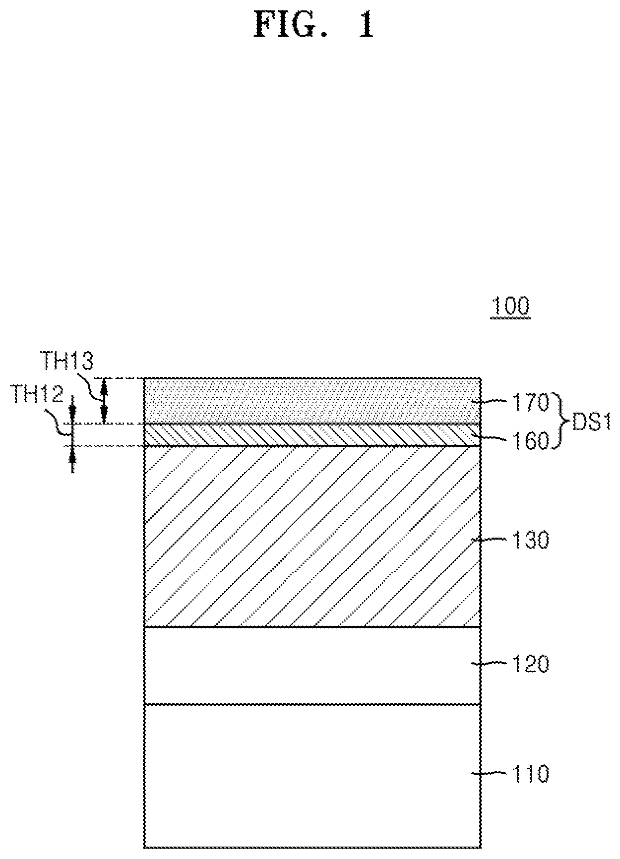
is a cross-sectional view of a main configuration of an integrated circuit device according to an embodiment.
An integrated circuit device 100 may include a substrate 110 , a lower structure 120 on the substrate 110 , a first electrode layer 130 on the lower structure 120 , and a dielectric structure DS 1 on the first electrode layer 130 . The dielectric structure DS 1 may include a first stress buffer layer 160 and a dielectric layer 170 .
The substrate 110 may include a semiconductor element, e.g., Si or Ge, or a compound semiconductor material, e.g., SiC, GaAs, InAs, or InP. The substrate 110 may include a semiconductor substrate and at least one insulation layer on the semiconductor substrate or structures including at least one conductive region. The conductive region may include a well doped with impurities or a structure doped with impurities. In an implementation, the substrate 110 may have various device isolation structures, e.g., a shallow trench isolation (STI) structure. As used herein, the term “or” is not an exclusive term, e.g., “A or B” would include A, B, or A and B.
In an implementation, the lower structure 120 may include an insulation layer. In an implementation, the lower structure 120 may include various conductive regions, e.g., a wiring layer, a contact plug, or a transistor, and insulation layers that insulate the conductive regions from one another.
The first electrode layer 130 may include a first metal and may have a first thermal expansion coefficient. The first thermal expansion coefficient of the first electrode layer 130 may be, e.g., 8.0×10 −6 /K or greater. In an implementation, the first thermal expansion coefficient of the first electrode layer 130 may be about 9.0×10 −6 /K. In an implementation, a thickness (e.g., in a direction orthogonal to a surface of the substrate 110 ) of the first electrode layer 130 may be, e.g., 100 Å or greater.
The first electrode layer 130 may include a metal film formed of the first metal, a metal nitride film including the first metal, or a combination thereof. The first metal may be a metal capable of forming a metal oxide having a rutile crystal structure as described later.
In an implementation, the first metal may be a transition metal or a post-transition metal. In an implementation, the first metal may be, e.g., Ti, Cr, Nb, Ni, Ge, Sn, Ge, Ir, Mo, Os, Pb, Ru, Sn, Ta, or W. In an implementation, the first electrode layer 130 may include Ti, Ti nitride, Cr, Cr nitride, Nb, Nb nitride, or a combination thereof. In an implementation, the first electrode layer 130 may include TiN, CrN, NbN, or a combination thereof.
As described above, the dielectric structure DS 1 including the first stress buffer layer 160 and the dielectric layer 170 may be on the first electrode layer 130 . The first stress buffer layer 160 may help reduce lattice mismatch of crystal lattices at the interface between the first electrode layer 130 and the dielectric layer 170 .
In the integrated circuit device 100 , due to the first stress buffer layer 160 , characteristics of a dielectric layer may be improved and the possibility of occurrence of a leakage current may be reduced. The dielectric structure DS 1 will be described below in more detail.
The dielectric layer 170 may be on the first electrode layer 130 . The dielectric layer 170 may include a second metal oxide including a second metal that is different from the above-described first metal. The dielectric layer 170 may have a second thermal expansion coefficient that is less than the first thermal expansion coefficient of the first electrode layer 130 .
In an implementation, the second thermal expansion coefficient of the dielectric layer 170 may be, e.g., 5.0×10 −6 /K or less. In an implementation, the second thermal expansion coefficient of the dielectric layer 170 may be about 4.0×10 −6 /K. In an implementation, a difference between the first thermal expansion coefficient of the first electrode layer 130 and the second thermal expansion coefficient of the dielectric layer 170 may be from about 3.0×10 −6 /K to about 8.0×10 −6 /K.
The second metal of the dielectric layer 170 may be a metal that is different from the first metal included in the first electrode layer 130 . In an implementation, the second metal may be Hf or Zr. In an implementation, the second metal oxide constituting the dielectric layer 170 may include hafnium oxide (HfO 2 ) or zirconium oxide (ZrO 2 ). In an implementation, a thickness TH 13 (e.g., in the direction orthogonal to a surface of the substrate 110 ) of the dielectric layer 170 may be about 10 Å to about 100 Å.
In an implementation, the second metal oxide constituting the dielectric layer 170 may be a crystalline layer. In an implementation, the second metal oxide constituting the dielectric layer 170 may be a crystalline metal oxide. The second metal oxide constituting the dielectric layer 170 may have a tetragonal crystal structure.
The first stress buffer layer 160 may be between the first electrode layer 130 and the dielectric layer 170 . The first stress buffer layer 160 may be an interposed layer between the first electrode layer 130 and the dielectric layer 170 . The first stress buffer layer 160 may be an interface layer formed at the interface between the first electrode layer 130 and the dielectric layer 170 .
The first stress buffer layer 160 may be formed by thermal stress of the first electrode layer 130 and thermal stress of the dielectric layer 170 as described below. The first stress buffer layer 160 may be formed by thermal stress due to a difference between the first thermal expansion coefficient of the first electrode layer 130 and the second thermal expansion coefficient of the dielectric layer 170 as described below. In an implementation, the first stress buffer layer 160 may include a first metal oxide including a first metal.
In an implementation, the first stress buffer layer 160 may have a rutile-shaped tetragonal crystal structure. In an implementation, the first metal may be Ti, Cr, Nb, Ni, Ge, Sn, Ge, Ir, Mo, Os, Pb, Ru, Sn, Ta, or W. In an implementation, the first metal oxide constituting the first stress buffer layer 160 may include Ti oxide, Cr oxide, Nb oxide, Ru oxide, Ni oxide, or the like.
The first metal oxide constituting the first stress buffer layer 160 may be a crystalline layer. In an implementation, the first metal oxide constituting the first stress buffer layer 160 may be a crystalline metal oxide. In an implementation, a thickness TH 12 (e.g., in the direction orthogonal to a surface of the substrate 110 ) of the first stress buffer layer 160 may be about 10 Å to about 20 Å. In an implementation, the thickness TH 12 of the first stress buffer layer 160 may be less than the thickness TH 13 of the dielectric layer 170 .
In an implementation, a lattice mismatch between the first metal oxide constituting the first stress buffer layer 160 and the second metal oxide constituting the dielectric layer 170 may be within or less than 7%. In an implementation, the first stress buffer layer 160 may include a rutile TiO 2 film, and even when the first stress buffer layer 160 has a relatively small thickness of about 10 Å, the first stress buffer layer 160 may have a relatively high dielectric constant of about 80 to about 130.
In an implementation, the first electrode layer 130 may include titanium nitride (TiN), the first stress buffer layer 160 may include TiO 2 having a rutile structure, and the dielectric layer 170 may include HfO 2 or ZrO 2 having a tetragonal crystal structure.
In an implementation, in the integrated circuit device 100 , the first stress buffer layer 160 may be at the interface between the first electrode layer 130 and the dielectric layer 170 . In an implementation, the first stress buffer layer 160 may have a rutile-shaped tetragonal crystal structure. In an implementation, the first stress buffer layer 160 may help reduce lattice mismatch of crystal lattices at the interface between the first electrode layer 130 and the dielectric layer 170 .
In an implementation, in the integrated circuit device 100 , the first stress buffer layer 160 may be between the first electrode layer 130 and the dielectric layer 170 , thereby reducing the occurrence of a leakage current and also improving the characteristics of the dielectric layer 170 .
is a cross-sectional view of a main configuration of an integrated circuit device according to an embodiment.
An integrated circuit device 200 may be the same as the integrated circuit device 100 of except that a second stress buffer layer 150 may be included in a dielectric structure DS 2 . In , reference numerals identical to those as in denote the same elements. In , descriptions of elements denoted by the same reference numerals as in may be briefly given or omitted.
The integrated circuit device 200 may include the substrate 110 , the lower structure 120 on the substrate 110 , the first electrode layer 130 on the lower structure 120 , and the dielectric structure DS 2 on the first electrode layer 130 . The dielectric structure DS 2 may include the first stress buffer layer 160 , the second stress buffer layer 150 , and the dielectric layer 170 .
The second stress buffer layer 150 may be on the first electrode layer 130 . The second stress buffer layer 150 may include a third metal oxide including a third metal that is different from the second metal of the dielectric layer 170 . The second stress buffer layer 150 may be an interface layer at the interface between the first electrode layer 130 and the first stress buffer layer 160 . The second stress buffer layer 150 may include a material different from that constituting the first stress buffer layer 160 .
The second stress buffer layer 150 may have a rutile-shaped tetragonal crystal structure that is identical to that of the first stress buffer layer 160 . The second stress buffer layer 150 may be formed by thermal stress of the first electrode layer 130 and thermal stress of the dielectric layer 170 .
The third metal of the second stress buffer layer 150 may be a transition metal or a post-transition metal. In an implementation, the third metal may be Ti, Cr, Nb, Ni, Ge, Sn, Ge, Ir, Mo, Os, Pb, Ru, Sn, Ta, or W. In an implementation, the third metal oxide constituting the second stress buffer layer 150 may include Ti oxide, Cr oxide, Nb oxide, Ru oxide, Ni oxide, etc.
The third metal oxide constituting the second stress buffer layer 150 may be a crystalline layer. In an implementation, the third metal oxide constituting the second stress buffer layer 150 may be a crystalline metal oxide. In an implementation, a thickness TH 11 of the second stress buffer layer 150 may be 10 Å or less. The thickness TH 11 of the second stress buffer layer 150 may be less than the thickness TH 12 of the first stress buffer layer 160 .
In an implementation, in the integrated circuit device 200 , the first stress buffer layer 160 and the second stress buffer layer 150 may be at the interface between the first electrode layer 130 and the dielectric layer 170 . The integrated circuit device 200 may help further reduce lattice mismatch between crystal lattices at the interface between the first electrode layer 130 and the dielectric layer 170 , thereby reducing the occurrence of a leakage current and improving the characteristics of the dielectric layer 170 .
is a cross-sectional view of a main configuration of an integrated circuit device according to an embodiment.
An integrated circuit device 300 may be the same as the integrated circuit device 100 of except that a second electrode layer 140 may be on the dielectric layer 170 . In , reference numerals identical to those as in denote the same elements. In , descriptions of elements denoted by the same reference numerals as in may be briefly given or omitted.
The integrated circuit device 300 may include the substrate 110 , the lower structure 120 on the substrate 110 , the first electrode layer 130 on the lower structure 120 , the dielectric structure DS 1 on the first electrode layer 130 , and the second electrode layer 140 on the dielectric structure DS 1 . The dielectric structure DS 1 may include the first stress buffer layer 160 and the dielectric layer 170 .
The first electrode layer 130 , the dielectric structure DS 1 , and the second electrode layer 140 may constitute a capacitor C 1 . The first electrode layer 130 may be a lower electrode layer. The second electrode layer 140 may be an upper electrode layer facing the lower electrode layer. The dielectric structure DS 1 may be between the lower electrode layer and the upper electrode layer.
The second electrode layer 140 , e.g., the upper electrode layer, may include the same material as the first electrode layer 130 , e.g., the lower electrode layer. In an implementation, the second electrode layer 140 may include a metal film formed of the first metal, a metal nitride film including the first metal, or a combination thereof.
In an implementation, the first metal of the second electrode layer 140 may be Ti, Cr, Nb, Ni, Ge, Sn, Ge, Ir, Mo, Os, Pb, Ru, Sn, Ta, or W. In an implementation, the second electrode layer 140 may include Ti, Ti nitride, Cr, Cr nitride, Nb, Nb nitride, or a combination thereof. In an implementation, the second electrode layer 140 may include TiN, CrN, NbN, or a combination thereof.
is a cross-sectional view of a main configuration of an integrated circuit device according to an embodiment.
An integrated circuit device 400 may be the same as the integrated circuit device 200 of except that the second electrode layer 140 may be on the dielectric layer 170 . In , reference numerals identical to those as in denote the same elements. In , descriptions of elements denoted by the same reference numerals as in may be briefly given or omitted.
The integrated circuit device 400 may include the substrate 110 , the lower structure 120 on the substrate 110 , the first electrode layer 130 on the lower structure 120 , the dielectric structure DS 2 on the first electrode layer 130 , and the second electrode layer 140 on the dielectric structure DS 2 . The dielectric structure DS 2 may include the first stress buffer layer 160 , the second stress buffer layer 150 , and the dielectric layer 170 .
The first electrode layer 130 , the dielectric structure DS 2 , and the second electrode layer 140 may constitute a capacitor C 2 . The first electrode layer 130 may be a lower electrode layer. The second electrode layer 140 may be an upper electrode layer facing the lower electrode layer. The dielectric structure DS 2 may be between the lower electrode layer and the upper electrode layer.
The second electrode layer 140 , e.g., the upper electrode layer, may include the same material as the first electrode layer 130 , e.g., the lower electrode layer. In an implementation, the second electrode layer 140 may include a metal film formed of the first metal, a metal nitride film including the first metal, or a combination thereof.
In an implementation, the first metal of the second electrode layer 140 may be Ti, Cr, Nb, Ni, Ge, Sn, Ge, Ir, Mo, Os, Pb, Ru, Sn, Ta, or W. In an implementation, the second electrode layer 140 may include Ti, Ti nitride, Cr, Cr nitride, Nb, Nb nitride, or a combination thereof. In an implementation, the second electrode layer 140 may include TiN, CrN, NbN, or a combination thereof.
A and 5 B are diagrams showing an arrangement of crystal lattices between a first electrode layer and a dielectric layer of an integrated circuit device according to an embodiment.
B is a diagram showing a crystal lattice arrangement of a region EL 1 of A . As described above, an integrated circuit device may include the first electrode layer 130 , the first stress buffer layer 160 , and the dielectric layer 170 .
As shown in A and 5 B , an interface IF 1 may be between a first portion including the first electrode layer 130 and the first stress buffer layer 160 and a second portion including the dielectric layer 170 . The first portion including the first electrode layer 130 and the first stress buffer layer 160 may have first crystal lattices β. The second portion including the dielectric layer 170 may have second crystal lattices α.
As shown in A and 5 B , the first stress buffer layer 160 may be present, and the integrated circuit device may have no crystal defect at the interface IF 1 between the first crystal lattices β and the second crystal lattices α, and lattice mismatch may be insignificant.
In the integrated circuit device according to an embodiment, there may be no crystal defect between the first stress buffer layer 160 and the dielectric layer 170 and lattice mismatch may be insignificant. Thus, a leakage current may be reduced and characteristics of the dielectric layer 170 may be improved.
A and 6 B are diagrams showing a lattice arrangement at an interface between a first electrode layer and a dielectric layer of an integrated circuit device according to a comparative example, for comparison with A and 5 B .
B is a diagram showing a crystal lattice arrangement of a region EL 2 of A . The integrated circuit device according to the comparative example may include a first electrode layer 130 C and a dielectric layer 170 C (e.g., directly on the first electrode layer 130 C). The first electrode layer 130 C and the dielectric layer 170 C may correspond to the first electrode layer 130 and the dielectric layer 170 , respectively.
As shown in A and 6 B , an interface IF 2 may be between a first portion including the first electrode layer 130 C and a second portion including the dielectric layer 170 C. The first portion including the first electrode layer 130 C may have first crystal lattices β′. The second portion including the dielectric layer 170 C may have second crystal lattices β′.
As shown in A and 6 B , in the integrated circuit device according to the comparative example, a crystal defect DSL (e.g., a dislocation) occurs at the interface IF 2 between the first crystal lattices β′ and the second crystal lattices α′, and lattice mismatch is significant.
In the integrated circuit device according to the comparative example, there is a crystal defect between the first electrode layer 130 C and the dielectric layer 170 C, and lattice mismatch is also significant. Therefore, a leakage current may be high and characteristics of the dielectric layer 170 C may be poor.
, 8 A, 8 B, and 9 are cross-sectional diagrams for describing a method of manufacturing an integrated circuit device, according to an embodiment.
In detail, , 8 A, 8 B, and 9 are diagrams of stages in a method of manufacturing the integrated circuit device 100 of . In , 8 A, 8 B, and 9 , a substrate ( 110 of ) and a lower structure ( 120 of ) are omitted for convenience of illustration. In , 8 A, 8 B, and 9 , reference numerals identical to those as in denote the same elements. In , 8 A, 8 B, and 9 , descriptions of elements denoted by the same reference numerals as in may be briefly given or omitted.
Referring to , the first electrode layer 130 may be formed on a lower structure ( 120 of ). The first electrode layer 130 may be formed using, e.g., chemical vapor deposition (CVD), metal organic CVD (MOCVD), physical vapor deposition (PVD), or atomic layer deposition (ALD). The first electrode layer 130 may be deposited at a temperature of about 400° C. to about 700° C. The first electrode layer 130 may include a first metal and may have a first thermal expansion coefficient.
The first thermal expansion coefficient of the first electrode layer 130 may be 8.0×10 −6 /K or higher. In an implementation, the first thermal expansion coefficient of the first electrode layer 130 may be about 9.0×10 −6 /K. In an implementation, the first electrode layer 130 may be formed to a thickness of 100 Å or greater.
The first metal may be a transition metal or a post-transition metal. The first electrode layer 130 may include a metal (e.g., non-compounded metal) film formed of the first metal, a metal nitride film including the first metal, or a combination thereof. In an implementation, the first electrode layer 130 may include TiN.
An amorphous first metal oxide 132 including the first metal may be formed on the first electrode layer 130 . The amorphous first metal oxide 132 may be obtained or formed by oxidizing a surface of the first electrode layer 130 . In an implementation, the amorphous first metal oxide 132 may be amorphous titanium oxide (TiO x ). In an implementation, the amorphous first metal oxide 132 may be formed to a thickness from about 10 Å to about 20 Å.
A and 8 B illustrate a process of crystallizing the amorphous first metal oxide 132 . B is an enlarged view of a region EL 3 of A .
As shown in A and 8 B , after the dielectric layer 170 is formed on the amorphous first metal oxide 132 , an annealing process may be performed. The dielectric layer 170 may include a second metal oxide including a second metal that is different from the above-described first metal. In an implementation, the second metal may be Hf or Zr.
In an implementation, the second metal oxide constituting the dielectric layer 170 may include HfO 2 or ZrO 2 . In an implementation, a thickness of the dielectric layer 170 may be from about 10 Å to about 100 Å. The dielectric layer 170 may be formed using, e.g., CVD, MOCVD, PVD, or ALD. In an implementation, the dielectric layer 170 may be deposited at a temperature lower than or equal to 400° C. In an implementation, the dielectric layer 170 may be annealed at a temperature of about 200° C. to about 700° C.
The dielectric layer 170 may have a second thermal expansion coefficient that is less than the first thermal expansion coefficient of the first electrode layer 130 . In an implementation, the second thermal expansion coefficient of the dielectric layer 170 may be about 4.0×10 −6 /K. In an implementation, a difference between the first thermal expansion coefficient of the first electrode layer 130 and the second thermal expansion coefficient of the dielectric layer 170 may be about 5.0×10 −6 /K.
Due to a difference between thermal expansion coefficients of the first electrode layer 130 and the dielectric layer 170 , thermal stresses 134 and 135 may be applied to the amorphous first metal oxide 132 , and crystallization of the amorphous first metal oxide 132 may occur as shown in A and 8 B .
In an implementation, tensile stress 134 may occur in the first electrode layer 130 due to the difference between thermal expansion coefficients of the first electrode layer 130 and the dielectric layer 170 . Compressive stress 135 may occur in the dielectric layer 170 due to the difference between thermal expansion coefficients of the first electrode layer 130 and the dielectric layer 170 .
The tensile stress 134 of the first electrode layer 130 and the compressive stress 135 of the dielectric layer 170 may be applied to the amorphous first metal oxide 132 . In an implementation, crystal cores 133 may be formed in the amorphous first metal oxide 132 as shown in A , and the crystal cores 133 may gradually grow as shown in B .
In an implementation, an oxygen atom 136 in the amorphous first metal oxide 132 may move to the first electrode layer 130 or the dielectric layer 170 as shown in B and may cure defects of the first electrode layer 130 and the dielectric layer 170 .
Referring to , during a process of forming the dielectric layer 170 or a process of annealing the dielectric layer 170 , the amorphous first metal oxide 132 may be crystallized to form the first stress buffer layer 160 . In an implementation, the first stress buffer layer 160 may be formed to a thickness from about 10 Å to about 20 Å. As described above, the first stress buffer layer 160 may be a crystalline layer formed by the thermal stress of the first electrode layer 130 and the thermal stress of the dielectric layer 170 .
The first stress buffer layer 160 may be formed by the thermal stress of the first electrode layer 130 and the thermal stress of the dielectric layer 170 , and the first stress buffer layer 160 may reduce lattice mismatch between the first electrode layer 130 and the dielectric layer 170 . The first stress buffer layer 160 may have a rutile-shaped tetragonal crystal structure. The first stress buffer layer 160 and the dielectric layer 170 may constitute the dielectric structure DS 1 .
In an implementation, the first stress buffer layer 160 may include the first metal oxide including the first metal. The first metal may be Ti, Cr, Nb, Ni, Ge, Sn, Ge, Ir, Mo, Os, Pb, Ru, Sn, Ta, or W.
In an implementation, the first metal oxide constituting the first stress buffer layer 160 may include Ti oxide, Cr oxide, Nb oxide, Ru oxide, Ni oxide, or the like. In an implementation, the first stress buffer layer 160 may be titanium oxide.
A and 10 B are diagrams of a crystal structure of a first stress buffer layer of an integrated circuit device according to an embodiment.
In an implementation, the first stress buffer layer ( 160 of ) of an integrated circuit device may have a rutile-shaped tetragonal crystal structure as shown in A and 10 B . In A and 10 B , for convenience of explanation, it is assumed that the first stress buffer layer ( 160 of ) includes titanium oxide.
Here, the rutile-shaped tetragonal crystal structure will be briefly described. As shown in A and 10 B , the rutile-shaped crystal structure of the first stress buffer layer ( 160 of ) may have different lattice constants in the a-axis direction and the c-axis direction.
In an implementation, in the first stress buffer layer, as shown in B , a distance between lattices of the first stress buffer layer in the a-axis direction may be about 4.59 Å, and a distance between lattices of the first stress buffer layer in the c-axis direction may be about 2.96 Å. In B , Vox may denote an oxygen vacancy.
is a diagram of lattice mismatch of an integrated circuit device according to an embodiment, and is a diagram of lattice mismatch of an integrated circuit device according to a comparative example, for comparison with the embodiment of .
is a diagram showing a case in which the first stress buffer layer 160 is formed as shown in A . is a diagram showing a lattice arrangement in which the first stress buffer layer ( 160 of A ) includes TiO 2 and the dielectric layer ( 170 of A ) includes ZrO 2 in the integrated circuit device.
As shown in , TiO 2 of the first stress buffer layer 160 on a (111) crystal plane may have a lattice constant of about 5.46 Å, and ZrO 2 of the dielectric layer 170 may have a lattice constant of about 5.09 Å.
In an implementation, a lattice mismatch between TiO 2 constituting the first stress buffer layer 160 on the (111) crystal plane and ZrO 2 constituting the dielectric layer 170 is about 7%.
is a diagram showing a case in which the first stress buffer layer 160 is not formed, e.g., as shown in A . is a diagram showing a lattice arrangement in which the first electrode layer ( 130 C of A ) includes TiN and the dielectric layer ( 170 C of A ) includes ZrO 2 in the integrated circuit device according to the comparative example.
As shown in , TiN of the first electrode layer 130 C on the (111) crystal plane may have a lattice constant of about 5.99 Å, and ZrO 2 of the dielectric layer 170 may have a lattice constant of about 5.09 Å.
A lattice mismatch between TiN constituting the first electrode layer 130 C on the (111) crystal plane and ZrO 2 of the dielectric layer 170 C is about 17%. As described above, when an integrated circuit device includes the first stress buffer layer 160 , lattice mismatch between the first stress buffer layer 160 and the dielectric layer 170 may be reduced.
is a graph showing capacitance characteristics of an integrated circuit device according to an embodiment.
is a graph showing capacitance characteristics of the integrated circuit device 300 of and the integrated circuit device 400 of . IN 1 represents the capacitance characteristics of the integrated circuit device 300 of .
IN 2 represents the capacitance characteristics of the integrated circuit device 400 of . RE relates to an integrated circuit device according to a comparative example, and, in , RE indicates that the first stress buffer layer 160 and the second stress buffer layer 150 are not formed.
As shown in , the integrated circuit device 300 including the first stress buffer layer 160 exhibits higher capacitance than the integrated circuit device (represented by RE) of the comparative example as indicated by IN 1 , and the dielectric layer ( 170 of ) exhibits good characteristics. Also, it may be seen that, the integrated circuit device 400 including the first stress buffer layer 160 and the second stress buffer layer 150 exhibits higher capacitance than the integrated circuit device (represented by RE) of the comparative example as indicated by IN 2 , and the dielectric layer ( 170 of ) exhibits good characteristics.
Furthermore, it may be seen that the integrated circuit device 400 including the first stress buffer layer 160 and the second stress buffer layer 150 exhibits higher capacitance than an integrated circuit device (indicated by IN 1 ) in the integrated circuit device 300 including only the first stress buffer layer 160 as indicated by IN 2 , and the dielectric layer ( 170 of ) exhibits better characteristics.
is a graph showing concentrations of first and second stress buffer layers according to depths in an integrated circuit device according to an embodiment.
shows concentration profiles PL 1 , PL 2 , and PL 3 of a first stress buffer layer ( 160 of ) and a second stress buffer layer ( 150 of ) according to depths from surfaces SR of dielectric layers 170 of the integrated circuit device 100 of and the integrated circuit device 200 of .
As shown in , the concentrations of oxygen atoms in the first stress buffer layer ( 160 of ) and the second stress buffer layer ( 150 of ) may have a maximum value at a predetermined depth from the surface SR of the dielectric layer 170 as indicated by PL 3 .
A concentration of titanium atoms in the first stress buffer layer ( 160 of ) may have a maximum value at a predetermined depth from the surface SR of the dielectric layer 170 as indicated by PL 1 . A concentration of titanium atoms in the second stress buffer layer ( 150 of ) may have a maximum value at a predetermined depth from the surface SR of the dielectric layer 170 as indicated by PL 2 . The predetermined depth indicated by PL 2 may be greater, e.g., deeper, than the predetermined depth indicated by PL 1 . The concentration of titanium atoms in the first stress buffer layer ( 160 of ) and the second stress buffer layer ( 150 of ) may be higher than the concentration of oxygen atoms.
A is a cross-sectional diagram of an integrated circuit device according to an embodiment, and B is an enlarged cross-sectional view of a region Q 1 in A .
In A and 15 B , reference numerals identical to those as in denote the same elements. In A and 15 B , descriptions of elements denoted by the same reference numerals as in may be briefly given or omitted.
An integrated circuit device 500 may include a substrate 610 , which includes a plurality of active regions AC, and an interlayer insulation layer 620 on the substrate 610 . A plurality of conductive regions 624 may penetrate through the interlayer insulation layer 620 and be connected to the active regions AC.
The substrate 610 may have substantially the same configuration as that described for the substrate 110 with reference to . The active regions AC may be defined by a plurality of device isolation regions 612 in the substrate 610 . A device isolation region 612 may include an oxide film, a nitride film, or a combination thereof. The interlayer insulation layer 620 may include a silicon oxide layer. The conductive region 624 may include poly-silicon, a metal, conductive metal nitride, metal silicide, or a combination thereof.
An insulation pattern 626 P having a plurality of openings 626 H may be on the interlayer insulation layer 620 and the conductive regions 624 . The insulation pattern 626 P may include silicon nitride, silicon oxynitride, or a combination thereof.
A plurality of capacitors C 3 may be on the conductive regions 624 . The capacitors C 3 may include a lower electrode layer 630 and an upper electrode layer 640 . The capacitors C 3 may share one upper electrode layer 640 . The lower electrode layers 630 may each have a cylindrical shape or a cup shape with a closed bottom surface facing the substrate 610 . More detailed configurations of the lower electrode layer 630 and the upper electrode layer 640 are substantially the same as those of the first electrode layer 130 and the second electrode layer 140 described with reference to , respectively.
Each of the capacitors C 3 may further include the dielectric structure DS 1 between the lower electrode layer 630 and the upper electrode layer 640 . The dielectric structure DS 1 may include the first stress buffer layer 160 and the dielectric layer 170 . The first stress buffer layer 160 and the dielectric layer 170 may be substantially the same as those described with reference to , respectively.
The first stress buffer layer 160 may cover the surfaces of the lower electrode layers 630 . The dielectric layer 170 may continuously extend on the substrate 610 to cover the surface of the first stress buffer layer 160 and to cover the top surface of the insulation pattern 626 P between the lower electrode layers 630 . The upper electrode layer 640 may cover the dielectric layer 170 .
The dielectric structure DS 1 of the capacitors C 3 in the integrated circuit device 500 described with reference to A and 15 B may include the first stress buffer layer 160 and the dielectric layer 170 sequentially stacked on the lower electrode layer 630 . The bottom surface of the first stress buffer layer 160 may be in contact (e.g., direct contact) with the lower electrode layer 630 , and the top surface of the first stress buffer layer 160 may be in contact (e.g., direct contact) with the dielectric layer 170 .
As described above, the first stress buffer layer 160 may be formed by thermal stress of the lower electrode layer 630 and thermal stress of the dielectric layer 170 . In the integrated circuit device 500 , the first stress buffer layer 160 may be between the lower electrode layer 630 and the dielectric layer 170 , thereby reducing the occurrence of a leakage current and also improving the characteristics of the dielectric layer 170 .
A is a cross-sectional diagram of an integrated circuit device according to an embodiment, and B is an enlarged cross-sectional view of a region Q 2 in A .
In A and 16 B , reference numerals identical to those as in , 4 , 15 A, and 15 B denote the same elements. In A and 16 B , descriptions of elements denoted by the same reference numerals as in , 4 , 15 A, and 15 B may be briefly given or omitted.
An integrated circuit device 600 may include the substrate 610 , which includes the active regions AC, and the interlayer insulation layer 620 on the substrate 610 . An insulation pattern 626 P having a plurality of openings 626 H may be on the interlayer insulation layer 620 and the conductive regions 624 .
A plurality of capacitors C 4 may be on the conductive regions 624 . The capacitors C 4 may include the lower electrode layer 630 and the upper electrode layer 640 . The lower electrode layers 630 may each have a cylindrical shape or a cup shape with a closed bottom surface facing the substrate 610 . More detailed configurations of the lower electrode layer 630 and the upper electrode layer 640 are substantially the same as those of the first electrode layer 130 and the second electrode layer 140 described with reference to , respectively.
Each of the capacitors C 4 may further include the dielectric structure DS 2 between the lower electrode layer 630 and the upper electrode layer 640 . The dielectric structure DS 2 may include the second stress buffer layer 150 , the first stress buffer layer 160 , and the dielectric layer 170 . The second stress buffer layer 150 , the first stress buffer layer 160 , and the dielectric layer 170 may be substantially the same as those described with reference to , respectively.
The second stress buffer layer 150 may cover the surfaces of the lower electrode layers 630 . The first stress buffer layer 160 may cover the surface of the second stress buffer layer 150 . The dielectric layer 170 may continuously extend on the substrate 610 and may cover the surface of the first stress buffer layer 160 and the top surface of the insulation pattern 626 P between the lower electrode layers 630 . The upper electrode layer 640 may cover the dielectric layer 170 .
The dielectric structure DS 2 of the capacitors C 4 in the integrated circuit device 600 described with reference to A and 16 B may include the second stress buffer layer 150 , the first stress buffer layer 160 , and the dielectric layer 170 sequentially stacked on the lower electrode layer 630 . The bottom surface of the second stress buffer layer 150 is in contact with the lower electrode layer 630 , and the top surface of the second stress buffer layer 150 may be in contact (e.g., direct contact) with the first stress buffer layer 160 . The bottom surface of the first stress buffer layer 160 is in contact with the second stress buffer layer 150 , and the top surface of the first stress buffer layer 160 may be in contact (e.g., direct contact) with the dielectric layer 170 .
As described above, the second stress buffer layer 150 and the first stress buffer layer 160 may be formed by thermal stress of the lower electrode layer 630 and thermal stress of the dielectric layer 170 . In the integrated circuit device 600 , the second stress buffer layer 150 and the first stress buffer layer 160 may be between the lower electrode layer 630 and the dielectric layer 170 , thereby reducing the occurrence of a leakage current and also improving the characteristics of the dielectric layer 170 .
A is a cross-sectional diagram of an integrated circuit device according to an embodiment, and B is an enlarged cross-sectional view of a region Q 3 in A .
In A and 17 B , reference numerals identical to those as in , 3 , 15 A, and 15 B denote the same elements. In A and 17 B , descriptions of elements denoted by the same reference numerals as in , 3 , 15 A, and 15 B may be briefly given or omitted.
An integrated circuit device 700 may include the substrate 610 , which includes the active regions AC, and the interlayer insulation layer 620 on the substrate 610 . An insulation pattern 626 P having a plurality of openings 626 H may be on the interlayer insulation layer 620 and the conductive regions 624 .
A plurality of capacitors C 5 may be on the conductive regions 624 . The capacitors C 5 may include a lower electrode layer 830 and an upper electrode layer 840 . The capacitors C 5 may share one upper electrode layer 840 . Each of the lower electrode layers 830 may have a pillar shape. More detailed configurations of the lower electrode layer 830 and the upper electrode layer 840 are substantially the same as those of the first electrode layer 130 and the second electrode layer 140 described with reference to , respectively.
Each of the capacitors C 5 may further include the dielectric structure DS 1 between the lower electrode layer 830 and the upper electrode layer 840 . The dielectric structure DS 1 may include the first stress buffer layer 160 and the dielectric layer 170 . The first stress buffer layer 160 and the dielectric layer 170 may be substantially the same as those described with reference to , respectively.
The first stress buffer layer 160 may cover the surfaces of the lower electrode layers 830 . The dielectric layer 170 may continuously extend on the substrate 610 and may cover the surface of the first stress buffer layer 160 and the top surface of the insulation pattern 626 P between the lower electrode layers 830 . The upper electrode layer 840 may cover the dielectric layer 170 .
The dielectric structure DS 1 of the capacitors C 5 in the integrated circuit device 700 described with reference to A and 17 B may include the first stress buffer layer 160 and the dielectric layer 170 sequentially stacked on the lower electrode layer 830 . The bottom surface of the first stress buffer layer 160 may be in contact (e.g., direct contact) with the lower electrode layer 830 , and the top surface of the first stress buffer layer 160 may be in contact (e.g., direct contact) with the dielectric layer 170 .
As described above, the first stress buffer layer 160 may be formed by thermal stress of the lower electrode layer 830 and thermal stress of the dielectric layer 170 . In the integrated circuit device 700 , the first stress buffer layer 160 may be between the lower electrode layer 830 and the dielectric layer 170 , thereby reducing the occurrence of a leakage current and also improving the characteristics of the dielectric layer 170 .
A is a cross-sectional diagram of an integrated circuit device according to an embodiment, and B is an enlarged cross-sectional view of a region Q 4 in A .
In A and 18 B , reference numerals identical to those as in , 4 , 17 A, and 17 B denote the same elements. In A and 18 B , descriptions of elements denoted by the same reference numerals as in , 4 , 17 A, and 17 B may be briefly given or omitted.
An integrated circuit device 800 may include the substrate 610 , which includes the active regions AC, and the interlayer insulation layer 620 on the substrate 610 . An insulation pattern 626 P having a plurality of openings 626 H may be on the interlayer insulation layer 620 and the conductive regions 624 .
A plurality of capacitors C 6 may be on the conductive regions 624 . The capacitors C 6 may include the lower electrode layer 830 and the upper electrode layer 840 . Each of the lower electrode layers 830 may have a pillar shape. More detailed configurations of the lower electrode layer 830 and the upper electrode layer 840 are substantially the same as those of the first electrode layer 130 and the second electrode layer 140 described with reference to , respectively.
Each of the capacitors C 6 may further include the dielectric structure DS 2 between the lower electrode layer 830 and the upper electrode layer 840 . The dielectric structure DS 2 may include the second stress buffer layer 150 , the first stress buffer layer 160 , and the dielectric layer 170 . The second stress buffer layer 150 , the first stress buffer layer 160 , and the dielectric layer 170 may be substantially the same as those described with reference to , respectively.
The second stress buffer layer 150 may cover the surfaces of the lower electrode layers 830 . The first stress buffer layer 160 may cover the surface of the second stress buffer layer 150 . The dielectric layer 170 may continuously extend on the substrate 610 and may cover the surface of the first stress buffer layer 160 and the top surface of the insulation pattern 626 P between the lower electrode layers 830 . The upper electrode layer 840 may cover the dielectric layer 170 .
The dielectric structure DS 2 of the capacitors C 6 in the integrated circuit device 800 described with reference to A and 18 B may include the second stress buffer layer 150 , the first stress buffer layer 160 , and the dielectric layer 170 sequentially stacked on the lower electrode layer 630 . The bottom surface of the second stress buffer layer 150 may be in contact (e.g., direct contact) with the lower electrode layer 830 , and the top surface of the second stress buffer layer 150 may be in contact (e.g., direct contact) with the first stress buffer layer 160 . The bottom surface of the first stress buffer layer 160 may be in contact (e.g., direct contact) with the second stress buffer layer 150 , and the top surface of the first stress buffer layer 160 may be in contact (e.g., direct contact) with the dielectric layer 170 .
As described above, the second stress buffer layer 150 and the first stress buffer layer 160 may be formed by thermal stress of the lower electrode layer 830 and thermal stress of the dielectric layer 170 . In the integrated circuit device 800 , the second stress buffer layer 150 and the first stress buffer layer 160 may be between the lower electrode layer 830 and the dielectric layer 170 , thereby reducing the occurrence of a leakage current and also improving the characteristics of the dielectric layer 170 .
A to 19 I are cross-sectional diagrams of stages in a method of manufacturing an integrated circuit device, according to an embodiment.
An example method of manufacturing the integrated circuit device 500 shown in A and 15 B will be described with reference to A to 19 I . In A to 19 I , reference numerals identical to those as in A and 15 B denote the same elements. In A to 19 I , descriptions of elements denoted by the same reference numerals as in A and 15 B may be briefly given or omitted.
Referring to A , the interlayer insulation layer 620 may be formed on the substrate 610 in which the active regions AC are defined by the device isolation region 612 . Next, the conductive regions 624 penetrating through the interlayer insulation layer 620 and connected to the active regions AC may be formed.
Referring to B , an insulation layer 626 and a mold layer 628 may be sequentially formed on the interlayer insulation layer 620 and the conductive regions 624 . The insulation layer 626 may be an etch stop layer. The insulation layer 626 may include an insulating material having an etch selectivity with respect to the interlayer insulation layer 620 and the mold layer 628 . In an implementation, the insulation layer 626 may include silicon nitride, silicon oxynitride, or a combination thereof.
The mold layer 628 may include an oxide layer. In an implementation, the mold layer 628 may include at least one supporting layer. At least one supporting layer may include a material having an etching selectivity with respect to the mold layer 628 .
Referring to C , a sacrificial layer SL and a mask pattern MP may be sequentially formed on the mold layer 628 . The sacrificial layer SL may include an oxide layer. The mask pattern MP may include an oxide layer, a nitride layer, a poly-silicon layer, a photoresist layer, or a combination thereof. A region in which a lower electrode layer of a capacitor is to be formed may be defined by the mask pattern MP.
Referring to D , from the result of C , a sacrificial pattern SLP, a mold pattern 628 P, and the insulation pattern 626 P may be formed by anisotropically etching the sacrificial layer SL, the mold layer 628 , and the insulation layer 626 using the mask pattern MP as an etching mask and the insulation layer 626 as an etch stop layer. A plurality of openings 626 H exposing the conductive regions 624 may be formed in the insulation pattern 626 P.
Referring to E , after removing the mask pattern MP from the result of D , a conductive layer 630 L covering surfaces of the conductive regions 624 , the surface of the insulation pattern 626 P, the surface of the mold pattern 628 P, and the surface of the sacrificial pattern SLP may be formed inside a plurality of holes BEH, respectively. The conductive layer 630 L may be a lower electrode layer after a subsequent process. The conductive layer 630 L may be formed to conformally cover the inner sidewalls of the holes BEH, such that the inner space of each of the holes BEH partially remains.
A material of the conductive layer 630 L may be the same as the material of the first electrode layer 130 described with reference to . To form the conductive layer 630 L, a CVD process, an MOCVD process, or an ALD process may be used.
Referring to F , the conductive layer 630 L may be separated into the lower electrode layers 630 by partially removing the upper portion of the conductive layer 630 L from the result of E . In order to form the lower electrode layers 630 , a portion of the conductive layer 630 L and a sacrificial pattern (SLP of E ) may be removed through an etch back process or a chemical mechanical polishing (CMP) process so that the top surface of the mold pattern 628 P is exposed.
Referring to G , the mold pattern 628 P may be removed from the result of F , and the outer surfaces of the lower electrode layers 630 having a cylindrical shape and the top surface of the insulation pattern 626 P are exposed.
Referring to H , a stress buffer material layer 160 ′ may be formed on a surface of each of the lower electrode layers 630 by oxidizing the exposed surface of each of the lower electrode layers 630 . The stress buffer material layer 160 ′ may be an amorphous metal oxide layer. The stress buffer material layer 160 ′ may be the amorphous first metal oxide 132 of .
In an implementation, the stress buffer material layer 160 ′ may be formed by performing a heat treatment on the lower electrode layers 630 at a temperature from about 100° C. to about 600° C. under an oxidizing atmosphere. The heat treatment may be, e.g., a rapid thermal annealing (RTA) process, an annealing process, a plasma annealing process, or a combination thereof.
In an implementation, the stress buffer material layer 160 ′ may be formed by supplying an oxidizing reaction gas to the exposed surfaces of the lower electrode layers 630 . The oxidizing reaction gas may include, e.g., O 2 , O 3 , H 2 O, NO, NO 2 , N 2 O, CO 2 , H 2 O 2 , HCOOH, CH 2 COOH, plasma O 2 , remote plasma O 2 , plasma N 2 O, plasma H 2 O, or a combination thereof.
Referring to I , the dielectric layer 170 may be sequentially formed on the result of H on which the stress buffer material layer 160 ′ has been formed. In an implementation, an ALD process may be used to form the dielectric layer 170 . After the dielectric layer 170 is formed, a result structure with the dielectric layer 170 may be annealed.
During a process of forming the dielectric layer 170 or a process of annealing the dielectric layer 170 , the stress buffer material layer 160 ′ may be crystallized to form the first stress buffer layer 160 . The dielectric structure DS 1 including the first stress buffer layer 160 and the dielectric layer 170 may be formed.
As described above, the first stress buffer layer 160 may be formed as the stress buffer material layer 160 ′ is crystallized by thermal stress of the lower electrode layer 630 and thermal stress of the dielectric layer 170 . The process of forming the first stress buffer layer 160 is as described above with reference to A, 8 B, and 9 . Subsequently, an upper electrode layer ( 640 of A and 15 B ) may be formed on a result structure on which the dielectric structure DS 1 is formed, thereby completing the manufacture of the integrated circuit device ( 500 of A and 15 B ).
By way of summation and review, in an integrated circuit device, if the characteristics of a dielectric layer were poor, a leakage current could occur or desired electrical characteristics may not be obtained. Moreover, a thickness of a dielectric layer may be decreased as an integrated circuit device becomes highly integrated, and a structure may be capable of improving the characteristics of the dielectric layer.
One or more embodiments may provide an integrated circuit device including a dielectric layer.
One or more embodiments may provide an integrated circuit device capable of improving the characteristics of a dielectric layer.
Example embodiments have been disclosed herein, and although specific terms are employed, they are used and are to be interpreted in a generic and descriptive sense only and not for purpose of limitation. In some instances, as would be apparent to one of ordinary skill in the art as of the filing of the present application, features, characteristics, and/or elements described in connection with a particular embodiment may be used singly or in combination with features, characteristics, and/or elements described in connection with other embodiments unless otherwise specifically indicated. Accordingly, it will be understood by those of skill in the art that various changes in form and details may be made without departing from the spirit and scope of the present invention as set forth in the following claims.
Figures (20)
Citations
This patent cites (9)
- US7735206
- US8486780
- US9978753
- US20090273882
- US20170200782
- US20200091279
- US20210142946
- US2434529
- US10-2013-0123183