Semiconductor Device Including a Circuit for Transmitting a Signal
Abstract
Reliability of a semiconductor device is improved. The semiconductor device PKG 1 includes a wiring substrate SUB 1, a semiconductor chip CHP 1 and a capacitor CDC mounted on the upper surface 2 t of the wiring substrate SUB 1, and a lid LD formed of a metallic plate covering the semiconductor chip CHP 1 and the wiring substrate SUB 1. The semiconductor chip CHP 1 is bonded to the lid LD via a conductive adhesive layer, and the capacitor CDC, which is thicker than the thickness of the semiconductor chip CHP 1, is disposed in the cut off portion 4 d 1 provided in the lid LD, and is exposed from the lid LD.
Claims (16)
1. A semiconductor device comprising: a wiring substrate having a first main surface and a second main surface opposite the first main surface, the first main surface having a central portion and a peripheral portion surrounding the central portion in plan view; a semiconductor chip having a front surface and a rear surface opposite the front surface, the semiconductor chip being mounted on the central portion of the first main surface of the wiring substrate; a first capacitor mounted on the peripheral portion of the first main surface of the wiring substrate; and a lid disposed over the first main surface of the wiring substrate such that the lid covers the semiconductor chip, the lid having a heat radiation portion and a flange portion surrounding the heat radiating portion, wherein in plan view, the first main surface of the wiring substrate has a rectangular shape comprised of: a first side extending in a first direction; a second side opposite the first side and extending in the first direction; a third side extending in a second direction perpendicular to the first direction; and a fourth side opposite the third side and extending in the second direction, wherein in plan view, the peripheral portion of the first main surface of the wiring substrate has: a first corner portion including a first corner defined by the first side and the third side; a second corner portion including a second corner defined by the third side and the second side; a third corner portion including a third corner defined by the second side and the fourth side; a fourth corner portion including a fourth corner defined by the fourth side and the first side; a first middle portion located between the first corner portion and the second corner portion, in the second direction; a second middle portion located between the second corner portion and the third corner portion, in the first direction; a third middle portion located between the third corner portion and the fourth corner portion, in the second direction; and a fourth middle portion located between the fourth corner portion and the first corner portion, in the first direction, wherein the flange portion of the lid is bonded to the wiring substrate via a first adhesive layer at each corner portion of the peripheral portion of the first main surface of the wiring substrate, wherein the first capacitor is mounted on the first middle portion of the peripheral portion of the first main surface of the wiring substrate, wherein the semiconductor chip is mounted on the central portion of the first main surface of the wiring substrate such that the front surface of the semiconductor chip faces the first main surface of the wiring substrate, wherein the heat radiation portion of the lid is bonded to the rear surface of the semiconductor chip via a second adhesive layer, wherein a thickness of the semiconductor chip is thinner than a thickness of the first capacitor, wherein in cross-sectional view, a mounting height of the first capacitor from the first main surface of the wiring substrate is higher than a mounting height of the semiconductor chip from the first main surface of the wiring substrate, wherein in plan view, the lid has a first notched portion concaved from a peripheral edge of the lid toward the heat radiation portion in plan view, and wherein the lid is disposed over the first main surface of the wiring substrate such that the first capacitor is exposed from the lid at the first notched portion.
15. A semiconductor device comprising: a wiring substrate having a first main surface and a second main surface opposite the first main surface, the first main surface having a central portion and a peripheral portion surrounding the central portion in plan view; a semiconductor chip having a front surface and a rear surface opposite the front surface, the semiconductor chip being mounted on the central portion of the first main surface of the wiring substrate; a fifth capacitor mounted on the central portion of the first main surface of the wiring substrate; and a lid disposed over the first main surface of the wiring substrate such that the lid covers the semiconductor chip, the lid having a heat radiation portion and a flange portion surrounding the heat radiating portion, wherein in plan view, the first main surface of the wiring substrate has a rectangular shape comprised of: a first side extending in a first direction; a second side opposite the first side and extending in the first direction; a third side extending in a second direction perpendicular to the first direction; and a fourth side opposite the third side and extending in the second direction, wherein in plan view, the peripheral portion of the first main surface of the wiring substrate has: a first corner portion including a first corner defined by the first side and the third side; a second corner portion including a second corner defined by the third side and the second side; a third corner portion including a third corner defined by the second side and the fourth side; a fourth corner portion including a fourth corner defined by the fourth side and the first side; a first middle portion located between the first corner portion and the second corner portion, in the second direction; a second middle portion located between the second corner portion and the third corner portion, in the first direction; a third middle portion located between the third corner portion and the fourth corner portion, in the second direction; and a fourth middle portion located between the fourth corner portion and the first corner portion, in the first direction, wherein the flange portion of the lid is bonded to the wiring substrate via a first adhesive layer at each corner portion of the peripheral portion of the first main surface of the wiring substrate, wherein the semiconductor chip is mounted on the central portion of the first main surface of the wiring substrate such that the front surface of the semiconductor chip faces the first main surface of the wiring substrate, wherein the heat radiation portion of the lid is bonded to the rear surface of the semiconductor chip via a second adhesive layer, wherein a thickness of the semiconductor chip is thinner than a thickness of the fifth capacitor, wherein in cross-sectional view, a mounting height of the fifth capacitor from the first main surface of the wiring substrate is higher than a mounting height of the semiconductor chip from the first main surface of the wiring substrate, wherein in plan view, the lid has a first opening portion provided in the heat radiation portion, and wherein the lid is disposed over the first main surface of the wiring substrate such that the fifth capacitor is exposed from the lid at the first opening portion.
Show 14 dependent claims
2. The semiconductor device according to claim 1 , further comprising a second capacitor mounted on the third middle portion of the peripheral portion of the first main surface of the wiring substrate.
3. The semiconductor device according to claim 2 , wherein the thickness of the semiconductor chip is thinner than a thickness of the second capacitor, wherein in cross-sectional view, a mounting height of the second capacitor from the first main surface of the wiring substrate is higher than the mounting height of the semiconductor chip from the first main surface of the wiring substrate, wherein in plan view, the lid further has: a second notched portion concaved from the peripheral edge of the lid toward the heat radiation portion in plan view, and wherein the lid is disposed over the first main surface of the wiring substrate such that the first capacitor is exposed from the lid at the first notched portion and such that the second capacitor is exposed from the lid at the second notched portion.
4. The semiconductor device according to claim 3 , further comprising: a third capacitor mounted on the second middle portion of the peripheral portion of the first main surface of the wiring substrate; and a fourth capacitor mounted on the fourth middle portion of the peripheral portion of the first main surface of the wiring substrate.
5. The semiconductor device according to claim 4 , wherein the thickness of the semiconductor chip is thinner than a thickness of each of the third through fourth capacitors, wherein in cross-sectional view, a mounting height of each of the third through fourth capacitors from the first main surface of the wiring substrate is higher than the mounting height of the semiconductor chip from the first main surface of the wiring substrate, wherein in plan view, the lid has: a third notched portion concaved from the peripheral edge of the lid toward the heat radiation portion in plan view; and a fourth notched portion concaved from the peripheral edge of the lid toward the heat radiation portion in plan view, and wherein the lid is disposed over the first main surface of the wiring substrate such that the third capacitor is exposed from the lid at the third notched portion and such that the fourth capacitor is exposed from the lid at the fourth notched portion.
6. The semiconductor device according to claim 5 , wherein each of the first capacitor and the second capacitor is a DC (Direct Current) cutting capacitor, and wherein each of the third capacitor and the fourth capacitor is a bypass capacitor.
7. The semiconductor device according to claim 6 , wherein each of the first adhesive layer and the second adhesive layer is made of a conductive material, and wherein the flange portion of the lid is connected to an electrode of the wiring substrate via the first adhesive layer, a reference potential being to be applied to the electrode.
8. The semiconductor device according to claim 4 , wherein the thickness of the semiconductor chip is thinner than a thickness of each of the third through fourth capacitors, wherein in cross-sectional view, a mounting height of each of the third through fourth capacitors from the first main surface of the wiring substrate is higher than the mounting height of the semiconductor chip from the first main surface of the wiring substrate, wherein in plan view, the lid has a first opening portion and a second opening portion, and wherein the lid is disposed over the first main surface of the wiring substrate such that the third capacitor is exposed from the lid at the first opening portion and such that the fourth capacitor is exposed from the lid at the second opening portion.
9. The semiconductor device according to claim 8 , wherein each of the first capacitor and the second capacitor is a DC (Direct Current) cutting capacitor, and wherein each of the third capacitor and the fourth capacitor is a bypass capacitor.
10. The semiconductor device according to claim 9 , wherein each of the first adhesive layer and the second adhesive layer is made of a conductive material, and wherein the flange portion of the lid is connected to an electrode of the wiring substrate via the first adhesive layer, a reference potential being to be applied to the electrode.
11. The semiconductor device according to claim 1 , further comprising: a fifth capacitor mounted on the central portion of the first main surface of the wiring substrate, wherein a thickness of the semiconductor chip is thinner than a thickness of the fifth capacitor, wherein in cross-sectional view, a mounting height of the fifth capacitor from the first main surface of the wiring substrate is higher than a mounting height of the semiconductor chip from the first main surface of the wiring substrate, wherein in plan view, the lid has a first opening portion provided in the heat radiation portion, and wherein the lid is disposed over the first main surface of the wiring substrate such that the fifth capacitor is exposed from the lid at the first opening portion.
12. The semiconductor device according to claim 11 , wherein the first capacitor is a DC (Direct Current) cutting capacitor, and wherein the fifth capacitor is a bypass capacitor.
13. The semiconductor device according to claim 12 , wherein the first adhesive layer is made of a conductive material, and wherein the flange portion of the lid is connected to an electrode of the wiring substrate via the first adhesive layer, a reference potential being to be applied to the electrode.
14. The semiconductor device according to claim 1 , wherein the first adhesive layer is made of a conductive material, and wherein the flange portion of the lid is connected to an electrode of the wiring substrate via the first adhesive layer, a reference potential being to be applied to the electrode.
16. The semiconductor device according to claim 15 , wherein the fifth capacitor is a bypass capacitor.
Full Description
Show full text →
CROSS-REFERENCE TO RELATED APPLICATIONS
This is a Continuation of U.S. patent application Ser. No. 16/444,933 filed on Jun. 18, 2019, which claims the benefit of Japanese Patent Application No. 2018-122161 filed on Jun. 27, 2018 including the specification, drawings and abstract are incorporated herein by reference in their entirety.
TECHNICAL FIELD OF THE INVENTION
The present invention relates to a semiconductor device, and, for example, to a technology effective for application to a semiconductor device including a circuit for transmitting a signal at high speed.
BACKGROUND OF THE INVENTION
In Japanese Patent Application publication No. 2000-311960, there is disclosed a semiconductor device having a structure in which a semiconductor chip and a capacitor mounted on a wiring substrate are covered with a cap, and a heat sink having fins is attached to a top wall of the cap.
In of WO Patent Application Publication No. 2015-162768, there is disclosed a semiconductor device having a structure in which a semiconductor chip, a capacitor for a power supply circuit, and a capacitor for a DC circuit are mounted on a wiring substrate is described.
The semiconductor chip and the capacitor for the power supply circuit are covered with the heat radiating plate, and the capacitor for the DC circuit is not covered with the heat radiating plate but is disposed in a region outside the heat radiating plate.
SUMMARY OF THE INVENTION
The semiconductor device examined by the inventor of the present application has a wiring substrate, a semiconductor chip and a plurality of capacitors mounted on the wiring substrate, and a lid covering the semiconductor chip and the plurality of capacitors, which corresponds to the cap or the heat sink described above.
The semiconductor chip is flip-chip connected to the wiring substrate.
That is, the surface of the semiconductor chip is disposed facing the wiring substrate, and is connected to the pads (terminals) of the wiring substrate via the protruding electrodes.
A lid is attached to the back surface of the semiconductor chip via an adhesive layer.
The plurality of capacitors are arranged in a space between the wiring board and the lid, and the two terminals of the capacitor are respectively connected to the two electrodes of the wiring board, but a gap is provided between the metal lid and the capacitor so that the two terminals of the capacitor are not short-circuited.
Therefore, the thickness of the semiconductor chip is equal to or larger than the thickness of the capacitor.
The semiconductor chip investigated by the inventor of the present application uses a low-k film having low mechanical strength as an interlayer insulating film for separating a plurality of wiring layers provided on a semiconductor substrate.
Here, the Low-k film is defined as an insulating film having a relative dielectric constant of 3.7 or less.
When a semiconductor chip using a Low-k film is flip-chip connected, a problem has been confirmed that thermal stress is applied to the protruding electrodes due to a difference in thermal expansion coefficient between a semiconductor substrate made of silicon and a wiring substrate, and cracks occur in an interlayer insulating film (Low-k film) having low mechanical strength.
In order to prevent the occurrence of such cracks, the inventors of the present application have investigated thinning the thickness of the semiconductor chip.
However, the inventors of the present application have confirmed that, when the semiconductor chip is thinned, the gap described above is eliminated, the two terminals of the capacitor are short-circuited by the metal lid, the functional characteristic of the semiconductor device is defective, and the reliability is lowered.
That is, in a semiconductor device in which a semiconductor chip and a capacitor are mounted on a wiring substrate, a technique for improving reliability is required.
Other objects and novel features will become apparent from the description of this specification and the accompanying drawings.
A semiconductor device according to an embodiment includes: a wiring substrate including a first main surface including a first side extending in a first direction; a second main surface opposite to the first main surface; and a first external electrode disposed on a second main surface; a semiconductor chip including a first front surface, a first back surface opposite to the first front surface, and a first electrode disposed on the first front surface, and mounted on the wiring substrate such that the first front surface faces the first main surface; a first capacitor mounted on the first main surface in a region different from the region in which the semiconductor chip is mounted, and including a first terminal and a second terminal; and a lid bonded to the first back surface of the semiconductor chip via a first adhesive layer and covering the first main surface of the wiring substrate.
The first electrode of the semiconductor chip is connected to the first terminal of the first capacitor, the second terminal of the first capacitor is connected to the first external terminal of the wiring board, the thickness of the semiconductor chip is thinner than the thickness of the first capacitor and includes a second side extending in the first direction of the lid, the second side extending along the first side of the wiring board, and the first capacitor is disposed in the first notched portion provided on the second side of the lid and exposed from the lid.
According to the above embodiment, the reliability of the semiconductor device can be improved.
BRIEF DESCRIPTIONS OF THE DRAWINGS
is an explanatory diagram showing a configuration example of an electronic device.
is an explanatory diagram showing a configuration example of a circuit included in the electronic device shown in .
is a top view of one of the two semiconductor devices shown in .
is cross-sectional view of a wiring substrate constituting the semiconductor device shown in .
is a bottom view of the semiconductor device shown in .
is plan view of an electrode arrangement surface of the semiconductor chip shown in .
is cross-sectional view of a main part along line X 1 -X 1 ′ of .
is a cross-sectional view of a main part along line X 2 -X 2 ′ of .
is a cross-sectional view of a main part along line Y 1 -Y 1 ′ of .
is plan view of wiring for connecting electrodes of a semiconductor chip and solder balls on a wiring substrate.
is plan view of wiring connecting electrodes of a semiconductor chip as a comparative example and solder balls on a wiring substrate.
is a flow chart showing a part of the manufacturing process of the semiconductor device shown in .
is cross-sectional view of the semiconductor device shown in during the manufacturing process.
is cross-sectional view of the semiconductor device shown in during the manufacturing process.
is a top view of the semiconductor device of Modification 1.
is a top view of a semiconductor device of Modification 2.
DESCRIPTIONS OF THE PREFERRED EMBODIMENTS
In the present application, descriptions of embodiments will be divided into a plurality of sections or the like for convenience of description, if necessary, except where expressly stated otherwise, these are not independent from each other, and each part of a single example, one of which is a partial detail or a part or all of the other, whether before or after the description.
In principle, descriptions of similar parts are omitted.
Also, each component in an embodiment is not essential, unless expressly stated otherwise, theoretically limited to that number, and obviously otherwise from the context.
Similarly, in the description of the embodiment and the like, “X consisting of A” or the like with respect to the material, composition, and the like does not exclude elements other than A, except when it is clearly indicated that this is not the case and when it is obvious from the context that this is not the case.
For example, regarding a component, it means “X including A as a main component” or the like.
For example, a “silicon member” or the like is not limited to pure silicon, and it is needless to say that a member including a SiGe (silicon-germanium) alloy, a multi-element alloy containing silicon as its main component, other additives, or the like is also included.
In addition, the gold plating, Cu layer, nickel plating, and the like include not only pure materials, but also members containing gold, Cu, nickel, and the like as main components, respectively, unless otherwise specified.
In addition, reference to a specific numerical value or quantity may be greater than or less than that specific numerical value, unless expressly stated otherwise, theoretically limited to that number, and obviously not so from the context.
In the drawings of the embodiments, the same or similar parts are denoted by the same or similar symbols or reference numerals, and the description will not be repeated in principle.
In addition, in the attached drawings, hatching and the like may be omitted even in a cross-section when it becomes complicated or when it is clearly distinguished from a gap.
In this connection, even if the hole is closed in plan, the outline of the background may be omitted when it is obvious from the description or the like.
In addition, hatching or dot patterns may be added to indicate that it is not a void, even if it is not a cross-section, or to indicate the boundary of a region.
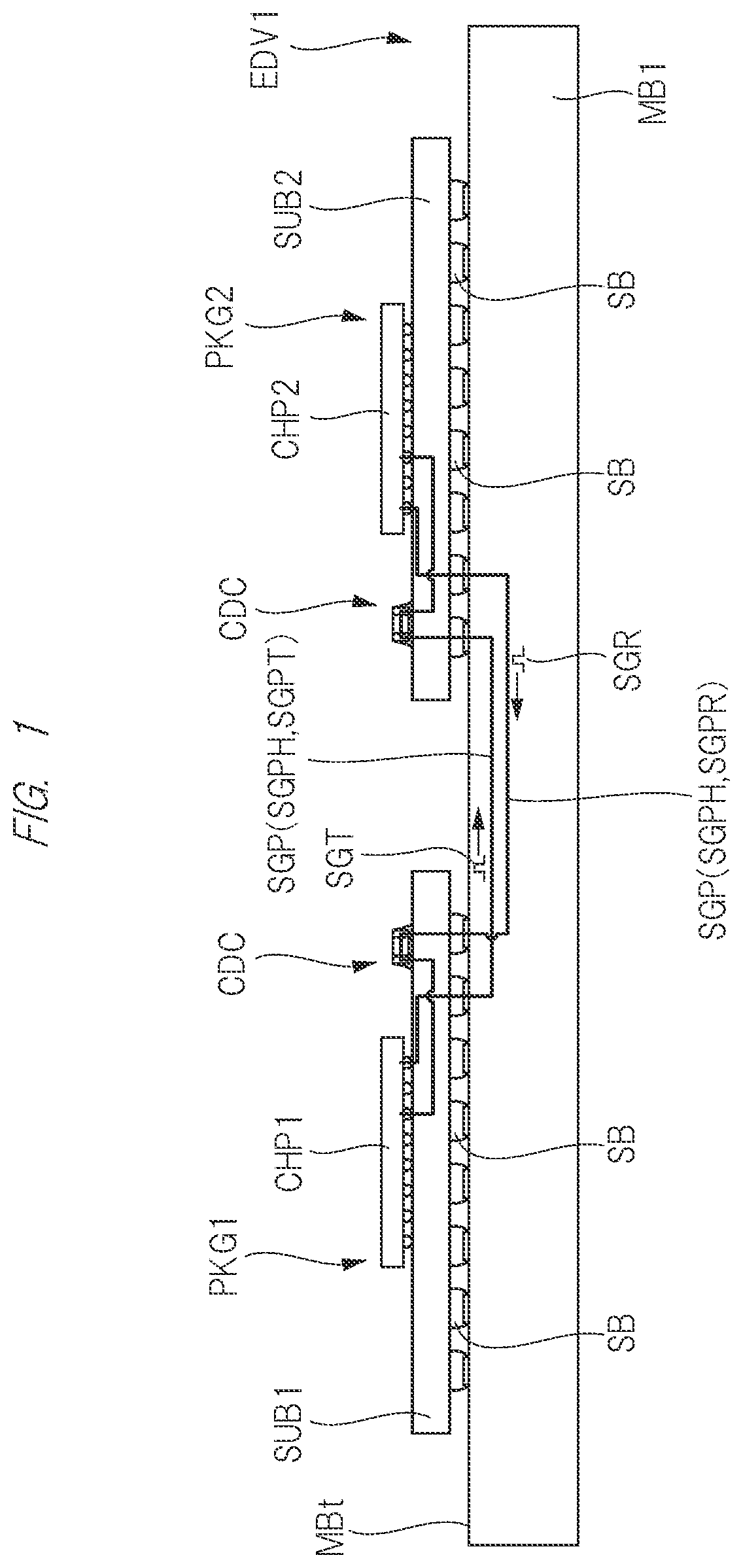
First, a configuration example of an electronic device in which a plurality of semiconductor devices (semiconductor packages) are mounted on a motherboard and electric signals are transmitted between the plurality of semiconductor devices will be described with reference to .
is an explanatory diagram showing a configuration example of an electronic device including the semiconductor device of the present embodiment.
is an explanatory diagram showing a configuration example of a circuit included in the electronic device shown in .
In , in order to explicitly indicate that the semiconductor device PKG 1 and the semiconductor device PKG 2 are electrically connected, the high-speed transmission path SGPH shown in is schematically shown by a thick line.
The electronic device (electronic device) EDV 1 shown in includes a wiring board (motherboard, mounting board) MB 1 , and a semiconductor device PKG 1 and a semiconductor device PKG 2 mounted on the wiring board MB 1 .
The semiconductor device PKG 1 and the semiconductor device PKG 2 are electrically connected to each other via a signal transmission path SGP formed in the wiring board MB 1 .
The signal transmitted through the signal transmission path SGP includes a signal SGT outputted from the semiconductor device PKG 1 and a signal SGR inputted to the semiconductor device PKG 1 .
The signal transmission path SGP includes a signal transmission path SGPT through which the signal SGT is transmitted and a signal transmission path SGPR through which the signal SGR is transmitted.
In the embodiment shown in , the signal SGT is outputted from the semiconductor device PKG 1 , and the signal SGT is inputted to the semiconductor device PKG 2 .
The signal SGR is outputted from the semiconductor device PKG 2 , and the signal SGR is inputted to the semiconductor device PKG 1 .
However, the output destination of the signal SGT and the output source of the signal SGR are not limited to the example shown in , and there are various modified examples.
Since the semiconductor device PKG 1 and the semiconductor device PKG 2 shown in have the same structures, the semiconductor device PKG 1 will be representatively described below.
As shown in , the electronic device EDV 1 has a plurality of signaling paths SGPs.
In the examples shown in , the plurality of signal transmission paths SGPs connected to the semiconductor device PKG 1 include a low-speed transmission path (low-speed signal transmission path) SGPL through which an electric signal is transmitted at a first transmission rate, and a high-speed transmission path (high-speed signal transmission path) SGPH through which an electric signal is transmitted at a second transmission rate higher than the first transmission rate.
In the embodiment shown in , the high-speed transmission path SGPH includes a pair of differential signal transmission paths DSp and DSn through which differential signals are transmitted.
In the present embodiment, an embodiment in which a differential signal is transmitted through a pair of differential signal transmission paths DSp and DSn is described as an example of the high-speed transmission path SGPH, but various modifications other than the differential signal can be applied to the type of the high-speed signal.
For example, even in the case of a so-called single-ended structure in which one signal transmission path SGP is used, high-speed transmission can be performed by increasing the frequency.
As shown in , the semiconductor chip CHP 1 of the semiconductor device PKG 1 includes a plurality of electrodes.
The plurality of electrodes of the semiconductor chip CHP 1 include signal electrodes Tx (specifically, signal electrodes Txp and Txn for outputting a pair of differential signals) through which a signal SGT (see ) as an output signal (transmission signal) is transmitted.
The plurality of electrodes of the semiconductor chip CHP 1 include signal electrodes Rx (specifically, signal electrodes Rxp and Rxn to which a pair of differential signals are input) to which a signal SGR (see ) as an input signal (reception signal) is transmitted.
In addition, in the embodiment shown in , the plurality of electrodes of the semiconductor chip CHP 1 includes a signal electrode (low-speed signal electrode) TxL and a signal electrode (low-speed signal electrode) RxL, which are connected to the low-speed transmission path SGPL.
The plurality of electrodes of the semiconductor chip CHP 1 include a power supply potential electrode Vd to which the power supply potential VDD is supplied and a reference potential electrode Vs to which the reference potential VSS is supplied.
The power supply potential VDD is supplied to the semiconductor chip CHP 1 (i.e., circuits included in the semiconductor chip CHP 1 ) via the power supply potential electrodes Vd.
The reference potential VSS is supplied to the semiconductor chip CHP 1 via the reference potential electrodes Vs.
At least a part of the plurality of circuits included in the semiconductor chip CHP 1 is driven by a driving voltage generated by a potential difference between the power supply potential VDD and the reference potential VSS.
The reference potential VSS is, for example, a ground potential, and the power supply potential VDD is higher than the reference potential VSS.
The electronic device EDV 1 has a capacitor CPS for a power supply circuit that is inserted into the power supply circuit in parallel.
The capacitor CPS shown in is inserted between a reference potential supply path VSP for supplying the reference potential VSS to the semiconductor chip CHP 1 and a power supply potential supply path VDP for supplying the power supply potential VDD to the semiconductor chip CHP 1 .
The capacitor CPS can function as a bypass capacitor that bypasses and flows noise (signal) included in the power supply potential supply path VDP to the reference potential supply path VSP side.
In addition, the capacitor CPS can function as a decoupling capacitor that reduces the effect of the impedance components included in the power supply potential supply path VDP and the reference potential supply path VSP by reducing the loop (path length) of the current flowing through the circuits formed on the CHP 1 of the semiconductor chip, thereby reducing the influence of the impedance components included in the power supply potential supply path VDP and the reference potential supply path VSP.
In addition, by connecting the capacitor CPS to the vicinity of the circuit which consumes the supplied power, it is possible to function as a battery which suppresses a phenomenon that the driving voltage drops instantaneously.
The bypass capacitor, the decoupling capacitor, or the capacitor CPS for the power supply circuit used as the battery are all inserted in the power supply circuit in parallel connection.
On the other hand, the capacitor CDC is inserted in the signal transmission path SGP in series connection.
Therefore, as shown in , when the high-speed transmission path SGPH is configured by the differential signal transmission paths DSp and DSn, the capacitors CDC are inserted into the differential signal transmission path DSp and the differential signal transmission path DSn, respectively.
When signals are transmitted at high speed as in the electronic device EDV 1 , it is preferable to connect the capacitor CDCs in series during the high-speed transmission path SGPH.
The DC components included in the AC signals can be cut off by the capacitor CDC inserted in the high-speed transmission path SGPH.
This makes it possible to stabilize the input and output of signals at high speed.
The capacitor CDC, which is inserted in the signal transmission path in series and cuts the DC components in the AC signal, is called a DC (Direct Current) cutting capacitor or an AC (Alternate Current) coupling capacitor (hereinafter referred to as a DC cutting capacitor).
In the low-speed transmission path SGPL shown in , electric signals are transmitted at a transmission rate of, for example, less than 3 Gbps(Gigabit per second).
In the high-speed transmission path SGPH formed by electrically connecting the signal electrode Tx and the signal electrode Rx, an electric signal is transmitted at a transmission rate of, for example, about 10 Gbps to 60 Gbps.
is a top view of one of the two semiconductor devices shown in , is cross-sectional view of a wiring substrate constituting the semiconductor device shown in , is a bottom view of the semiconductor device shown in , and is plan view of an electrode arrangement surface of the semiconductor chip shown in .
is cross-sectional view of a main part along line X 1 -X 1 ′ of , and is cross-sectional view of a main part along line X 2 -X 2 ′ of .
However, since the cross-sectional views along the line X 1 -X 1 ′ and the line X 2 -X 2 ′ in are symmetrical with respect to the center line of the semiconductor device in the X direction, the right half region is shown in , for example.
is cross-sectional view of a main part along line Y 1 -Y 1 ′ of .
However, since the cross-sectional view along the line Y 1 -Y 1 ′ in is symmetrical with respect to the center line of the semiconductor device in the Y direction, shows, for example, an upper half region.
is plan view of wiring connecting electrodes of a semiconductor chip and solder balls on a wiring substrate, and
is plan view of wiring connecting electrodes of a semiconductor chip and solder balls on a wiring substrate, which is a comparative example.
As shown in , the semiconductor device PKG 1 includes a rectangular wiring substrate SUB 1 , a rectangular semiconductor chip CHP 1 , a plurality of capacitors CPS and CDC, and a substantially rectangular lid LD.
The wiring substrate SUB 1 and the lid LD have substantially the same size and are larger than the size of the semiconductor chip CHP 1 .
The wiring substrate SUB 1 having a rectangular shape in plan view has an upper surface 2 t, and the upper surface 2 t includes two sides 2 X extending in the X direction and two sides 2 Y extending in the Y direction perpendicular to the X direction. The semiconductor chip CHP 1 is mounted on the center portion of the upper surface 2 t of the wiring substrate SUB 1 .
The quadrangular semiconductor chip CHP 1 in plan view includes two sides 3 X extending in the X direction and two sides 3 Y extending in the Y direction.
An underfill resin UF is provided so that the underfill resin UF contacts the semiconductor chip CHP 1 and surrounds the periphery of the semiconductor chip CHP 1 .
A plurality of capacitors CDCs and CPSs are mounted on the upper surface 2 t of the wiring substrate SUB 1 .
The plurality of capacitors CDC and CPS are capacitor components called chip capacitors having two terminals at both ends of a rectangular parallelepiped.
A plurality of capacitors CDCs are arranged between the semiconductor chip CHP 1 and one side 2 Y extending in the Y-direction.
The plurality of capacitors CDCs are disposed closer to one side 2 Y than the semiconductor chip CHP 1 .
The plurality of capacitors CDC are arranged in a matrix, e.g., two rows in the X direction and nine columns in the Y direction, for a total of eighteen capacitors CDC.
In the two capacitors CDC arranged in the X direction, the two terminals of each capacitor CDC are aligned in the X direction.
That is, the four terminals of the two capacitors CDC arranged in the X direction are aligned in the X direction.
In other words, in plan view, the long side of the rectangular capacitor CDC is arranged along the X direction, and the short side thereof is arranged along the Y direction.
Similarly, between the semiconductor chip CHP 1 and the other side 2 Y extending in the Y direction, a plurality of capacitors CDC are arranged in a matrix-like manner, for example, two rows in the X direction and nine columns in the Y direction, and a total of eighteen capacitors CDC are arranged between the semiconductor chip CHP 1 and the other side 2 Y extending in the Y direction.
For example, a plurality of capacitors CDC arranged between the semiconductor chip CHP 1 and one side 2 Y extending in the Y direction are connected to the high-speed transmission path SGPH for the signal transmission rate 56 Gbps, and a plurality of capacitors CDC arranged between the semiconductor chip CHP 1 and the other side 2 Y extending in the Y direction are connected to the high-speed transmission path SGPH for the signal transmission rate 25 Gbps.
Between the semiconductor chip CHP 1 and one side 2 X extending in the X direction, a plurality of capacitors CPS are arranged in a row along the X direction.
The plurality of capacitors CPSs are disposed closer to the semiconductor chip CHP 1 than one side 2 X.
A total of five capacitors CPS are arranged at predetermined intervals in the X direction.
The two terminals of each capacitor CPS are aligned in the Y direction.
In other words, in plan view, the long side of the rectangular capacitor CPS is arranged along the Y direction, and the short side thereof is arranged along the X direction.
Similarly, a plurality of capacitors CPS are arranged in a line along the X direction between the semiconductor chip CHP 1 and the other side 2 X extending in the X direction.
As shown in , the upper surfaces 2 t of the semiconductor chip CHP 1 and the wiring substrate SUB 1 are covered with a lid LD.
The quadrangular lid LD in plan view includes two sides 4 X extending in the X direction and two sides 4 Y extending in the Y direction.
Since the lid LD is chamfered at the intersection of the side 4 X and the side 4 Y, the semiconductor chip CHP 1 can be said to be substantially rectangular in plan view.
The lid LD includes a heat radiating portion 4 a, a flange portion 4 b surrounding the periphery of the heat radiating portion 4 a, and an inclined portion 4 s between the heat radiating portion 4 a and the flange portion 4 b.
The radiator 4 a includes an opening portion 4 e for exposing a plurality of capacitors CPS arranged between the semiconductor chip CHP 1 and one side 2 X, and an opening portion 4 e for exposing a plurality of capacitors CPS arranged between the semiconductor chip CHP 1 and the other side 2 X.
In plan view, the two opening portions 4 e are located on the outer side of the semiconductor chip CHP 1 without overlapping with the semiconductor chip CHP 1 .
The flanged portion 4 b has a notch portion 4 d 1 exposing a plurality of capacitors CDC arranged between the semiconductor chip CHP 1 and one side 2 Y on a part of one side 4 Y, and has a notch portion 4 d 1 exposing a plurality of capacitors CDC arranged between the semiconductor chip CHP 1 and the other side 2 Y on a part of the other side 4 Y.
Further, the flange portion 4 b is provided with two notches 4 d 2 on each of the sides 4 X extending in the X direction.
The notched portion 4 d 1 is a concave portion from the side 4 Y toward the heat radiating portion 4 a, and the notched portion 4 d 2 is a concave portion from the side 4 X toward the heat radiating portion 4 a.
Further, the flanges 4 b are provided with four corner portions 4 c, and at the corner portions 4 c, the lid LDs are bonded to the wiring substrate SUB 1 via adhesive layers.
The corner portion 4 c is defined as a region sandwiched between the notch portion 4 d 1 and the notch portion 4 d 2 in the flange portion 4 b.
That is, as shown in , the corner portion 4 c is provided with an adhesive layer region ADR 2 which is a coating region of an insulating adhesive layer.
Further, between the two notches 4 d 2 in the X-direction, an adhesive layer region ADR 1 , which is a coating region of a conductive adhesive layer, is provided.
In other words, the flange part 4 b of the riddle LD has an adhesive area ADR 1 or ADR 2 almost all the circumference except for the missing part 4 d 1 and 4 d 2 .
As shown in , the wiring substrate SUB 1 has an upper surface (surface, main surface, chip mounting surface, first main surface) 2 t on which the semiconductor chip CHP 1 is mounted, and a lower surface (surface, main surface, mounting surface, second main surface) 2 b which is opposed to the upper surface 2 t.
The wiring substrate SUB 1 is an interposer (relay board) that electrically connects the semiconductor chip CHP 1 mounted on the upper surface 2 t and the wiring board MB 1 (see ) that is a motherboard (mounting board) to each other.
The wiring substrate SUB 1 has a plurality of wiring layers WL 1 , WL 2 , WL 3 , WL 4 , WL 5 , WL 6 , WL 7 , WL 8 , WL 9 , and WL 10 (10 layers in the embodiment shown in ) for electrically connecting the terminal on the upper surface 2 t side, which is the chip-mounting surface, and the terminal on the lower surface 2 b side, which is the chip-mounting surface.
Each wiring layer has a conductor pattern such as a wiring which is a path for supplying an electric signal or electric power.
An insulating layer 2 e is disposed between the wiring layers. Each wiring layer is electrically connected via a via 2 v, which is an interlayer conductive path penetrating the insulating layer 2 e, or through-hole wiring 2 THW.
In addition, most of the wiring layer WL 1 disposed on the uppermost surface 2 t side of the plurality of wiring layers is covered with the insulating layer SR 1 which is a solder resist film.
In addition, most of the wiring layer WL 10 disposed on the lowermost surface 2 b of the plurality of wiring layers is covered with the insulating layer SR 2 which is a solder resist film.
The wiring substrate SUB 1 is formed, for example, by laminating a plurality of wiring layers on the upper surface 2 Ct and the lower surface 2 Cb of an insulating layer (core material, core insulating layer) 2 CR made of glass cloth by a build-up method.
The wiring layer WL 5 on the upper surface 2 Ct side of the insulating layer 2 CR and the wiring layer WL 6 on the lower surface 2 Cb side are electrically connected via a plurality of through-hole wirings 2 THW embedded in a plurality of through-holes provided so as to pass through one of the upper surface 2 Ct and the lower surface 2 Cb to the other.
A plurality of pads (terminals, bonding pads, bonding leads, and semiconductor chip connecting terminals) 2 PD electrically connected to the semiconductor chip CHP 1 are formed on the upper surface 2 t of the wiring substrate SUB 1 .
On the lower surface 2 b of the wiring substrate SUB 1 , a plurality of lands 2 LD, which are external input/output terminals of the semiconductor device PKG 1 , are formed.
The plurality of pads 2 PD and the plurality of lands 2 LD are electrically connected to each other via wirings 2 d, vias 2 v, and through-hole wirings 2 THW formed on the wiring substrate SUB 1 .
In the examples shown in , the wiring substrate SUB 1 shows a wiring board in which a plurality of wiring layers are stacked on the upper surface 2 Ct side and the lower surface 2 Cb side of the insulating layer 2 CR, which is a core material.
However, as a modification to , a so-called coreless substrate may be used in which the insulating layer 2 CR made of a hard material such as a core material is not provided, and conductor patterns such as the insulating layer 2 e and the wiring 2 d are formed by stacking in order.
When the coreless substrate is used, the through-hole wiring 2 THW is not formed, and each wiring layer is electrically connected via the via 2 v.
Although exemplarily shows a wiring substrate SUB 1 having 10 wiring layers, a wiring board having 11 or more wiring layers or 8 or less wiring layers may be used as a modification, for example.
In the example shown in , solder balls (solder material, external terminals, electrodes, and external electrodes) SB are connected to each of the plurality of lands 2 LD.
The solder balls SB are conductive members that electrically connect the plurality of terminals (not shown) on the wiring board MB 1 and the plurality of lands 2 LD when the semiconductor device PKG 1 is mounted on the wiring board MB 1 shown in .
The solder ball SB is, for example, an Sn—Pb solder material containing lead (Pb), or a solder material made of a so-called lead-free solder that does not substantially contain Pb.
Examples of lead-free solder include, for example, tin (Sn), tin-bismuth (Sn—Bi), tin-copper-silver (Sn—Cu—Ag), tin-copper (Sn—Cu), and the like.
Here, the lead-free solder means a solder in which the content of lead (Pb) is 0.1 wt % or less, and this content is determined as a standard of the RoHS (Restriction of Hazardous Substances) command.
As shown in , the plurality of solder balls SB are arranged in a matrix.
Although not shown in , a plurality of lands 2 LD (see ) to which a plurality of solder balls SB are bonded are also arranged in a matrix form.
In this manner, a semiconductor device in which a plurality of external terminals (solder balls SB and lands 2 LD) are arranged in a matrix on the mounting surface of the wiring substrate SUB 1 is referred to as an area-array type semiconductor device.
The area array-type semiconductor device can effectively utilize the mounting surface (lower surface 2 b ) of the wiring substrate SUB 1 as a space for arranging external terminals, which is preferable in that an increase in the mounting area of the semiconductor device can be suppressed even if the number of external terminals increases.
In other words, a semiconductor device in which the number of external terminals increases with higher functionality and higher integration can be mounted in a space-saving manner.
The semiconductor device PKG 1 includes a semiconductor chip CHP 1 mounted on the wiring substrate SUB 1 .
As shown in , the semiconductor chip CHP 1 includes a front surface (main surface, upper surface) 3 t and a back surface (main surface, lower surface) 3 b which is opposed to the front surface 3 t.
As shown in , the semiconductor chip CHP 1 has a rectangular outer shape having a plane area smaller than that of the wiring substrate SUB 1 in plan view.
In the embodiment shown in , the semiconductor chip CHP 1 is mounted on the central portion of the upper surface 2 t of the wiring substrate SUB 1 , and each of the four sides 3 X and 3 Y of the semiconductor chip CHP 1 extends along each of the four sides 2 X and 2 Y of the wiring substrate SUB 1 .
As shown in , a plurality of electrodes (pads, electrode pads, bonding pads) 3 PD are arranged in a matrix on the front surface 3 t of the semiconductor chip CHP 1 .
In addition, in the embodiment shown in , the semiconductor chip CHP 1 is mounted on the wiring substrate SUB 1 with the front surface 3 t facing the upper surface 2 t of the wiring substrate SUB 1 .
Such a mounting method is called a face-down mounting method or a flip-chip connection method.
Although not shown, a plurality of semiconductor elements (circuit elements) are formed on the main surface of the semiconductor chip CHP 1 (more specifically, a semiconductor element forming area provided on an element forming surface of a semiconductor substrate which is a base material of the semiconductor chip CHP 1 ).
The plurality of electrodes 3 PD are electrically connected to the plurality of semiconductor elements via wirings (not shown) formed in wiring layers disposed inside the semiconductor chips CHP 1 (in detail, between the front surfaces 3 t and semiconductor element forming regions (not shown)).
The semiconductor chip CHP 1 (more specifically, the base material of the semiconductor chip CHP 1 ) is made of, for example, silicon (Si).
An interlayer insulating film covering the base material and the wirings of the semiconductor chip CHP 1 is formed on the front surface 3 t, and a part of each of the plurality of electrodes 3 PD is exposed from the interlayer insulating film in an opening portion formed in the interlayer insulating film.
Here, the wiring or the wiring layer is made of, for example, a metal film of copper (Cu) or the like, and the interlayer insulating film for insulating the plurality of wiring layers is made of a Low-k film or the like.
Each of the plurality of electrodes 3 PD is made of a metal film, and in the present embodiment, is made of aluminum (Al), for example.
In addition, as shown in , the plurality of electrodes 3 PD are respectively connected to the protrusion electrodes 3 BP, and the plurality of electrodes 3 PD of the semiconductor chip CHP 1 and the plurality of pads 2 PD of the wiring substrate SUB 1 are electrically connected to each other via the plurality of protrusion electrodes 3 BP.
The protruding electrodes (bump electrodes) 3 BP are metallic members (conductive members) formed so as to protrude above the surfaces 3 t of the semiconductor chips CHP 1 .
In the present embodiment, the protruding electrode 3 BP is a so-called solder bump in which a solder material is laminated on the electrode 3 PD via an under-bump metal film.
As the base metal film, for example, a laminated film in which titanium (Ti), copper (Cu), and nickel (Ni) are laminated from the connection surface side with the electrode 3 PD (in some cases, a gold (Au) film is further formed on the nickel film) can be exemplified.
As a solder material constituting the solder bump, a solder material containing lead or a lead-free solder can be used, similarly to the above-described solder ball SB.
When the semiconductor chip CHP 1 is mounted on the wiring substrate SUB 1 , solder bumps are formed in advance on both of the plurality of electrodes 3 PD and the plurality of pads 2 PD, and the solder bumps are contacted with each other by performing a heat treatment (reflow treatment), whereby the solder bumps are integrated to form the protruding electrodes 3 BP.
As a modification to the present embodiment, a pillar bump (columnar electrode) in which a solder film is formed on the tip surface of a conductor pillar made of copper (Cu) or nickel (Ni) may be used as the projection electrode 3 BP.
As shown in , an underfill resin UF is disposed between the semiconductor chip CHP 1 and the wiring substrate SUB 1 . The underfill resin UF is disposed so that the underfill resin UF closes a space between the surface 3 t of the semiconductor chip CHP 1 and the upper surface 2 t of the wiring substrate SUB 1 .
The underfill resin UF is made of an insulating (non-conductive) material (e.g., a resin material), and is disposed so as to seal the electrical connecting portions (the bonding portions of the plurality of protruding electrodes 3 BP) of the semiconductor chip CHP 1 and the wiring substrate SUB 1 .
In this manner, by covering the bonding portions between the plurality of protrusion electrodes 3 BP and the plurality of pads 2 PD with the underfill resin UF, it is possible to alleviate the stresses generated in the electrically connecting portions between the semiconductor chips CHP 1 and the wiring substrate SUB 1 .
That is, it is possible to alleviate the stress generated in the bonding portion between the plurality of electrodes 3 PD and the plurality of protruding electrodes 3 BP of the semiconductor chip CHP 1 and the stress generated in the bonding portion between the plurality of protruding electrodes 3 BP and the plurality of pads 2 PD of the wiring substrate SUB 1 .
Furthermore, the main surface of the semiconductor chips CHP 1 on which the semiconductor elements are formed can be protected.
In addition, in the embodiment shown in , a lid (heat sink) LD is attached to the back surface 3 b of the semiconductor chip CHP 1 .
The lid LD is, for example, a metallic plate having a thermal conductivity higher than that of the wiring substrate SUB 1 , and the lid LD has a function of discharging heat generated in the CHP 1 of the semiconductor chip to the outside.
The lid LD is made of, for example, a metal material such as copper (Cu) or aluminum (Al), and can have a thickness of 0.3 to 3.0 mm, and in the present embodiment, the thickness is, for example, 1 mm.
The lid LD is attached to the back surface 3 b of the semiconductor chip CHP 1 via the adhesive layer AD 3 .
Adhesive AD 3 , for example, has a higher thermal conductivity than underfill resin UF by containing, for example, a large number of metal particles and fillers (e.g., alumina).
As shown in , the semiconductor chip CHP 1 is bonded to the heat radiating portion 4 a of the lid LD.
The heat radiating portion 4 a has a convex shape with respect to the flange portion 4 b, and the height HLa of the heat radiating portion 4 a is higher than the height HLb of the flange portion 4 b (Hla>HLb).
Here, the height HLa of the heat radiating portion 4 a is a distance from the upper surface 2 t of the wiring substrate SUB 1 to the back surface LDb of the heat radiating portion 4 a, and the height HLb of the flange portion 4 b is a distance from the upper surface 2 t of the wiring substrate SUB 1 to the back surface LDb of the flange portion 4 b.
As shown in , the lid LD has a notch 4 d 1 in the flange 4 b, and two capacitors CDC (p 1 ) and CDC (n 1 ) are mounted on the upper surface 2 t of the wiring substrate SUB 1 exposed from the lid LD in the notch 4 d 1 .
Each capacitor CDC has terminals C 1 and C 2 at both longitudinal ends thereof, and each of the terminals C 1 and C 2 is connected to an electrode 2 f of the wiring substrate SUB 1 by a bonding material 2 g such as solder.
That is, the electrode 2 f to which the terminal C 1 of the capacitor CDC(p 1 ) is connected is electrically connected to the pad 2 PD(Rxp 1 ) via the wiring 2 d (p 1 ) in the wiring substrate SUB 1 , and is electrically connected to the electrode 3 PD(Rxp 1 ) of the semiconductor chip CHP 1 via the projection electrode 3 BP.
The electrodes 2 f to which the terminals C 2 of the capacitors CDC(p 1 ) are connected are electrically connected to the lands 2 LD and the solder balls SB(Rxp 1 ) via the wirings 2 d ′(p 1 ) in the wiring substrate SUB 1 .
The capacitor CDC(p 1 ) is connected in series between the electrodes 3 PD(Rxp 1 ) of the semiconductor chip CHP 1 and the corresponding solder balls SB(Rxp 1 ).
Here, the wiring 2 d ′(p 1 ) includes the wiring 2 d, the via 2 v, and the through-hole wiring 2 THW in the wiring substrate SUB 1 .
In , a wire 2 d ′(n 1 ) indicated by a broken line indicates the connections between the electrodes 3 PD(Rxn 1 ) of the semiconductor chip CHP 1 and the solder balls SB(Rxn 1 ) arranged in the back of the semiconductor chip Rxn 1 .
corresponds to the first pair of differential signal transmission paths DSp 1 and DSn 1 shown in , which will be described later.
In the present embodiment, since the thickness T 1 of the semiconductor chip CHP 1 is made thinner than the thickness T 2 of the capacitor CDC, the height HC of the capacitor CDC becomes higher than the height HLa of the heat radiating portion 4 a, and it becomes difficult to accommodate the capacitor CDC in the space between the lid LD and the wiring substrate SUB 1 .
However, by arranging the plurality of capacitors CDC in the notched portion 4 d 1 of the lid LD, the capacitor CDC can be mounted on the upper surface 2 t of the wiring substrate SUB 1 without short-circuiting between the terminals C 1 and C 2 of the capacitor CDC by the lid LD.
As described with reference to , the capacitor CDC is connected in series in the high-speed transmission path SGPH, and the capacitor CDC has a function of cutting DC components included in the AC signal in the input signal input to the semiconductor chip CHP 1 via the solder ball SB.
By mounting the capacitor CDCs on the wiring substrate SUB 1 , noises in inputted signals can be reduced.
This is because, if the capacitor CDC is formed on the circuit board MB instead of the semiconductor device PKG 1 , there is a high possibility that the input signal will be noisy between the capacitor CDC and the semiconductor device PKG 1 .
Here, the capacitor CDC indicates both the capacitor CDC(p 1 ) and the capacitor CDC(n 1 ) shown in .
Further, as shown in , the capacitor CDC is arranged in the peripheral portion (or end portion) of the wiring substrate SUB 1 by providing the notch portion 4 d 1 on the side 4 Y of the lid LD and arranging the capacitor CDC in the notch portion 4 d 1 .
The capacitors CDCs are disposed closer to the side 2 Y than the semiconductor chip CHP 1 .
For example, it is conceivable to provide an opening portion in the lid LD and arrange the capacitor CDC in the opening portion, but arranging the capacitor CDC in the notched portion 4 d 1 of the side 4 Y enables the capacitor CDC to be arranged more in the peripheral portion of the wiring substrate SUB 1 .
By arranging the capacitor CDCs in the peripheral portion of the wiring substrate SUB 1 , the degree of freedom in laying out the wiring 2 d on the wiring substrate SUB 1 is improved, and accordingly, the electric performance of the semiconductor device PKG 1 is also improved.
This is because the wiring 2 d in the wiring substrate SUB 1 extends radially from the central portion in which the semiconductor chip CHP 1 is mounted to the peripheral portion, so that the wiring density is higher in the central portion, and the wiring density is lower in the central portion to the peripheral portion.
As shown in , the capacitor CPS is mounted on the wiring substrate SUB 1 so that the capacitor CPS is exposed from the opening portion 4 e provided in the heat radiating portion 4 a of the lid LD.
Similar to the capacitor CDC, the height HC of the capacitor CPS is higher than the height HLa of the radiator 4 a, but by arranging the capacitor CPS in the opening portion 4 e of the lid LD, the capacitor CPS can be mounted on the upper surface 2 t of the wiring substrate SUB 1 without short-circuiting between the terminals C 1 and C 2 of the capacitor CPS due to the lid LD.
As shown in , the electrode 2 f to which the terminal C 1 is connected is electrically connected to the power supply potential pad 2 PD(Vd) via the wiring 2 d ′ in the wiring substrate SUB 1 , is electrically connected to the power supply potential electrode 3 PD(Vd) of the semiconductor chip CHP 1 via the projection electrode 3 BP, and is further connected to the power supply potential land LVd and the solder ball SB via the wiring 2 d ′.
The electrode 2 f to which the terminal C 2 is connected is electrically connected to the pads 2 PD for the reference potential via the wiring 2 d ′ in the wiring substrate SUB 1 , is electrically connected to the electrodes 3 PD for the reference potential of the semiconductor chip CHP 1 via the protruding electrodes 3 BP, and is further connected to the lands LVs for the reference potential and the solder balls SB via the wiring 2 d′.
As described with reference to , the capacitor CPS is disposed closer to the semiconductor chip CHP 1 than the one side 2 X.
By arranging the capacitor CPS close to the semiconductor chip CHP 1 , the driving voltage, which is the difference between the power supply potential VDD of the semiconductor chip CHP 1 and the reference voltage VSS, can be stabilized.
As shown in , the flanges 4 b of the lid LDs are connected to the electrodes 2 f provided on the wiring substrate SUB 1 via conductive adhesive layers AD 1 .
The electrode 2 f to which the lid LD is connected is connected to a solder ball SB to which a reference potential VSS is applied via a wiring 2 d′.
By applying the reference potential VSS to the lid LD, the semiconductor chip CHP 1 can be shielded, and the semiconductor chip CHP 1 can be protected from a magnetic field or the like generated outside the semiconductor device PKG 1 .
Further, as shown in , in plan view, the rectangular capacitor CPS is arranged with its long side along the Y direction and its short side along the X direction.
In other words, the long side of the capacitor CPS extends in the Y direction perpendicular to the X direction, which is the extending direction of the side 3 X of the semiconductor chip CHP 1 sandwiching the capacitor CPS and the side 2 X of the wiring substrate SUB 1 .
With such an arrangement, the degree of freedom in laying out the wiring 2 d on the wiring substrate SUB 1 can be improved.
In the case of the present embodiment, the two electrodes 2 f to which the two terminals C 1 and C 2 of the capacitor CPS are connected can be arranged side by side along the extending direction (Y direction) of the wiring 2 d.
However, when the long side of the capacitor CPS is arranged along the X direction, the two electrodes 2 f to which the two terminals C 1 and C 2 of the capacitor CPS are connected must be arranged side by side in the X direction.
is cross-sectional view of a main part along line X 2 -X 2 ′ of .
In , however, the adhesive layer regions ADR 1 and ADR 2 , which are application regions of the adhesive layer, are shown, while in , the lid LD is shown bonded to the upper surface 2 t of the wiring substrate SUB 1 .
As shown in , the adhesive layers AD 1 and AD 2 extend over the entire flange portion 4 b of the lid LD.
However, as shown in , by providing the notch 4 d 2 on the side 4 X of the lid LD, it is possible to prevent the insulating (non-conductive) adhesive layer AD 2 and the conductive adhesive layer AD 1 from contacting or mixing with each other.
Therefore, it is possible to prevent the adhesive strength of the adhesive layers AD 1 and AD 2 from decreasing.
The adhesive layer AD 1 is made of, for example, epoxy resin or solder material containing a large number of metal particles such as silver, and the adhesive layer AD 2 is made of, for example, epoxy resin.
is plan view for explaining connections from the lands LDH of the semiconductor device PKG 1 to the signal electrodes Rx of the semiconductor chips CHP 1 in the high-speed transmission path SGPH shown in .
The signal SGR, which is an input signal shown in , is input to the land LDH of the semiconductor device PKG 1 shown in , and is input to the signal electrodes Rx of the semiconductor chips CHP 1 via the capacitor CDC.
In , the land LDH in corresponds to the solder ball SB, and the signal electrode Rx in corresponds to the electrode 3 PD.
is a comparative example of , in which the direction of the capacitor CDC is different.
In , three pairs of high-speed transmission paths are shown, and each high-speed transmission path is composed of a pair of differential signal transmission paths DSp and DSn.
The first pair of differential signal transmission paths DSp 1 and DSn 1 and the constituent elements thereof are distinguished by attaching 1 to the end of the code, the second pair of differential signal transmission paths DSp 2 and DSn 2 and the constituent elements thereof are attached by attaching 2 to the end of the code, and the third pair of differential signal transmission paths DSp 3 and DSn 3 and the constituent elements thereof are attached by attaching 3 to the end of the code.
However, in the case where the first to third symbols are not distinguished from each other, 1 to 3 at the end of the code are excluded from the description.
The differential signal transmission path DSp 1 of the first pair of differential signal transmission paths DSp 1 and DSn 1 is composed of solder balls SB(Rxp 1 )/wiring 2 d ′(p 1 )/capacitor CDC(p 1 )/wiring 2 d ′(p 1 )/electrode 3 PD(Rxp 1 ), and the differential signal transmission path DSn 1 is composed of solder balls SB(Rxn 1 )/wiring 2 d ′(n 1 )/capacitor CDC(n 1 )/wiring 2 d ′(n 1 )/electrode 3 PD(Rxn 1 ).
Similarly, the differential signal transmission path DSp 2 of the second pair of differential signal transmission paths DSp 2 and DSn 2 is composed of the solder ball SB(Rxp 2 )/wiring 2 d ′(p 2 )/capacitor CDC(p 2 )/wiring 2 d ′(p 2 )/electrode 3 PD(Rxp 2 ), and the differential signal transmission path DSn 2 is composed of the solder ball SB(Rxn 2 )/wiring 2 d ′(n 2 )/capacitor CDC(n 2 )/wiring 2 d ′(n 2 )/electrode 3 PD(Rxn 2 ).
Similarly, the differential signal transmission path DSp 3 of the third pair of differential signal transmission paths DSp 3 and DSn 3 is composed of the solder ball SB(Rxp 3 )/wiring 2 d ′(p 3 )/capacitor CDC(p 3 )/wiring 2 d ′(p 3 )/electrode 3 PD(Rxp 3 ), and the differential signal transmission path DSn 3 is composed of the solder ball SB(Rxn 3 )/wiring 2 d ′(n 3 )/capacitor CDC(n 3 )/wiring 2 d ′(n 3 )/electrode 3 PD(Rxn 3 ).
The wirings 2 d ′(p 1 ) and 2 d ′(n 1 ) of the first pair of differential signal transmission paths DSp 1 and DSn 1 are equal in length.
The same applies to the second pair of differential signal transmission paths DSp 2 and DSn 2 and the third pair of differential signal transmission paths DSp 3 and DSn 3 .
The pair of solder balls SB (Rxp 1 ) and SB (Rxn 1 ), SB (Rxp 2 ) and SB (Rxn 2 ), and SB (Rxp 3 ) and SB (Rxn 3 ) are arranged adjacently to each other in the Y-direction at pitches P 1 .
These solder balls are assigned to the rows of the outermost solder balls SB shown in .
The capacitor CDC is a rectangle having a length L of the long side and a width W of the short side in plan view, and has terminals C 1 and C 2 at both ends in the long side direction.
The length L of the long side is larger than the width W of the short side (L>W).
The pair of capacitors CDC(p) and CDC(n) included in the pair of differential signal transmission paths DSp and DSn are adjacent to each other in the X direction, and the long sides thereof are arranged along the X direction.
Here, the X direction is a direction perpendicular to the extending direction of the side 3 Y of the semiconductor chip CHP 1 and the side 2 Y of the wiring substrate SUB 1 that sandwich the pair of capacitors CDC(p) and CDC(n).
As described above, since the pair of capacitors CDC(p) and CDC(n) are adjacent to each other in the X direction and the short sides are arranged along the Y direction, it is possible to reduce the area for configuring the pair of differential signal transmission paths DSp and DSn in the Y direction.
Therefore, the pitch P 1 in the Y direction of the pair of solder balls SB(Rxp) and SB(Rxn) included in the pair of differential signal transmission paths DSp and DSn can be reduced, and the pitch of the solder balls SB can be narrowed.
Further, since the branch points of the wirings 2 d ′ (p) and 2 d ′ (n) of the pair of differential signal transmission paths DSp and DSn that run in parallel from the semiconductor chip CHP 1 to the capacitors CDC(p) and CDC(n) are closer to the center portion of the wiring substrate SUB 1 as compared with the case of , which will be described later, the wiring lengths of the wirings 2 d ′ (p) and 2 d ′ (n) can be reduced, and high-speed transmission of an input signal can be achieved.
On the other hand, in the comparative example shown in , since the pair of capacitors CDC(p) and CDC(n) are adjacent to each other in the X direction and the long sides thereof are arranged along the Y direction, it is understood that the region for configuring the pair of differential signal transmission paths DSp and DSn in the Y direction is enlarged as compared with .
Therefore, the pitch P 2 of the pair of solder balls SB(Rxp) and SB(Rxn) included in the pair of differential signal transmission paths DSp and DSn is also increased as compared with , which is unsuitable for narrowing the pitch of the solder balls SB.
Further, since the branch points of the wirings 2 d ′(p) and 2 d ′(n) of the pair of differential signal transmission paths DSp and DSn running in parallel from the semiconductor chip CHP 1 to the capacitors CDC(p) and CDC(n) are closer to the end portions of the wiring substrate SUB 1 than in , the wiring lengths of the wirings 2 d ′(p) and 2 d ′ (n) are increased as compared with .
The semiconductor device PKG 1 of the present embodiment has the following features.
In plan view, the lid LD has a shape and an area substantially equal to those of the wiring substrate SUB 1 , and the flange portion 4 b of the lid LD is bonded to the wiring substrate SUB 1 with the adhesive layer AD 1 or the adhesive layer AD 2 at substantially the entire periphery except for the notched portions 4 d 1 and 4 d 2 .
Since the lid LD is formed of a metallic plate having higher stiffness than the wiring substrate SUB 1 , the warpage of the wiring substrate SUB 1 can be reduced.
In addition, since the thickness of the semiconductor chip CHP 1 flip-chip connected on the wiring substrate SUB 1 is made thinner than the thickness of the capacitors CDC or CPS, even if warpage occurs on the wiring substrate SUB 1 , the thin semiconductor chip CHP 1 follows the warpage, and the stresses applied to the electrically connected portions between the semiconductor chip CHP 1 and the wiring substrate SUB 1 can be relieved.
Therefore, it is possible to prevent cracks occurring in the interlayer insulating film in the CHP 1 of the semiconductor chip from occurring.
A capacitor CDC mounted on the wiring substrate SUB 1 is connected in series to the high-speed transmission path SGPH of the signal SGR inputted from the outside of the semiconductor device PKG 1 to the semiconductor chip CHP 1 .
The capacitor CDC, which is thicker than the semiconductor chip CHP 1 , is disposed in the notch 4 d 1 provided in the lid LD, and is exposed from the lid LD.
Therefore, the capacitor CDC can be mounted on the wiring substrate SUB 1 without short-circuiting between the terminals C 1 and C 2 of the capacitor CDC by the metallic lid LD.
Since the pair of capacitors CDC(p), CDC(n) connected to the pair of differential signal transmission paths DSp, DSn are arranged adjacent to each other in the X direction so that the short sides of the capacitors CDC(p) and CDC(n) are along the Y direction, the pitch P 1 in the Y direction of the solder balls SB(Rxp) and SB(Rxn) connected to the pair of differential signal transmission paths DSp, DSn can be reduced.
In addition, the wiring length of the wirings 2 d ′ (p) and 2 d ′ (n) constituting the pair of differential signal transmission paths DSp and DSn can be reduced.
In addition, the degree of freedom in laying out the wiring 2 d on the wiring substrate SUB 1 is improved.
The capacitor CDC is disposed in the notch 4 d 1 of the lid LD, and is disposed closer to the side 2 Y of the wiring substrate SUB 1 than the side 3 Y of the semiconductor chip CHP 1 sandwiching the capacitor CDC.
By arranging the capacitor CDCs in the peripheral portion of the wiring substrate SUB 1 , the degree of freedom in laying out the wiring 2 d on the wiring substrate SUB 1 is improved, and accordingly, the electric performance of the semiconductor device PKG 1 is also improved.
The capacitor CPS connected between the power supply potential electrode Vd and the reference potential electrode Vs of the semiconductor chip CHP 1 was mounted on the wiring substrate SUB 1 , and the capacitor CPS was disposed in the opening portion 4 e provided in the lid LD.
The capacitor CPS, which is thicker than the semiconductor chip CHP 1 , is disposed in the opening portion 4 e provided in the lid LD and is exposed from the lid LD.
Therefore, the capacitor CPS can be mounted on the wiring substrate SUB 1 without short-circuiting between the terminals C 1 and C 2 of the capacitor CPS by the metallic lid LD.
The capacitor CPS is disposed in the opening portion 4 e provided in the heat radiating portion 4 a of the lid LD, and is disposed closer to the side 3 X of the semiconductor chip CHP 1 than the side 2 X of the wiring substrate SUB 1 sandwiching the capacitor CPC.
By arranging the capacitor CPS close to the semiconductor chip CHP 1 , the driving voltages of the semiconductor chip CHP 1 can be stabilized.
By arranging the long sides of the capacitors CPS so as to extend in the Y-direction, the degree of freedom in laying out the wiring 2 d on the wiring substrate SUB 1 can be improved.
This is because the wiring 2 d in the wiring substrate SUB 1 extends radially from the central portion where the semiconductor chip CHP 1 is mounted to the peripheral portion of the wiring substrate SUB 1 .
Since the lid LD is connected to the electrode 2 f of the wiring substrate SUB 1 and the reference potential VSS is applied to the electrode 2 f, the lid LD has a shielding effect of protecting the semiconductor chip CHP 1 from an external magnetic field.
is a flow chart showing the manufacturing process of the semiconductor device shown in , and are cross-sectional views during the manufacturing process of the semiconductor device shown in .
First, as shown in , the wiring substrate SUB 1 on which the semiconductor chip CHP 1 and the capacitor CDC are mounted on the upper surface 2 t is prepared.
At this stage, the underfill resin UF is filled between the semiconductor chip CHP 1 and the wiring substrate SUB 1 .
Although not shown, the capacitor CPS is also mounted on the upper surface 2 t of the wiring substrate SUB 1 .
Next, as shown in , the adhesive layer AD 3 is applied on the back surface 3 b of the semiconductor chip CHP 1 to form the adhesive layer AD 3 .
The adhesive layer AD 3 is a high thermal conductivity adhesive layer containing a large number of metal particles and fillers such as alumina, and has thermosetting properties.
The adhesive layer AD 3 is, for example, a composite heat radiating material in which alumina is mixed with an insulating resin, and in addition to the high thermal conductivity resin, grease, gel, silicone material, carbon material, and the like are also applied to the adhesive layer AD 3 .
Next, as shown in , the adhesive layers AD 2 and AD 1 are applied to the adhesive layer regions ADR 2 and ADR 1 of the wiring substrate SUB 1 to form the adhesive layers AD 2 and AD 1 .
The adhesive layer AD 2 is an insulating adhesive layer made of epoxy resin and has thermosetting properties.
The adhesive layer AD 1 is a conductive adhesive layer made of an epoxy resin containing silver particles, for example, and has thermosetting properties.
The order of formation of the adhesive layers AD 3 to AD 1 is not particularly limited.
Next, as shown in to 9 , after the lid LD is mounted on the wiring substrate SUB 1 , the adhesive layers AD 1 to AD 3 are cured by performing heat treatment at, for example, 150° C.
Here, as shown in , the adhesive layer region ADR 1 and the adhesive layer region ADR 2 are separated by a notch portion 4 d 2 provided in the lid LD.
When the lid LD is mounted after the adhesive layers AD 1 and AD 2 are applied, the adhesive layers AD 1 and AD 2 are spread due to the weight of the lid LD, but since the notch portion 4 d 2 is provided in the lid LD, the two layers do not mix with each other.
In the notched portion 4 d 2 , mixing of the adhesive layers AD 1 and AD 2 can be prevented by the surface tension of the adhesive layers AD 1 and AD 2 .
Therefore, it is possible to prevent the adverse effect of the hardening inhibition or the lowering of the adhesiveness of the adhesive layers AD 1 and AD 2 caused by the mixing.
According to the method for manufacturing a semiconductor device of this embodiment, since the adhesive layers AD 1 to AD 3 can be cured by one heat treatment, the manufacturing process can be shortened.
In addition, by providing the notch 4 d 2 in the lid LD between the adhesive layer region ADR 1 and the adhesive layer region ADR 2 , it is possible to prevent the conductive adhesive layer AD 1 provided in the adhesive layer region ADR 1 from mixing with the insulating adhesive layer AD 2 provided in the adhesive layer region ADR 2 in the step of adhering the lid LD to the wiring substrate SUB 1 , so that it is possible to improve the connection reliability between the lid LD and the wiring substrate SUB 1 .
is a top view of a semiconductor device PKG 1 a of a first modification.
As shown in or , in order to provide the lid LD with a shielding function, the lid LD was connected to the electrodes 2 f of the wiring substrate SUB 1 via a conductive adhesive layer in the adhesive layer area ADR 1 .
Variation 1 shows a structure in which the lid LD does not have a shield function.
The adhesive layer region ADR 1 in is the adhesive layer region ADR 2 , and the notch portion 4 d 2 is not provided.
is a diagram of the semiconductor PKG 1 b of a second modification.
In the second modification, the capacitor CPS is disposed in the notch portion 4 d 3 provided on the side 4 X of the lid LD.
Since the opening portion is not provided in the heat dissipation portion 4 a of the lid LD, the area of the heat dissipation portion 4 a can be increased as compared with the structure of , and the heat dissipation characteristics of the semiconductor chip CHP 1 b can be improved.
When the distance between the side 3 X of the semiconductor chip CHP 1 b sandwiching the capacitor CPS and the side 2 X of the wiring substrate SUB 1 is small, for example, when the side 3 Y of the semiconductor chip CHP 1 b is longer than the side 3 X, it is useful to arrange the capacitor CPS in the notched portion 4 d 3 of the lid LD.
This is because a relatively wide area is required between the side 3 X of the semiconductor chip CHP 1 b and the side 2 X of the wiring substrate SUB 1 when the capacitor CPS is arranged in the opening portion 4 e as in the above embodiment.
When the distance between the side 3 X of the semiconductor chip CHP 1 b sandwiching the capacitor CPS and the side 2 X of the wiring substrate SUB 1 is small, even if the capacitor CPS is disposed in the notch 4 d 3 of the lid LD, the driving voltages of the semiconductor chip CHP 1 b can be stabilized because the capacitor CPS is close to the semiconductor chip CHP 1 b.
Further, by arranging the capacitor CPS in the peripheral portion of the wiring substrate SUB 1 , the degree of freedom in laying out the wiring 2 d on the wiring substrate SUB 1 is improved, and accordingly, the electric performance of the semiconductor device PKG 1 b is also improved.
The invention made by the present inventor has been described above in detail based on the embodiment, but the present invention is not limited to the embodiment described above, and it is needless to say that various modifications can be made without departing from the gist thereof.
Part of the contents described in the above embodiments will be described below.
APPENDIX 1
A method of manufacturing a semiconductor device comprising the steps of: (a) providing a wiring substrate including a first region on which a semiconductor chip is mounted, a second region in which an electrode is exposed, and a third region covered with an insulating layer on a back surface of the semiconductor chip in the first region; (b) forming a first adhesive layer on a back surface of the semiconductor chip in the second region, forming a conductive second adhesive layer on the electrode, and forming an insulating third adhesive layer on the insulating layer in the third region; (c) mounting a metallic lid comprising a notch on a main surface of the wiring substrate; (d) heat treating the first adhesive layer, the second adhesive layer, and the third adhesive layer to cure the first adhesive layer, the second adhesive layer, and the third adhesive layer; and (c) positioning the notch between the second region and the third region in the step.
Figures (16)
Citations
This patent cites (7)
- US6239486
- US10056323
- US20040166763
- US20170033038
- US20180158772
- US2000-311960
- US2015/162768