Abstract
A semiconductor device includes: an insulating substrate; a first semiconductor element connected to the insulating substrate; a conductive member disposed on the insulating substrate, and including a first opposing portion and a second opposing portion located opposite each other with respect to the first semiconductor element in plan view; a first wire connected to the first semiconductor element and the first opposing portion; and a second wire connected to the first semiconductor element and the second opposing portion, and located opposite the first wire with respect to a connection point where the first wire and the first semiconductor element are connected to each other in plan view.
Claims (10)
1. A semiconductor device comprising: an insulating substrate; a first semiconductor element connected to the insulating substrate; a conductive member disposed on the insulating substrate, and including a first opposing portion continuously electrically connected to a second opposing portion located opposite each other with respect to the first semiconductor element in plan view; a first wire connected to the first semiconductor element and the first opposing portion; and a second wire connected to the first semiconductor element and the second opposing portion, and located opposite the first wire with respect to a connection point in plan view, the connection point being a point where the first wire and the first semiconductor element are connected to each other.
9. A semiconductor device comprising: an insulating substrate; a first semiconductor element connected to the insulating substrate; a conductive member disposed on the insulating substrate, and including a first opposing portion and a second opposing portion located opposite each other with respect to the first semiconductor element in plan view and electrically connected to each other; a first wire connected to the first semiconductor element and the first opposing portion; and a second wire connected to the first semiconductor element and the second opposing portion, and located opposite the first wire with respect to a connection point in plan view, the connection point being a point where the first wire and the first semiconductor element are connected to each other, wherein the first semiconductor element, the first wire, and the second wire respectively comprise a plurality of first semiconductor elements, a plurality of first wires, and a plurality of second wires, the plurality of first semiconductor elements are connected in parallel with one another with the plurality of first wires, the plurality of second wires, and the conductive member, and a control wire connected to the first semiconductor element passes above between an end of the first wire remote from the second wire and an end of the second wire remote from the first wire.
10. A semiconductor device comprising: an insulating substrate; a first semiconductor element connected to the insulating substrate; a conductive member disposed on the insulating substrate, and including a first opposing portion and a second opposing portion located opposite each other with respect to the first semiconductor element in plan view and electrically connected to each other to fix the first and second opposing portions at a same potential; a first wire connected to the first semiconductor element and the first opposing portion; and a second wire connected to the first semiconductor element and the second opposing portion, and located opposite the first wire with respect to a connection point in plan view, the connection point being a point where the first wire and the first semiconductor element are connected to each other.
Show 7 dependent claims
2. The semiconductor device according to claim 1 , wherein the first semiconductor element, the first wire, and the second wire respectively comprise a plurality of first semiconductor elements, a plurality of first wires, and a plurality of second wires, and the plurality of first semiconductor elements are connected in parallel with one another with the plurality of first wires, the plurality of second wires, and the conductive member.
3. The semiconductor device according to claim 2 , wherein a control wire between control electrodes of the plurality of first semiconductor elements is stitch-bonded to the control electrodes.
4. The semiconductor device according to claim 1 , further comprising: an external control terminal connected to an exterior of the semiconductor device; and a control pattern disposed on the insulating substrate, and connected only to a control wire between the external control terminal and the first semiconductor element.
5. The semiconductor device according to claim 1 , further comprising a second semiconductor element disposed on the insulating substrate, and connected to the first wire between the first semiconductor element and the first opposing portion or to the second wire between the first semiconductor element and the second opposing portion.
6. The semiconductor device according to claim 1 , wherein the conductive member includes: an emitter pattern disposed on the insulating substrate; and a first copper block and a second copper block arranged on the emitter pattern, and respectively corresponding to the first opposing portion and the second opposing portion.
7. The semiconductor device according to claim 1 , wherein a direction of extension of the first wire and a direction of extension of the second wire form an obtuse angle in plan view.
8. The semiconductor device according to claim 1 , wherein the first semiconductor element comprises a wide bandgap semiconductor.
Full Description
Show full text →
BACKGROUND OF THE INVENTION
Field of the Invention
The present disclosure relates to semiconductor devices.
Description of the Background Art
Recent miniaturization of semiconductor elements and reduction in surface area of a semiconductor element sometimes make it difficult to bond a sufficient number of wires onto a semiconductor element, resulting in an increase in current density per wire. Heat generation of a wire caused by the increase in current density might impair reliability of a semiconductor device. Various techniques for solving such a problem have been proposed. For example, Japanese Patent Application Laid-Open No. 2009-206140 proposes a technique of bonding twice the normal number of wires onto a semiconductor element by stitch-bonding a wire onto a bus bar, the semiconductor element, and the bus bar.
In the technique proposed by Japanese Patent Application Laid-Open No. 2009-206140, however, an insulating layer to which the bus bar is provided is spaced apart from the semiconductor element. With such a configuration, the insulating layer is required to have a relatively large size to prevent displacement of the bus bar from an upper portion of the insulating layer. This results in a problem in that miniaturization of semiconductor devices is difficult.
SUMMARY
The present disclosure has been conceived in view of a problem as described above, and it is an object to provide a technique allowing for miniaturization of semiconductor devices.
A semiconductor device according to the present disclosure includes: an insulating substrate; a first semiconductor element connected to the insulating substrate; a conductive member disposed on the insulating substrate, and including a first opposing portion and a second opposing portion located opposite each other with respect to the first semiconductor element in plan view and electrically connected to each other; a first wire connected to the first semiconductor element and the first opposing portion; and a second wire connected to the first semiconductor element and the second opposing portion, and located opposite the first wire with respect to a connection point where the first wire and the first semiconductor element are connected to each other in plan view.
The semiconductor device can be miniaturized.
These and other objects, features, aspects and advantages of the present invention will become more apparent from the following detailed description of the present invention when taken in conjunction with the accompanying drawings.
BRIEF DESCRIPTION OF THE DRAWINGS
is a cross-sectional view illustrating a schematic configuration of a semiconductor device according to Embodiment 1;
is a plan view illustrating a configuration of the semiconductor device according to Embodiment 1;
is a side view illustrating a configuration of the semiconductor device according to Embodiment 1;
is a circuit diagram showing a configuration of the semiconductor device according to Embodiment 1;
is a plan view illustrating a configuration of a semiconductor device according to Embodiment 2;
is a plan view illustrating a configuration of a semiconductor device according to Embodiment 3;
is a plan view illustrating a configuration of the semiconductor device according to Embodiment 3;
is a plan view illustrating a configuration of a semiconductor device according to Embodiment 4;
is a side view illustrating a configuration of the semiconductor device according to Embodiment 4;
is a plan view illustrating a configuration of a semiconductor device according to Embodiment 5;
is a plan view illustrating a configuration of a semiconductor device according to Embodiment 6;
is a side view illustrating a configuration of the semiconductor device according to Embodiment 6;
is a plan view illustrating a configuration of the semiconductor device according to Embodiment 6; and
is a plan view illustrating a configuration of a semiconductor device according to Embodiment 7.
DESCRIPTION OF THE PREFERRED EMBODIMENTS
Embodiments will be described below with reference the accompanying drawings. Features described in each of the embodiments below are examples, and all the features are not necessary features. In description made below, components similar in a plurality of embodiments bear the same or similar reference signs, and description is made mainly on a different component. In description made below, specific locations and directions indicated by “upper”, “lower”, “left”, “right”, “front”, “back”, and the like do not necessarily match directions in actual use.
Embodiment 1
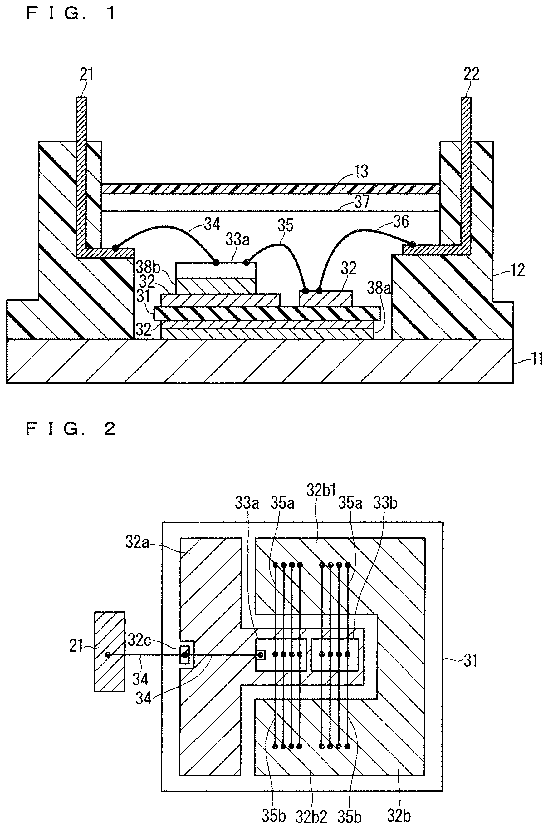
Description will be made below based on the assumption that a semiconductor device according to Embodiment 1 is a semiconductor module. is a cross-sectional view illustrating a schematic configuration of the semiconductor device according to Embodiment 1. illustrates the schematic configuration of the semiconductor device, and thus slightly differs from and subsequent drawings.
The semiconductor device in includes a base plate 11 , a case 12 , a lid 13 , an external control terminal 21 , an external connection terminal 22 , an insulating substrate 31 , a plurality of circuit patterns 32 , a first semiconductor element 33 a , a control wire 34 , an emitter wire 35 , a connection wire 36 , and a sealing member 37 . As with the first semiconductor element 33 a , the semiconductor device includes a second semiconductor element 33 b , although the second semiconductor element 33 b is not illustrated in .
The case 12 is disposed on the base plate 11 made of metal, such as copper, and surrounds a portion of the base plate 11 . The base plate 11 and the case 12 constitute a container body containing the first semiconductor element 33 a and the like in an internal space. The lid 13 blocks an opening of the case 12 to seal the internal space of the container body.
The external control terminal 21 and the external connection terminal 22 are each formed of a metal plate, for example. One end of the external control terminal 21 is located external to the case 12 , and is connected to the exterior (e.g., an external terminal) of the semiconductor device. The other end of the external control terminal 21 is located internal to the case 12 , that is, in the internal space of the container body, and is connected to a component internal to the semiconductor device. Similarly, one end of the external connection terminal 22 is located external to the case 12 , and the other end of the external connection terminal 22 is located internal to the case 12 .
The circuit patterns 32 made of metal are arranged on an upper surface and a lower surface of the insulating substrate 31 . A plurality of circuit patterns 32 spaced apart from one another are arranged on the upper surface of the insulating substrate 31 . The insulating substrate 31 is connected to the portion of the base plate 11 surrounded by the case 12 through a circuit pattern 32 on the lower surface of the insulating substrate 31 and solder 38 a.
The first semiconductor element 33 a is connected to the insulating substrate 31 through the circuit patterns 32 on the upper surface and solder 38 b . The first semiconductor element 33 a is a semiconductor switching element, such as an insulated gate bipolar transistor (IGBT) and a metal oxide semiconductor field effect transistor (MOSFET).
The control wire 34 connects a portion of the external control terminal 21 located in the internal space and a control electrode (e.g., gate electrode) disposed on the first semiconductor element 33 a . The emitter wire 35 connects a controlled electrode (e.g., an emitter electrode) disposed on the first semiconductor element 33 a and a circuit pattern 32 . The connection wire 36 connects the circuit pattern 32 to which the emitter wire 35 is connected and a portion of the external connection terminal 22 located in the internal space.
The sealing member 37 is a gel, for example, and seals the insulating substrate 31 , the plurality of circuit patterns 32 , the first semiconductor element 33 a , the control wire 34 , the emitter wire 35 , the connection wire 36 , and the like.
is a plan view illustrating a configuration of the semiconductor device according to Embodiment 1, and is a side view illustrating a configuration of the semiconductor device according to Embodiment 1. A portion of the configuration in is illustrated in each of .
The circuit patterns 32 on the upper surface of the insulating substrate 31 in include a collector pattern 32 a , an emitter pattern 32 b , and a control pattern 32 c in . For example, wet etching allowing for formation of a pattern having a width of approximately 1 mm is used to form the circuit patterns 32 including the collector pattern 32 a , the emitter pattern 32 b , and the control pattern 32 c.
The collector pattern 32 a is a circuit pattern 32 connected to the first semiconductor element 33 a through the solder 38 b . As with the first semiconductor element 33 a , the second semiconductor element 33 b connected to the collector pattern 32 a through the solder 38 b is illustrated in . The second semiconductor element 33 b is a diode, such as a PN junction diode (PND) and a Schottky barrier diode (SBD).
The emitter pattern 32 b is a conductive member including a first opposing portion 32 b 1 and a second opposing portion 32 b 2 . The first opposing portion 32 b 1 and the second opposing portion 32 b 2 are located opposite each other with respect to the first semiconductor element 33 a in plan view. The second opposing portion 32 b 2 is located directly opposite the first opposing portion 32 b 1 with respect to the first semiconductor element 33 a in the example of , but the location is not limited to this location as will be described below. The first opposing portion 32 b 1 and the second opposing portion 32 b 2 are electrically connected to each other, and have the same potential.
The control pattern 32 c is connected only to the control wire 34 between the external control terminal 21 and the first semiconductor element 33 a.
The emitter wire 35 in includes a first emitter wire 35 a as a first wire and a second emitter wire 35 b as a second wire in .
The first emitter wire 35 a is connected to the controlled electrode on the first semiconductor element 33 a and the first opposing portion 32 b 1 . The second emitter wire 35 b is connected to the controlled electrode on the first semiconductor element 33 a and the second opposing portion 32 b 2 .
As illustrated in , the second emitter wire 35 b is located opposite the first emitter wire 35 a with respect to a connection point where the first emitter wire 35 a and the first semiconductor element 33 a are connected to each other in plan view. In Embodiment 1, a direction of extension of the first emitter wire 35 a and a direction of extension of the second emitter wire 35 b form a straight angle (an angle of 180°) in plan view. As will be described in Embodiment 7, however, the direction of extension of the first emitter wire 35 a and the direction of extension of the second emitter wire 35 b may form an obtuse angle (an angle more than 90° and less than 180°) in plan view.
The first emitter wire 35 a and the second emitter wire 35 b are a single stitch-bonded wire in the example of , but the first emitter wire 35 a and the second emitter wire 35 b are not limited to the single stitch-bonded wire, and may be separated from each other.
As with the first semiconductor element 33 a , the second semiconductor element 33 b is connected to the first opposing portion 32 b 1 with the first emitter wire 35 a , and is connected to the second opposing portion 32 b 2 with the second emitter wire 35 b.
is a circuit diagram corresponding to the configuration of . The diode as the second semiconductor element 33 b is connected in parallel with the semiconductor switching element as the first semiconductor element 33 a , and functions as a freewheeling diode.
Collector wiring 41 in corresponds to the collector pattern 32 a in . Emitter wiring 42 in corresponds to the emitter pattern 32 b , the first emitter wire 35 a , and the second emitter wire 35 b in . Control wiring 43 in corresponds to the control pattern 32 c and the control wire 34 in .
Summary of Embodiment 1
According to the semiconductor device according to Embodiment 1 as described above, the second emitter wire 35 b is located opposite the first emitter wire 35 a with respect to the connection point where the first emitter wire 35 a and the first semiconductor element 33 a are connected to each other in plan view. According to such a configuration, a wire can be bonded to the emitter pattern 32 b , the first semiconductor element 33 a , and the emitter pattern 32 b , which are arranged substantially in a straight line, in the stated order. The wire can thus be bonded even when a sufficient number of wires cannot be bonded to the first semiconductor element 33 a in a normal case. The number of wires and heat generation of a wire can be maintained without increasing the size of the semiconductor device, so that reliability of wiring can be improved.
In Embodiment 1, the emitter pattern 32 b is disposed on the insulating substrate 31 to which the first semiconductor element 33 a is connected. This can reduce a space for insulation between the first semiconductor element 33 a and the emitter pattern 32 b in plan view, so that the semiconductor device can be miniaturized. Furthermore, the layout of the emitter pattern 32 b can easily be changed, so that versatility in the manufacture of the semiconductor device can be increased.
The semiconductor device according to Embodiment 1 includes the control pattern 32 c , but may not include the control pattern 32 c . A degree of freedom of a design layout, however, can be increased by including the control pattern 32 c , so that further miniaturization of the semiconductor device can be expected. The semiconductor device according to Embodiment 1 includes the second semiconductor element 33 b , but may not include the second semiconductor element 33 b.
Embodiment 2
is a plan view illustrating a configuration of a semiconductor device according to Embodiment 2, and corresponds to .
As illustrated in , the semiconductor device according to Embodiment 2 includes a plurality of first semiconductor elements 33 a and a plurality of second semiconductor elements 33 b , but does not include the control pattern 32 c.
Each of the plurality of first semiconductor elements 33 a is connected to the emitter pattern 32 b with the first emitter wire 35 a and the second emitter wire 35 b as with the first semiconductor element 33 a in Embodiment 1. The plurality of first semiconductor elements 33 a are thereby connected in parallel with one another with a plurality of first emitter wires 35 a , a plurality of second emitter wires 35 b , and the emitter pattern 32 b , and thus can be driven in parallel with one another. Similarly, the plurality of second semiconductor elements 33 b are connected in parallel with one another with a plurality of first emitter wires 35 a , a plurality of second emitter wires 35 b , and the emitter pattern 32 b.
According to the semiconductor device according to Embodiment 2 as described above, the plurality of first semiconductor elements 33 a can be driven in parallel with one another, so that an increase in capacity of the semiconductor device can be expected.
Embodiment 3
are plan views each illustrating a configuration of a semiconductor device according to Embodiment 3, and correspond to .
The configuration in Embodiment 3 is similar to the configuration in Embodiment 2 in to which the control pattern 32 c has been added. The plurality of first semiconductor elements 33 a may be provided with respective control patterns 32 c as illustrated in , or the plurality of first semiconductor elements 33 a may share a single control pattern 32 c as illustrated in . According to such a configuration, the degree of freedom of the design layout can be increased more than that of the configuration in Embodiment 2, so that miniaturization of the semiconductor device can be expected.
When the control pattern 32 c is disposed at an end of another circuit pattern 32 , such as the collector pattern 32 a , as in Embodiment 3, the likelihood of the control wire 34 being electrically connected to the other circuit pattern 32 can be reduced.
Embodiment 4
is a plan view illustrating a configuration of a semiconductor device according to Embodiment 4, and corresponds to . is a side view illustrating a configuration of the semiconductor device according to Embodiment 4, and corresponds to .
As illustrated in , the control wire 34 between control electrodes of the plurality of first semiconductor elements 33 a is stitch-bonded to the control electrodes in Embodiment 4. Thus, in Embodiment 4, the plurality of first semiconductor elements 33 a are not provided with respective control wires 34 , but provided with a single control wire 34 . The control wire 34 is only required to be stitch-bonded to one or more control electrodes. According to the semiconductor device according to Embodiment 4 as described above, wiring with the control wire 34 is easy.
As illustrated in , the control wire 34 passes above between an end of the first emitter wire 35 a remote from the second emitter wire 35 b and an end of the second emitter wire 35 b remote from the first emitter wire 35 a in Embodiment 4. According to such a configuration, wiring with the control wire 34 is easy. When the first emitter wire 35 a and the second emitter wire 35 b are separated from each other in contrast to the example of , the control wire 34 may pass above a portion between the first emitter wire 35 a and the second emitter wire 35 b.
Embodiment 5
is a plan view illustrating a configuration of a semiconductor device according to Embodiment 5, and corresponds to .
As illustrated in , the second semiconductor element 33 b is connected to the first emitter wire 35 a between the first semiconductor element 33 a and the first opposing portion 32 b 1 or to the second emitter wire 35 b between the first semiconductor element 33 a and the second opposing portion 32 b 2 in Embodiment 5.
According to the semiconductor device according to Embodiment 5 as described above, the first semiconductor element 33 a and the second semiconductor element 33 b share the first emitter wire 35 a or the second emitter wire 35 b . The number of wires of the semiconductor device as a whole can thereby be reduced, so that miniaturization or an increase in capacity of the semiconductor device can be expected.
Embodiment 6
is a plan view illustrating a configuration of a semiconductor device according to Embodiment 6, and corresponds to . is a side view illustrating a configuration of the semiconductor device according to Embodiment 6, and corresponds to .
The conductive member according to each of Embodiments 1 to 5 is the emitter pattern 32 b including the first opposing portion 32 b 1 and the second opposing portion 32 b 2 . In contrast, the conductive member according to Embodiment 6 includes an emitter pattern 32 b not including the first opposing portion 32 b 1 and the second opposing portion 32 b 2 , a first copper block 32 b 3 , and a second copper block 32 b 4 as illustrated in .
As illustrated in , the first copper block 32 b 3 and the second copper block 32 b 4 respectively correspond to the first opposing portion 32 b 1 and the second opposing portion 32 b 2 , and are arranged on the emitter pattern 32 b through solder 38 c . When the first copper block 32 b 3 and the second copper block 32 b 4 cannot be supported only by the solder 38 c , an insulating member 39 may be disposed between the collector pattern 32 a and each of the first copper block 32 b 3 and the second copper block 32 b 4 as illustrated in . As illustrated in , a plurality of first copper blocks 32 b 3 and a plurality of second copper blocks 32 b 4 may be arranged.
According to the semiconductor device according to Embodiment 6 as described above, the emitter pattern 32 b not including the first opposing portion 32 b 1 and the second opposing portion 32 b 2 can be used. This can reduce a space for insulation between the first semiconductor element 33 a and each of the first opposing portion 32 b 1 and the second opposing portion 32 b 2 in plan view, so that the semiconductor device can be miniaturized.
Embodiment 7
is a plan view illustrating a configuration of a semiconductor device according to Embodiment 7, and corresponds to .
In each of Embodiments 1 and 6, the second opposing portion 32 b 2 is located directly opposite the first opposing portion 32 b 1 with respect to the first semiconductor element 33 a in plan view. The direction of extension of the first emitter wire 35 a and the direction of extension of the second emitter wire 35 b form the straight angle in plan view.
In contrast, as illustrated in , the second opposing portion 32 b 2 is offset from the location directly opposite the first opposing portion 32 b 1 with respect to the first semiconductor element 33 a in Embodiment 7. The direction of extension of the first emitter wire 35 a and the direction of extension of the second emitter wire 35 b form an obtuse angle, and an angle θ between them is more than 90° and less than 180°.
According to the semiconductor device according to Embodiment 7 as described above, the degree of freedom of the design layout can be increased without impairing reliability of wiring, so that miniaturization or an increase in capacity of the semiconductor device can be expected.
Embodiment 8
In Embodiment 8, at least one of the first semiconductor element 33 a and the second semiconductor element 33 b includes a wide bandgap semiconductor. The wide bandgap semiconductor includes silicon carbide (SiC), gallium nitride (GaN), and diamond, for example. According to Embodiment 8 as described above, miniaturization and parallelization of the semiconductor device can be expected.
Embodiments and modifications can freely be combined with each other, and can be modified or omitted as appropriate.
While the invention has been shown and described in detail, the foregoing description is in all aspects illustrative and not restrictive. It is therefore understood that numerous modifications and variations can be devised without departing from the scope of the invention.
Figures (10)
Citations
This patent cites (8)
- US20150214126
- US20200119179
- USH07-058272
- USH08-078619
- US2009-206140
- US2015-076511
- US2017-107937
- US2018-186302