Pixel Drive Circuit, Driving Method, and Display Panel
Abstract
Disclosed are a pixel drive circuit, a driving method, and a display panel. The pixel drive circuit includes a light-emitting element, a power supply line, and a pulse amplitude modulation unit and a pulse width modulation unit connected between a high-potential power supply of the power supply line and an anode of the light emitting element. The pulse amplitude modulation unit provides driving currents with different amplitudes to the light emitting element. The pulse width modulation unit includes a second drive transistor, a first transistor and a second transistor, and a pulse width modulation circuit. The pulse width modulation circuit generates a corresponding drive signal to control the first transistor or the second transistor to be turned on based on the first data voltages during a luminescence phase, and controls the second drive transistor to be turned on to control the duration of the driving currents of the light-emitting element.
Claims (19)
1. A pixel drive circuit, comprising: a power supply line, comprising a high-potential power supply and a low-potential power supply; a light-emitting element; connected between the high-potential power supply and the low-potential power supply; a pulse amplitude modulation unit, comprising: a first drive transistor connected to an anode of the light-emitting element and the high-potential power supply, and a pulse amplitude modulation circuit connected to a control end of the first drive transistor; wherein the first drive transistor is configured to provide driving currents with different amplitudes to the light-emitting element according to a voltage applied at the control end by the pulse amplitude modulation circuit; and a pulse width modulation unit, comprising: a second drive transistor, connected to the anode of the light-emitting element and the pulse amplitude modulation unit; a first transistor and a second transistor, connected to a control end of the second drive transistor; a pulse width modulation circuit, connected to a control end of the first transistor and a control end of the second transistor; wherein a first end of the first transistor is connected to the high-potential power supply, a second end of the first transistor is connected to a first end of the second transistor, and the control end of the first transistor is connected to the pulse width modulation circuit; a second end of the second transistor is connected to the low-potential power supply, and the control end of the second transistor is connected to the pulse width modulation circuit; a third transistor; wherein a first end of the third transistor is connected to a first data line to receive first data voltages of different voltage levels output from the first data line, and a second end of the third transistor is connected to a first node; a fourth transistor; wherein a first end of the fourth transistor is connected to a second data line to receive a second data voltage output from the second data line, a second end of the fourth transistor is connected to a control end of the third transistor, and a control end of the fourth transistor is connected to a first scan control line; and a first capacitor; wherein a first pole plate of the first capacitor is connected to the low-potential power supply, and a second pole plate of the first capacitor is connected to the control end of the third transistor; wherein the second drive transistor is of a same type as the first transistor, one of the first transistor and the second transistor being a P-type transistor, and the other of the first transistor and the second transistor being an N-type transistor; the pulse width modulation circuit is configured to output the first data voltages of different voltage levels with the first data line during a luminescence phase, for generating corresponding drive signals to control the first transistor or second transistor to be turned on, and controlling the second drive transistor to be turned on to control a duration of the driving currents of the light-emitting element.
9. A driving method of a pixel drive circuit; wherein the pixel drive circuit comprises: a power supply line, comprising a high-potential power supply and a low-potential power supply; a light-emitting element; connected between the high-potential power supply and the low-potential power supply; a pulse amplitude modulation unit, comprising: a first drive transistor connected to an anode of the light-emitting element and the high-potential power supply, and a pulse amplitude modulation circuit connected to a control end of the first drive transistor; and a pulse width modulation unit, comprising: a second drive transistor, connected to the anode of the light-emitting element and the pulse amplitude modulation unit; a first transistor and a second transistor, connected to a control end of the second drive transistor; a pulse width modulation circuit, connected to a control end of the first transistor and a control end of the second transistor; wherein a first end of the first transistor is connected to the high-potential power supply, a second end of the first transistor is connected to a first end of the second transistor, and the control end of the first transistor is connected to the pulse width modulation circuit; a second end of the second transistor is connected to the low-potential power supply, and the control end of the second transistor is connected to the pulse width modulation circuit; a third transistor; wherein a first end of the third transistor is connected to a first data line to receive first data voltages of different voltage levels output from the first data line, and a second end of the third transistor is connected to a first node; a fourth transistor; wherein a first end of the fourth transistor is connected to a second data line to receive a second data voltage output from the second data line, a second end of the fourth transistor is connected to a control end of the third transistor, and a control end of the fourth transistor is connected to a first scan control line; and a first capacitor; wherein a first pole plate of the first capacitor is connected to the low-potential power supply, and a second pole plate of the first capacitor is connected to the control end of the third transistor; wherein the second drive transistor is of a same type as the first transistor, one of the first transistor and the second transistor being a P-type transistor, and the other of the first transistor and the second transistor being an N-type transistor; wherein the method comprises: during a reset phase, providing, by the first drive transistor, driving currents with different amplitudes to the light-emitting element according to a voltage applied at the control end by the pulse amplitude modulation circuit; and during a luminescence phase, outputting, by the pulse width modulation circuit, the first data voltages of different voltage levels with the first data line, for generating corresponding drive signals to control the first transistor or second transistor to be turned on and controlling the second drive transistor to be turned on to control a duration of the driving currents of the light-emitting element.
12. A display panel, comprising a plurality of pixel cells arranged in an array; wherein each pixel cell is arranged with a pixel drive circuit comprising: a power supply line, comprising a high-potential power supply and a low-potential power supply; a light-emitting element; connected between the high-potential power supply and the low-potential power supply; a pulse amplitude modulation unit, comprising: a first drive transistor connected to an anode of the light-emitting element and the high-potential power supply, and a pulse amplitude modulation circuit connected to a control end of the first drive transistor; wherein the first drive transistor is configured to provide driving currents with different amplitudes to the light-emitting element according to a voltage applied at the control end by the pulse amplitude modulation circuit; and a pulse width modulation unit, comprising: a second drive transistor, connected to the anode of the light-emitting element and the pulse amplitude modulation unit; a first transistor and a second transistor, connected to a control end of the second drive transistor; a pulse width modulation circuit, connected to a control end of the first transistor and a control end of the second transistor; wherein a first end of the first transistor is connected to the high-potential power supply, a second end of the first transistor is connected to a first end of the second transistor, and the control end of the first transistor is connected to the pulse width modulation circuit; a second end of the second transistor is connected to the low-potential power supply, and the control end of the second transistor is connected to the pulse width modulation circuit; a third transistor; wherein a first end of the third transistor is connected to a first data line to receive first data voltages of different voltage levels output from the first data line, and a second end of the third transistor is connected to a first node; a fourth transistor; wherein a first end of the fourth transistor is connected to a second data line to receive a second data voltage output from the second data line, a second end of the fourth transistor is connected to a control end of the third transistor, and a control end of the fourth transistor is connected to a first scan control line; and a first capacitor; wherein a first pole plate of the first capacitor is connected to the low-potential power supply, and a second pole plate of the first capacitor is connected to the control end of the third transistor; wherein the second drive transistor is of a same type as the first transistor, one of the first transistor and the second transistor being a P-type transistor, and the other of the first transistor and the second transistor being an N-type transistor; the pulse width modulation circuit is configured to output the first data voltages of different voltage levels with the first data line during a luminescence phase, for generating corresponding drive signals to control the first transistor or second transistor to be turned on, and controlling the second drive transistor to be turned on to control a duration of the driving currents of the light-emitting element.
Show 16 dependent claims
2. The pixel drive circuit according to claim 1 , wherein the pulse width modulation unit further comprises a reset transistor; a first end of the reset transistor is connected to the first node, a second end of the reset transistor is connected to the low-potential power supply, and a control end of the reset transistor is connected to a reset control line; wherein the first node is a point where the pulse width modulation circuit is connected to the control end of the first transistor and the control end of the second transistor.
3. The pixel drive circuit according to claim 1 , wherein the third transistor is a P-type transistor; for one of the first data voltages of different voltage levels, in response to a voltage sum of the first data voltage of a voltage level output and a threshold voltage of third transistor being less than the second data voltage, the third transistor is turned off; in response to the voltage sum of the first data voltage of the voltage level and the threshold voltage of the third transistor being greater than the second data voltage, the third transistor is turned on; wherein a turned-on time of the second drive transistor is associated with a magnitude of the second data voltage and a magnitude of the first data voltages of different levels.
4. The pixel drive circuit according to claim 1 , wherein the pulse width modulation circuit further comprises a second capacitor; a first pole plate of the second capacitor is connected to the high-potential power supply, and a second pole plate of the second capacitor is connected to the first node.
5. The pixel drive circuit according to claim 1 , wherein the pulse amplitude modulation circuit comprises a fifth transistor and a third capacitor; a first end of the fifth transistor is connected to a third data line, a second end of the fifth transistor is connected to the control end of the first drive transistor, and a control end of the fifth transistor is connected to a second scan control line; a first pole plate of the third capacitor is connected to the high-potential power supply, and a second pole plate of the third capacitor is connected to the control end of the first drive transistor.
6. The pixel drive circuit according to claim 1 , wherein the pulse amplitude modulation circuit comprises a fifth transistor; a first end of the fifth transistor is connected to a third data line, a second end of the fifth transistor is connected to the control end of the first drive transistor, and a control end of the fifth transistor is connected to a second scan control line; wherein the first data line, the second data line, and the third data line are multiplexed.
7. The pixel drive circuit according to claim 1 , wherein the different voltage levels of the first data voltages are stepped up or stepped down.
8. The pixel drive circuit according to claim 1 , wherein the duration of the different voltage levels of the first data voltages is the same.
10. The driving method according to claim 9 , wherein a turned-on time of the second drive transistor is associated with a magnitude of the second data voltage and a magnitude of the first data voltages of different levels.
11. The driving method according to claim 10 , wherein the third transistor is a P-type transistor; for one of the first data voltages of different voltage levels, in response to a voltage sum of the first data voltage of a voltage level output and a threshold voltage of third transistor being less than the second data voltage, the third transistor is turned off; in response to the voltage sum of the first data voltage of the voltage level and the threshold voltage of the third transistor being greater than the second data voltage, the third transistor is turned on.
13. The display panel according to claim 12 , wherein the pulse width modulation unit further comprises a reset transistor; a first end of the reset transistor is connected to the first node, a second end of the reset transistor is connected to the low-potential power supply, and a control end of the reset transistor is connected to a reset control line; wherein the first node is a point where the pulse width modulation circuit is connected to the control end of the first transistor and the control end of the second transistor.
14. The display panel according to claim 12 , wherein the third transistor is a P-type transistor; for one of the first data voltages of different voltage levels, in response to a voltage sum of the first data voltage of a voltage level output and a threshold voltage of third transistor being less than the second data voltage, the third transistor is turned off; in response to the voltage sum of the first data voltage of the voltage level and the threshold voltage of the third transistor being greater than the second data voltage, the third transistor is turned on; wherein a turned-on time of the second drive transistor is associated with a magnitude of the second data voltage and a magnitude of the first data voltages of different levels.
15. The display panel according to claim 12 , wherein the pulse width modulation circuit further comprises a second capacitor; a first pole plate of the second capacitor is connected to the high-potential power supply, and a second pole plate of the second capacitor is connected to the first node.
16. The display panel according to claim 12 , wherein the pulse amplitude modulation circuit comprises a fifth transistor and a third capacitor; a first end of the fifth transistor is connected to a third data line, a second end of the fifth transistor is connected to the control end of the first drive transistor, and a control end of the fifth transistor is connected to a second scan control line; a first pole plate of the third capacitor is connected to the high-potential power supply, and a second pole plate of the third capacitor is connected to the control end of the first drive transistor.
17. The display panel according to claim 12 , wherein the pulse amplitude modulation circuit comprises a fifth transistor; a first end of the fifth transistor is connected to a third data line, a second end of the fifth transistor is connected to the control end of the first drive transistor, and a control end of the fifth transistor is connected to a second scan control line; wherein the first data line, the second data line, and the third data line are multiplexed.
18. The display panel according to claim 12 , wherein the different voltage levels of the first data voltages are stepped up or stepped down.
19. The display panel according to claim 12 , wherein the duration of the different voltage levels of the first data voltages is the same.
Full Description
Show full text →
CROSS REFERENCE
The present application claims priority of China Patent Application No. 202211633060.8 filed on Dec. 19, 2022, the entire contents of which are hereby incorporated by reference.
TECHNICAL FIELD
The present disclosure relates to the field of display panels, and in particular to a pixel drive circuit, a driving method, and a display panel.
BACKGROUND
Currently, inorganic micro light emitting diode (Micro LED) displays are one of the hot spots in display research.
Compared with OLED displays, Micro LEDs have the advantages of high reliability, low power consumption, high brightness, and fast response time, etc. Among them, the drive circuit for controlling the LED light emission is the core technology of Micro LED display and has important research significance.
However, since the luminous efficiency of LEDs varies greatly under different driving currents, in order to reduce the power consumption of Micro LED displays, it is necessary to maintain the LEDs working at relatively high currents for keeping the LEDs always in a high-efficiency operating range, thereby achieving gray-scale cutting.
SUMMARY OF THE DISCLOSURE
The main technical problem solved by the present disclosure is to provide a pixel drive circuit and its driving method, and a display panel to realize the light-emitting element to maintain in a high-efficiency working range, thereby achieving gray-scale cutting.
To solve the above technical problem, the present disclosure provides a pixel drive circuit, including: a power supply line, comprising a high-potential power supply and a low-potential power supply; a light-emitting element; connected between the high-potential power supply and the low-potential power supply; a pulse amplitude modulation unit, comprising: a first drive transistor connected to an anode of the light-emitting element and the high-potential power supply, and a pulse amplitude modulation circuit connected to a control end of the first drive transistor; wherein the first drive transistor is configured to provide driving currents with different amplitudes to the light-emitting element according to a voltage applied at the control end by the pulse amplitude modulation circuit; and a pulse width modulation unit, comprising: a second drive transistor, connected to the anode of the light-emitting element and the pulse amplitude modulation unit; a first transistor and a second transistor, connected to a control end of the second drive transistor; a pulse width modulation circuit, connected to a control end of the first transistor and a control end of the second transistor; wherein a first end of the first transistor is connected to the high-potential power supply, a second end of the first transistor is connected to a first end of the second transistor, and the control end of the first transistor is connected to the pulse width modulation circuit; a second end of the second transistor is connected to the low-potential power supply, and the control end of the second transistor is connected to the pulse width modulation circuit; a third transistor; wherein a first end of the third transistor is connected to a first data line to receive first data voltages of different voltage levels output from the first data line, and a second end of the third transistor is connected to a first node; a fourth transistor; wherein a first end of the fourth transistor is connected to a second data line to receive a second data voltage output from the second data line, a second end of the fourth transistor is connected to a control end of the third transistor, and a control end of the fourth transistor is connected to a first scan control line; and a first capacitor; wherein a first pole plate of the first capacitor is connected to the low-potential power supply, and a second pole plate of the first capacitor is connected to the control end of the third transistor; wherein the second drive transistor is of a same type as the first transistor, one of the first transistor and the second transistor being a P-type transistor, and the other of the first transistor and the second transistor being an N-type transistor; the pulse width modulation circuit is configured to output the first data voltages of different voltage levels with the first data line during a luminescence phase, for generating corresponding drive signals to control the first transistor or second transistor to be turned on, and controlling the second drive transistor to be turned on to control a duration of the driving currents of the light-emitting element.
In some embodiments, the pulse width modulation unit further comprises a reset transistor; a first end of the reset transistor is connected to the first node, a second end of the reset transistor is connected to the low-potential power supply, and a control end of the reset transistor is connected to a reset control line; wherein the first node is a point where the pulse width modulation circuit is connected to the control end of the first transistor and the control end of the second transistor.
In some embodiments, the third transistor is a P-type transistor; for one of the first data voltages of different voltage levels, in response to a voltage sum of the first data voltage of a voltage level output and a threshold voltage of third transistor being less than the second data voltage, the third transistor is turned off; in response to the voltage sum of the first data voltage of the voltage level and the threshold voltage of the third transistor being greater than the second data voltage, the third transistor is turned on; wherein a turned-on time of the second drive transistor is associated with a magnitude of the second data voltage and a magnitude of the first data voltages of different levels.
In some embodiments, the pulse width modulation circuit further comprises a second capacitor; a first pole plate of the second capacitor is connected to the high-potential power supply, and a second pole plate of the second capacitor is connected to the first node.
In some embodiments, the pulse amplitude modulation circuit comprises a fifth transistor and a third capacitor; a first end of the fifth transistor is connected to a third data line, a second end of the fifth transistor is connected to the control end of the first drive transistor, and a control end of the fifth transistor is connected to a second scan control line; a first pole plate of the third capacitor is connected to the high-potential power supply, and a second pole plate of the third capacitor is connected to the control end of the first drive transistor.
In some embodiments, the pulse amplitude modulation circuit comprises a fifth transistor; a first end of the fifth transistor is connected to a third data line, a second end of the fifth transistor is connected to the control end of the first drive transistor, and a control end of the fifth transistor is connected to a second scan control line; wherein the first data line, the second data line, and the third data line are multiplexed.
To solve the above technical problem, the present disclosure further provides a driving method of a pixel drive circuit, applied to the pixel drive circuit in any of the above embodiment and including: during a reset phase, outputting, by a reset control line of an Nth row, a reset signal to control a reset transistor to be turned on, and outputting, by a low-potential power supply, a low-potential voltage to a control end of a first transistor through the reset transistor, for causing the first transistor to be turned on; during a data writing phase, outputting, by a first scan control line of an Nth row, a first scan signal to control a fourth transistor to be turned on, and outputting, by a second data line, a second data voltage to a control end of a third transistor through the fourth transistor; outputting, by a second scan control line of an Nth row, a second scan signal to control a fifth transistor to be turned on, and outputting, by a third data line, a third data voltage to a control end of a first drive transistor through the fifth transistor; and during a luminescence phase, outputting, by a first data line, first data voltages of different voltage levels to the control end of the first transistor and a control end of a second transistor, selectively, through the third transistor, for controlling the first transistor or the second transistor to be turned on, and further controlling the second drive transistor to be turned on to control a duration of a driving current of a light-emitting element.
In some embodiments, a turned-on time of the second drive transistor is associated with a magnitude of the second data voltage and a magnitude of the first data voltages of different levels.
To solve the above technical problem, the present disclosure further provides a display panel, including a plurality of pixel cells arranged in an array; wherein each pixel cell is arranged with the pixel drive circuit in any of the above embodiments.
The beneficial effect of the present disclosure is that, in contrast to the related art, the driving currents of the light-emitting element are modulated by controlling the voltage at the control end of the first drive transistor of the pulse amplitude modulation unit. The pulse width modulation unit includes a second drive transistor connected in series to the anode of the light-emitting element and the pulse amplitude modulation unit; a first transistor and a second transistor connected to the control end of the second drive transistor; and a pulse width modulation circuit, connected to the control end of the first transistor and the control end of the second transistor; wherein a first end of the first transistor is connected to the high-potential power supply, a second end of the first transistor is connected to a first end of the second transistor, and the control end of the first transistor is connected to the pulse width modulation circuit; a second end of the second transistor is connected to the low-potential power supply, and the control end of the second transistor is connected to the pulse width modulation circuit; the second drive transistor is of a same type as the first transistor, one of the first transistor and the second transistor being a P-type transistor, and the other of the first transistor and the second transistor being an N-type transistor; the pulse width modulation circuit is connected to a first data line to output the first data voltages of different voltage levels with the first data line during a luminescence phase, for generating corresponding drive signals to control the first transistor or second transistor to be turned on, and controlling the second drive transistor to be turned on to control a duration of the driving currents of the light-emitting element. In this way, the light-emitting element may maintain in a high-efficiency working range, thereby achieving gray-scale cutting.
BRIEF DESCRIPTION OF THE DRAWINGS
In order to more clearly illustrate the technical solutions in the embodiments of the present disclosure, the following will briefly describe the accompanying drawings required in the description of the embodiments, it is obvious that the following description of the accompanying drawings are only some of the embodiments of the present disclosure. For those skilled in the art, other accompanying drawings may be obtained from these drawings without creative labor.
is a structural block view of a pixel drive circuit according to an embodiment of the present disclosure.
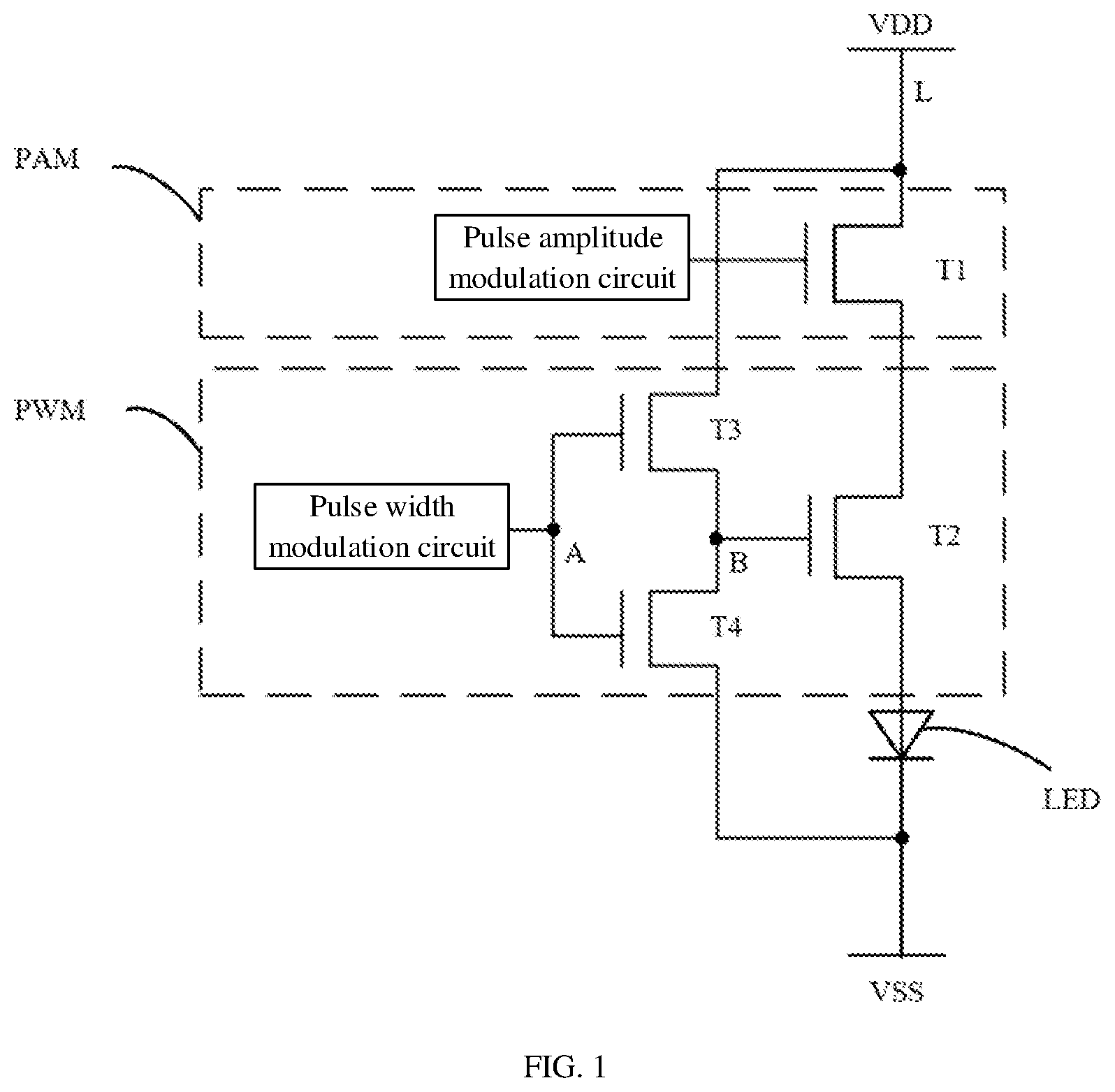
is a structural schematic view of a pixel drive circuit according to a first embodiment of the present disclosure.
is a timing diagram of drive signals of a pixel drive circuit according to an embodiment of the present disclosure.
is a correspondence schematic view between a first data voltage, a third data voltage, and a gray scale according to an embodiment of the present disclosure.
is a correspondence schematic view between a first data voltage, a third data voltage, and a gray scale according to another embodiment of the present disclosure.
is a structural schematic view of a pixel drive circuit according to a second embodiment of the present disclosure.
is a flowchart of a driving method of a pixel drive circuit according to an embodiment of the present disclosure.
is an equivalent circuit diagram of a driving method of a pixel drive circuit during a reset phase according to an embodiment of the present disclosure.
is an equivalent circuit diagram of a driving method of a pixel drive circuit during a data writing phase according to an embodiment of the present disclosure.
is an equivalent circuit diagram of a driving method of a pixel drive circuit in a first stage during a luminescence phase according to an embodiment of the present disclosure.
is an equivalent circuit diagram of a driving method of a pixel drive circuit in a second stage during a luminescence phase according to an embodiment of the present disclosure.
is a structural schematic view of a display panel according to an embodiment of the present disclosure.
NUMERAL REFERENCE
•
• LED, light-emitting element; • L, power supply line; VDD, high-potential power supply line; VSS, low-potential power supply line; • PAM, pulse amplitude modulation unit; T 8 , fifth transistor; C 1 , third capacitor; • PWM, pulse width modulation unit; T 1 , first drive transistor; T 2 , second drive transistor; T 3 , first transistor; T 4 , second transistor; T 5 , reset transistor; T 6 , third transistor; T 7 , fourth transistor; C 1 , first capacitor; C 2 , second capacitor; • L_Reset, reset control line; Reset, reset signal; L 1 , first data line; Vdata_ 1 , first data voltage; L 2 , second data line; Vdata_ 2 , second data voltage; L 3 , third data line; Vdata_ 3 , third data voltage; L_Scan 1 , first scan control line; PWM_Scan, first scan signal; L_Scan 2 , second scan control line; PAM_Scan, second scan signal; Vth, threshold voltage; A, first node; B, second node; C, third node; 110 , pixel unit.
DETAILED DESCRIPTION
The following will be a clear and complete description of the technical solutions in the embodiments of the present disclosure, in conjunction with the accompanying drawings in the embodiments of the present disclosure. Obviously, the described embodiments are only a part of the embodiments of the present disclosure, and not all of them. Based on the embodiments in the present disclosure, all other embodiments obtained by those skilled in the art without making creative labor fall within the scope of the present disclosure.
The terms used in the embodiments of the present disclosure are intended solely for the purpose of describing particular embodiments and are not intended to limit the present disclosure. The singular forms of “one”, “said”, and “the” as used in the embodiments of the present disclosure and the appended claims are also intended to include plural forms, unless clearly indicated above. Unless other meanings are clearly indicated above, “a plurality” generally includes at least two, but does not exclude the inclusion of at least one.
It should be understood that the term “and/or” as used herein is simply a description of the association of related objects, indicating that three relationships can exist, e.g., A and/or B, which can mean: A alone, both A and B, and B alone. In addition, the character “/” in this document generally indicates that the associated objects before and after are in an “or” relationship. The terms “first”, “second”, etc. in the specification, claims, and the above-mentioned drawings of the present disclosure are used to distinguish similar objects, and need not be used to describe a specific order or sequence.
It is to be understood that the term “including”, “comprising”, or any other variation thereof, as used herein, is intended to cover non-exclusive inclusion such that a process, method, article, or apparatus including a series of elements includes not only those elements, but may further include other elements not expressly listed, and may further include elements that are inherent to such process, method, article, or apparatus. Without further limitation, the elements defined by the statement “including . . . ” do not preclude the existence of additional identical elements in the process, method, article, or apparatus that include said elements.
It should be noted that when there are directional indications (such as up, down, left, right, forward, backward . . . ) in the present disclosure, the directional indications are intended only to explain the relative positions, movements, etc. of components in a particular posture (as shown in the accompanying drawings), and if that particular posture is changed, the directional indications are also changed accordingly.
References herein to “embodiments” mean that particular features, structures, or characteristics described in connection with the embodiments may be included in at least one embodiment of the present disclosure. The presence of the phrase at each location in the specification does not necessarily mean the same embodiment, nor is it a separate or alternative embodiment that is mutually exclusive with other embodiments. It is understood, both explicitly and implicitly, by those skilled in the art that the embodiments described herein may be combined with other embodiments.
The present disclosure provides a pixel drive circuit. Referring to , is a structural block view of a pixel drive circuit according to an embodiment of the present disclosure. As illustrated in , the pixel drive circuit includes: a light-emitting element LED, a power supply line L, a pulse amplitude modulation unit PAM, and a pulse width modulation unit PWM.
The light-emitting element LED is a light-emitting diode or an organic light-emitting diode.
The power supply line L includes a high-potential power supply VDD and a low-potential power supply VSS. The high-potential power supply VDD is configured to output a high-potential voltage, and the low-potential power supply VSS is configured to output a low-potential voltage. The light-emitting element LED is connected in series between the high-potential power supply VDD and the low-potential power supply VSS, and the light-emitting element LED is turned on and emits light when there is a voltage difference between two ends of the light-emitting element LED. The low-potential power supply VSS may be grounded, without specific limitation herein.
In the embodiments, the high-potential power supply VDD in the power supply line L is connected in series with the pulse amplitude modulation unit PAM, the pulse width modulation unit PWM, the light-emitting element LED, and the low-potential power supply VSS in sequence. In other words, the current flows from the high-potential power supply VDD through the pulse amplitude modulation unit PAM, the pulse width modulation unit PWM, and the anode of the light-emitting element LED, and then flows from the cathode of the light-emitting element LED to the low-potential power supply VSS.
Of course, in other embodiments, the pulse amplitude modulation unit PAM and pulse width modulation unit PWM order may be switched, without specific limitation herein.
In the embodiments, the pulse amplitude modulation unit PAM includes a first drive transistor T 1 connected to the anode of the light-emitting element LED and the high-potential power supply VDD, and a pulse amplitude modulation circuit connected to a control end of the first drive transistor T 1 . The first drive transistor T 1 provides driving currents with different amplitudes to the light-emitting element LED according to a voltage applied at the control end by the pulse amplitude modulation circuit.
The pulse width modulation unit PWM includes a second drive transistor T 2 connected to the anode of the light-emitting element LED and the pulse amplitude modulation unit PAM, a first transistor T 3 and a second transistor T 4 connected to a control end of the second drive transistor T 2 , and a pulse width modulation circuit connected to a control end of the first transistor T 3 and a control end of the second transistor T 4 .
Specifically, a first end of the first transistor T 3 is connected to the high-potential power supply VDD, a second end of the first transistor T 3 is connected to a first end of the second transistor T 4 , and the control end of the first transistor T 3 is connected to the pulse width modulation circuit; a second end of the second transistor T 4 is connected to the low-potential power supply VSS, and the control end of the second transistor T 4 is connected to the pulse width modulation circuit. A point where the pulse width modulation circuit is connected to the control end of the first transistor T 3 and the control end of the second transistor T 4 is defined as a first node A, and a point where the second end of the first transistor T 3 is connected to the first end of the second transistor T 4 is defined as a second node B.
The second drive transistor T 2 is of the same type as the first transistor T 3 , and one of the first transistor T 3 and the second transistor T 4 is a P-type transistor and the other is an N-type transistor; the pulse width modulation circuit is connected to a first data line L 1 and outputs first data voltages Vdata_ 1 of different voltage levels based on the first data line L 1 during a luminescence phase, thereby generating corresponding drive signals to control the first transistor T 3 or second transistor T 4 to be turned on, and thus controlling the second drive transistor T 2 to be turned on, thereby controlling the duration of the driving current I of the light-emitting element LED, that is, the luminescence time and duration of the light-emitting element LED.
In the embodiments, the first drive transistor T 1 , the second drive transistor T 2 , and the first transistor T 3 are each a P-type transistor, and the second transistor T 4 is an N-type transistor. The source (first end) of the first drive transistor T 1 is connected to the high-potential power supply VDD, the drain (second end) of the first drive transistor T 1 is connected to the source (first end) of the second drive transistor T 2 , and the gate (control end) of the first drive transistor T 1 is connected to the pulse amplitude modulation circuit; the drain (second end) of the second drive transistor T 2 is connected to the anode of the light-emitting element LED, and the gate (control end) of the second drive transistor T 2 is connected to the drain (second end) of the first transistor T 3 and the drain (first end) of the second transistor T 4 ; the source (first end) of the first transistor T 3 is connected to the high-potential power supply VDD, and the gate (control end) of the first transistor T 3 is connected to the pulse width modulation circuit; the source (second end) of the second transistor T 4 is connected to the low-potential power supply VSS, and the gate (control end) of the second transistor T 4 is connected to the pulse width modulation circuit; the cathode of the light-emitting element LED is connected to the low-potential power supply VSS.
In other embodiments, when the first transistor T 3 is an N-type transistor, the second drive transistor T 2 is also an N-type transistor, while the second transistor T 4 is a P-type transistor, and the first drive transistor may be a P-type transistor or an N-type transistor. There is no limitation in this regard, and the specific connection relationship is determined according to the type of each transistor.
The beneficial effect of the present embodiments is that the first transistor T 3 and the second transistor T 4 are arranged to be different types of transistors, such that they can be turned on or off respectively based on different drive signals generated by the pulse width modulation circuit, and then control the second driving transistor T 2 to be turned on when the first transistor T 3 or the second transistor T 4 is turned on. In this way, the pulse width regulation may be realized, such that the light-emitting element LED may maintain in the high-efficiency working range, facilitating the realization of gray-scale cutting.
Combined with , is a structural schematic view of a pixel drive circuit according to a first embodiment of the present disclosure.
In the embodiments, the pulse width modulation unit PWM further includes a reset transistor T 5 , a first end of the reset transistor T 5 is connected to the first node A, a second end of the reset transistor T 5 is connected to the low-potential power supply VSS, and a control end of the reset transistor T 5 is connected to the reset control line L_Reset. The reset control line L_Reset is configured to output a reset signal Reset during a reset phase, for controlling the reset transistor T 5 to be turned on, thereby writing a low-potential voltage to the first node A. By resetting the first node A before each luminescence phase, the control ends of the first transistor T 3 and the second transistor T 4 have the same collimated voltage to facilitate the regulation of the pulse width and avoid the uncontrolled duration of light-emitting element LED at each light emission.
In the embodiments, the reset transistor T 5 is a P-type transistor, the source (second end) of the reset transistor T 5 is connected to the low-potential power supply VSS, the drain (first end) of the reset transistor T 5 is connected to the first node A, and the gate (control end) of the reset transistor T 5 is connected to the reset control line L_Reset. Of course, in other embodiments, the reset transistor T 5 may be an N-type transistor, without limitation herein.
Of course, in other embodiments, the reset transistor T 5 may be omitted, without limitation herein.
In the embodiments, the pulse width modulation circuit includes a third transistor T 6 , a fourth transistor T 7 , and a first capacitor C 1 .
A first end of the third transistor T 6 is connected to the first data line L 1 to receive the first data voltages Vdata_ 1 of different voltage levels output from the first data line L 1 during the luminescence phase, and a second end of the third transistor T 6 is connected to the first node A.
A first end of the fourth transistor T 7 is connected to a second data line L 2 to receive a second data voltage Vdata_ 2 output from the second data line L 2 during a data writing phase, a second end of the fourth transistor T 7 is connected to a control end of the third transistor T 6 to write the second data voltage Vdata_ 2 to the control end of the third transistor T 6 , and a control end of the fourth transistor T 7 is connected to a first scan control line L_Scan 1 . The first scan control line L_Scan 1 is configured to output a first scan signal PWM_Scan during the data writing phase to control the fourth transistor T 7 to be turned on, thereby writing the second data voltage Vdata_ 2 to the control end of the third transistor T 6 . A point where the second end of the fourth transistor T 7 is connected to the control end of the third transistor T 6 is defined as a third node C.
A first pole plate of the first capacitor C 1 is connected to the low-potential power supply VSS, and a second pole plate of the first capacitor C 1 is connected to the control end of the third transistor T 6 . The first capacitor C 1 is configured to maintain a voltage charged by the fourth transistor T 7 to the control end of the third transistor T 6 .
In the embodiments, the third transistor T 6 and the fourth transistor T 7 are each a P-type transistor, the source (first end) of the third transistor T 6 is connected to the first data line L 1 , the drain (second end) of the third transistor T 6 is connected to the first node A, and the gate (control end) of the third transistor T 6 is connected to the drain (second end) of the fourth transistor T 7 ; the source (first end) of the fourth transistor T 7 is connected to the second data line L 2 , and the gate (control end) of the third transistor T 6 is connected to the first scan control line L_Scan 1 .
Of course, in other embodiments, the third transistor T 6 and the fourth transistor T 7 may be N-type transistors, without limitation herein.
In the embodiments, the pulse width modulation circuit further includes a second capacitor C 2 . A first pole plate of the second capacitor C 2 is connected to the high-potential power supply VDD, and a second pole plate of the second capacitor C 2 is connected to the first node A. The second capacitor C 2 is configured to maintain a voltage charged by the third transistor T 6 to the control end of the first transistor T 3 or the control end of the second transistor T 4 during the reset phase and the data writing phase.
In the embodiments, the pulse amplitude modulation circuit includes a fifth transistor T 8 and a third capacitor C 3 .
A first end of the fifth transistor T 8 is connected to a third data line L 3 to receive a third data voltage Vdata_ 3 output from the third data line L 3 during the data writing phase, a second end of the fifth transistor T 8 is connected to the control end of the first drive transistor T 1 , and a control end of the fifth transistor T 8 is connected to a second scan control line L_Scan 2 . Specifically, the second scan control line L_Scan 2 is configured to output a second scan signal PAM_Scan during the data writing phase to control the fifth transistor T 8 to be turned on, thereby writing the third data voltage Vdata_ 3 to the control end of the first drive transistor T 1 .
A first pole plate of the third capacitor C 3 is connected to the high-potential power supply VDD, and a second pole plate of the third capacitor C 3 is connected to the control end of the first drive transistor T 1 .
In the embodiments, the fifth transistor T 8 is a P-type transistor, the source (first end) of the fifth transistor T 8 is connected to the third data line L 3 , the drain (second end) of the fifth transistor T 8 is connected to the gate of the first drive transistor T 1 , and the gate (control end) of the fifth transistor T 8 is connected to the second scan control line L_Scan 2 . Of course, in other embodiments, the fifth transistor T 8 may be an N type transistor, without limitation herein.
In other embodiments of the pulse amplitude modulation unit PAM, the structure of the fifth transistor T 8 and the third capacitor C 3 may be omitted. For example, some additional transistors, elements, and alignments may be arranged to achieve compensation and other functions.
Combining and , is a timing diagram of drive signals of a pixel drive circuit according to an embodiment of the present disclosure. For illustration, the first transistor T 3 , the second drive transistor T 2 , the third transistor T 6 , the fourth transistor T 7 , and the fifth transistor T 8 are P-type transistors, and the second transistor T 4 is an N-type transistor, as an example.
During the reset phase, the reset control line L_Reset outputs the reset signal Reset to control the reset transistor T 5 to be turned on, thereby writing a low-potential voltage to the first node A. In this case, since the first transistor T 3 is a P-type transistor and the second transistor T 4 is an N-type transistor, the first transistor T 3 is turned on while the second transistor T 4 is turned off, and a high-potential voltage is written to the second node B; while the second drive transistor T 2 is a P-type transistor, and the second drive transistor T 2 is turned off.
During the data writing phase, the second scan control line L_Scan 2 controls the fifth transistor T 8 to be turned on, the third data line L 3 writes the third data voltage Vdata_ 3 to the control end of the first drive transistor T 1 through the fifth transistor T 8 , and the third data voltage Vdata_ 3 can turn on the first drive transistor T 1 by the controlled current amplitude. In addition, the first scan control line L_Scan 1 controls the fourth transistor T 7 to be turned on, the second data line L 2 writes the second data voltage Vdata_ 2 to the control end of the third transistor T 6 through the fourth transistor T 7 , and the second drive transistor T 2 is turned off because the control end (second node B) of the second drive transistor T 2 is still at a high-potential voltage at this time.
During the luminescence phase, the first data line L 1 inputs the first data voltages Vdata_ 1 of different voltage levels to the first end of the third transistor T 6 . Since the voltage at the control end of the third transistor T 6 is the second data voltage Vdata_ 2 , according to the conduction principle of the P-type transistor, when a voltage sum of the first data voltage Vdata_ 1 of a certain voltage level output by the first data line L 1 and a threshold voltage Vth of third transistor T 6 is less than the second data voltage Vdata_ 2 , the third transistor T 6 is turned off, i.e., the first data voltage Vdata_ 1 of this voltage level is not written to the first node A; when the voltage sum of the first data voltage Vdata_ 1 of a certain voltage level output by the first data line L 1 and the threshold voltage Vth of the third transistor T 6 is greater than the second data voltage Vdata_ 2 , the third transistor T 6 is turned on, i.e., the first data voltage Vdata_ 1 of this voltage level is written to the first node A. The first transistor T 3 and the second transistor T 4 are turned on based on the first data voltages Vdata_ 1 of different voltage levels written to the first node A, respectively, and when the second transistor T 4 is turned on based on the first data voltage Vdata_ 1 written to the first node A, the low-potential voltage in the low-potential power supply VSS is written to the second node B through the second transistor T 4 , the second drive transistor T 2 is turned on, and the light-emitting element LED emits light.
A first stage of the luminescence phase is defined when the first transistor T 3 is turned on based on the first data voltages Vdata_ 1 of different voltage levels written to the first node A; and a second stage of the luminescence phase is defined when the second transistor T 4 is turned on based on the first data voltages Vdata_ 1 of different voltage levels written to the first node A.
It can be understood that the turned-on time of the second drive transistor T 2 is associated with the magnitude of the second data voltage Vdata_ 2 and the magnitude of the first data voltages Vdata_ 1 of different levels.
Specifically, referring to , is a correspondence schematic view between a first data voltage, a third data voltage, and a gray scale according to an embodiment of the present disclosure. In the present disclosure, the control on the control end of the first drive transistor T 1 in the pulse amplitude modulation unit PAM is divided into n levels, and its corresponding third data voltages Vdata_ 3 are X1˜Xn voltages, respectively. These different voltages can realize different amplitudes of the current flowing through the first drive transistor T 1 , thereby realizing the pulse amplitude control of the driving current I. The control on the control end of the second drive transistor T 2 in the pulse width modulation unit PWM is divided into m levels, and its corresponding first data voltages Vdata_ 1 are Y1˜Ym voltages respectively. These different voltages can realize different widths of the current flowing through the second drive transistor T 2 , thereby realizing the pulse width control of the driving current I. By controlling the pulse width and amplitude of the driving current I from the high-potential power supply VDD to the low potential-power supply VSS respectively, the display of 0 to 255 gray levels is realized (Gray Level in the present disclosure with 8 bit as an example). The pulse width and pulse amplitude of the driving current I corresponding to each gray level may be selected according to the requirement of the display parameters for the pulse width and pulse amplitude voltages corresponding to the first drive transistor T 1 and the second drive transistor T 2 , respectively.
Combining and , is a correspondence schematic view between a first data voltage, a third data voltage, and a gray scale according to another embodiment of the present disclosure. In the present disclosure, the first data voltages Vdata_ 1 of different voltage levels are divided into 3 voltage levels (Y1, Y2, Y3 in step increments and with same duration), and the third data voltage Vdata_ 3 into n voltages for illustration, thereby realizing the display of 8 bit gray scale.
Specifically, during the data writing phase, the second data line L 2 writes the second data voltage Vdata_ 2 to the control end of the third transistor T 6 through the fourth transistor T 7 , where the voltage of the second data voltage Vdata_ 2 is Vw, i.e., the voltage of the third node C is Vw.
During the luminescence phase, the first data line L 1 writes the first data voltage Vdata_ 1 of the three voltage levels to the first end of the third transistor T 6 . When Y1+Vth<Vw<Y2+Vth is set, where Vth is the threshold voltage of the third transistor T 6 , Y1 will not be written to the first node A. Therefore, the first node A will maintain at the Y3 voltage at the time duration corresponding to Y1. The voltages of Y1, Y2 and Y3 are selected, such that Y1 and Y2 can ensure that the first transistor T 3 is turned on and the second transistor T 4 is turned off; Y3 can ensure that the first transistor T 3 is turned off and the second transistor T 4 is turned on. In this way, by writing Vw at the first node A, the current pulse width of the second drive transistor T 2 is ⅔.
When Vw<Y1+Vth is set, Y1, Y2 and Y3 can all be written to the first node A, such that the current pulse width of the second drive transistor T 2 is ⅓.
When Y2+Vth<Vw<Y3+Vth is set, only Y3 can be written to the first node A, such that the current pulse width of the second drive transistor T 2 is 100%.
Of course, in other specific implementations, the first data voltages Vdata_ 1 of different voltage levels may be divided into more voltage levels, which are not limited herein and may be set according to actual needs. For example, the first data voltages Vdata_ 1 of different voltage levels are divided into 4 voltage levels (Y1, Y2, Y3, Y4 in step increments and with same duration).
During the luminescence phase, the first data line L 1 writes the first data voltage Vdata_ 1 of the four voltage levels to the first end of the third transistor T 6 . When Y1+Vth<Vw<Y2+Vth is set, Y1 will not be written to the first node A. Therefore, the first node A will maintain at the Y4 voltage at the time duration corresponding to Y1. The voltage selection of Y1, Y2, Y3, Y4 are selected, such that Y1, Y2, Y3, Y4 Y2, Y3 can ensure that the first transistor T 3 is turned on and the second transistor T 4 is turned off; Y4 can ensure that the first transistor T 3 is turned off and the second transistor T 4 is turned on. In this way, by writing Vw at the first node A, the current pulse width of the second drive transistor T 2 is ½.
When Vw<Y1+Vth is set, Y1, Y2, Y3 and Y4 can be written to the first node A, such that the current pulse width of the second drive transistor T 2 is ¼.
When Y2+Vth<Vw<Y3+Vth is set, Y3 and Y4 can be written to the first node A, such that the current pulse width of the second drive transistor T 2 is ¾.
When Y3+Vth<Vw<Y4+Vth is set, only Y4 can be written to the first node A, such that the current pulse width of the second drive transistor T 2 is 100%.
In other embodiments, different voltage levels in the first data voltage Vdata_ 1 may be stepped down, and the duration of the different voltage levels in the first data voltage Vdata_ 1 may be different, which is not limited herein and may be selected according to the needs.
Specifically, the beneficial effect of the pixel drive circuit provided by the first embodiment of the present disclosure is that, in contrast to the related art, the third data voltages Vdata_ 3 output from the third data line L 3 control the control end of the first drive transistor T 1 in the pulse amplitude modulation unit PAM in n levels, and these different voltages can achieve different amplitudes of the current flowing through the first drive transistor T 1 , thereby achieving pulse amplitude control of the driving current I. The first data voltages Vdata_ 1 output from the first data line L 1 control the control end of the second drive transistor T 2 in the pulse width modulation unit PWM in m levels, and these different voltages can achieve different widths of the current flowing through the second drive transistor T 2 , thereby realizing the pulse width control of the driving current I. By controlling the pulse width and amplitude of the driving current I from the high-potential power supply VDD to the low-potential power supply VSS respectively, the light-emitting element LED can always be in the high-efficiency working range, facilitating the realization of gray-scale cutting, thus realizing the display of 0˜255 gray scale.
Referring to , is a structural schematic view of a pixel drive circuit according to a second embodiment of the present disclosure. In the second embodiment of the present disclosure, the pixel drive circuit has almost the same structure as the pixel drive circuit provided in the first embodiment, and the difference from the first embodiment is that the first data line L 1 , the second data line L 2 , and the third data line L 3 are the same data line. Specifically, the first data line L 1 , the second data line L 2 , and the third data line L 3 are time-multiplexed, such that the wiring area may be reduced, which is conducive to the narrow bezel design of the display panel.
Referring to to 11 , is a flowchart of a driving method of a pixel drive circuit according to an embodiment of the present disclosure; is an equivalent circuit diagram of a driving method of a pixel drive circuit during a reset phase according to an embodiment of the present disclosure; is an equivalent circuit diagram of a driving method of a pixel drive circuit during a data writing phase according to an embodiment of the present disclosure; is an equivalent circuit diagram of a driving method of a pixel drive circuit in a first stage during a luminescence phase according to an embodiment of the present disclosure; and is an equivalent circuit diagram of a driving method of a pixel drive circuit in a second stage during a luminescence phase according to an embodiment of the present disclosure.
The present disclosure further provides a driving method of a pixel drive circuit, applied to the pixel drive circuit provided in any of the above embodiments. The driving method includes operations at blocks illustrated in .
At block S 1 : during a reset phase, outputting, by a reset control line of an Nth row, a reset signal to control a reset transistor to be turned on, and outputting, by a low-potential power supply, a low-potential voltage to a control end of a first transistor through the reset transistor, for causing the first transistor to be turned on.
For illustration, the first transistor T 3 , the second drive transistor T 2 , the third transistor T 6 , the fourth transistor T 7 , and the fifth transistor T 8 are each a P-type transistor, and the second transistor T 4 is an N-type transistor as an example.
Referring to , during the reset phase, the reset control line L_Reset outputs the reset signal Reset to control the reset transistor T 5 to be turned on, and a low-potential voltage is written to the first node A. In this case, since the first transistor T 3 is a P-type transistor and the second transistor T 4 is an N-type transistor, the first transistor T 3 is turned on while the second transistor T 4 is turned off, and a high-potential voltage is written to the second node B; while the second drive transistor T 2 is a P-type transistor, and the second drive transistor T 2 is turned off.
At block S 2 : during a data writing phase, outputting, by a first scan control line of an Nth row, a first scan signal to control a fourth transistor to be turned on, and outputting, by a second data line, a second data voltage to a control end of a third transistor through the fourth transistor; outputting, by a second scan control line of an Nth row, a second scan signal to control a fifth transistor to be turned on, and outputting, by a third data line, a third data voltage to a control end of a first drive transistor through the fifth transistor.
Referring to , specifically, during the data writing phase, the second scan control line L_Scan 2 controls the fifth transistor T 8 to be turned on, and the third data line L 3 writes the third data voltage Vdata_ 3 to the control end of the first drive transistor T 1 through the fifth transistor T 8 , and the third data voltage Vdata_ 3 can turn on the first drive transistor T 1 by the controlled current amplitude. In addition, the first scan control line L_Scan 1 controls the fourth transistor T 7 to be turned on, the second data line L 2 writes the second data voltage Vdata_ 2 to the control end of the third transistor T 6 through the fourth transistor T 7 , and the second drive transistor T 2 is turned off because the control end (second node B) of the second drive transistor T 2 is still at a high-potential voltage at this time.
At block S 3 : during a luminescence phase, outputting, by a first data line, first data voltages of different voltage levels to the control end of the first transistor and a control end of a second transistor, selectively, through the third transistor, for controlling the first transistor or the second transistor to be turned on, and further controlling the second drive transistor to be turned on to control a duration of a driving current of a light-emitting element.
Referring to and , specifically, during the luminescence phase, the first data line L 1 inputs the first data voltages Vdata_ 1 of different voltage levels to the first end of the third transistor T 6 . Since the voltage at the control end of the third transistor T 6 is the second data voltage Vdata_ 2 , according to the conduction principle of the P-type transistor, when a voltage sum of the first data voltage Vdata_ 1 of a certain voltage level output by the first data line L 1 and a threshold voltage Vth of third transistor T 6 is less than the second data voltage Vdata_ 2 , the third transistor T 6 is turned off, i.e., the first data voltage Vdata_ 1 of this voltage level is not written to the first node A; when the voltage sum of the first data voltage Vdata_ 1 of a certain voltage level output by the first data line L 1 and the threshold voltage Vth of the third transistor T 6 is greater than the second data voltage Vdata_ 2 , the third transistor T 6 is turned on, i.e., the first data voltage Vdata_ 1 of this voltage level is written to the first node A. The first transistor T 3 and the second transistor T 4 are turned on based on the first data voltages Vdata_ 1 of different voltage levels written to the first node A, respectively, and when the second transistor T 4 is turned on based on the first data voltage Vdata_ 1 written to the first node A, the low-potential voltage in the low-potential power supply VSS is written to the second node B through the second transistor T 4 , the second drive transistor T 2 is turned on, and the light-emitting element LED receives the driving current I and emits light. It can be understood that the pulse width modulation circuit controls the duration of the driving current I of the light-emitting element LED by controlling the conduction of the first transistor T 3 or the second transistor T 4 , which in turn controls the second drive transistor T 2 to be turned on, thereby controlling the duration of the driving current I of the light-emitting element LED, that is, the luminescence time and duration of the light-emitting element LED.
A first stage of the luminescence phase is defined when the first transistor T 3 is turned on based on the first data voltages Vdata_ 1 of different voltage levels written to the first node A; and a second stage of the luminescence phase is defined when the second transistor T 4 is turned on based on the first data voltages Vdata_ 1 of different voltage levels written to the first node A.
Specifically, in the driving method of the pixel drive circuit provided in the present disclosure, the pulse width modulation circuit controls the first transistor T 3 and the second transistor T 4 to be turned on or off based on different drive signals generated by the first data voltages Vdata_ 1 of different voltage levels outputted by the first data line L 1 during the luminescence phase, and then controls the second driving transistor T 2 to be turned on when the first transistor T 3 or the second transistor T 4 is turned on. In this way, the pulse width regulation may be realized, such that the light-emitting element LED may maintain in the high-efficiency working range, facilitating the realization of gray-scale cutting.
During the luminescence phase, the first data line L 1 inputs the first data voltages Vdata_ 1 of different voltage levels to the first end of the third transistor T 6 . Since the voltage at the control end (gate) of the third transistor T 6 is the second data voltage Vdata_ 2 , according to the conduction principle of the P-type transistor, when a voltage sum of the first data voltage Vdata_ 1 of a certain voltage level output by the first data line L 1 and a threshold voltage Vth of third transistor T 6 is less than the second data voltage Vdata_ 2 , the third transistor T 6 is turned off, i.e., the first data voltage Vdata_ 1 of this voltage level is not written to the first node A; when the voltage sum of the first data voltage Vdata_ 1 of a certain voltage level output by the first data line L 1 and the threshold voltage Vth of the third transistor T 6 is greater than the second data voltage Vdata_ 2 , the third transistor T 6 is turned on, i.e., the first data voltage Vdata_ 1 of this voltage level is written to the first node A. The first transistor T 3 and the second transistor T 4 are turned on based on the first data voltages Vdata_ 1 of different voltage levels written to the first node A, respectively, and when the second transistor T 4 is turned on based on the first data voltage Vdata_ 1 written to the first node A, the low-potential voltage in the low-potential power supply VSS is written to the second node B through the second transistor T 4 , the second drive transistor T 2 is turned on, and the light-emitting element LED emits light. Therefore, it can be understood that the turned-on time of the second drive transistor T 2 is associated with the magnitude of the second data voltage Vdata_ 2 and the magnitude of the first data voltages Vdata_ 1 of different levels.
In some embodiments, different voltage levels of the first data voltages Vdata_ 1 are stepped up or stepped down, which is not limited herein and may be as long as the pulse width modulation effect can be achieved.
In some embodiments, the duration of different voltage levels in the first data voltages Vdata_ 1 is the same, the purpose of which is to facilitate the calculation. Of course, it is also possible to set the duration of the different voltage levels in the first data voltages Vdata_ 1 not exactly the same or completely different, without limitation herein.
Referring to , is a structural schematic view of a display panel according to an embodiment of the present disclosure. Specifically, the present disclosure further provides a display panel, the display panel includes multiple pixel cells 110 arranged in an array, and each pixel cell 110 is arranged with a pixel drive circuit in any of the above embodiments.
The above is only an embodiment of the present disclosure and is not intended to limit the scope of the present disclosure. Any equivalent structure or equivalent process transformation made by using the contents of the specification and the accompanying drawings of the present disclosure, or applied directly or indirectly in other related technical fields, are included in the scope of the present disclosure.
Figures (9)
Citations
This patent cites (5)
- US20210065616
- US20220101783
- US20220198995
- US108694908
- US217880811