Abstract
The disclosure provides an electronic device including a pixel circuit and a protection circuit. The pixel circuit includes a driving transistor. The protection circuit includes a first connection transistor, a first switching transistor, and a logic circuit. The first connection transistor is coupled to the driving transistor. The first switching transistor is coupled to the first connection transistor. The logic circuit is coupled to the first switching transistor. The electronic device of the disclosure may provide a pixel protection function through the protection circuit coupled with the pixel circuit.
Claims (19)
1. An electronic device, comprising: a pixel circuit, comprising a driving transistor; and a protection circuit, comprising: a first connection transistor, coupled to the driving transistor; a first switching transistor, coupled to the first connection transistor; and a logic circuit, coupled to the first switching transistor, wherein a first end of the first connection transistor is coupled to a protection voltage, a second end of the first connection transistor is coupled to the driving transistor, and a control end of the first connection transistor is coupled to a first end of the first switching transistor.
18. An electronic device, comprising: a pixel circuit, comprising a driving transistor; and a protection circuit, comprising: a first connection transistor, coupled to the driving transistor; a first switching transistor, coupled to the first connection transistor; and a logic circuit, coupled to the first switching transistor, wherein the protection circuit further comprises: an impedance circuit, coupled to a circuit node between the first connection transistor and the first switching transistor.
Show 17 dependent claims
2. The electronic device according to claim 1 , wherein the pixel circuit further comprises: a pixel switching transistor, coupled to the driving transistor and receiving a control signal; and a diode element, coupled to the pixel switching transistor, wherein the first switching transistor receives the control signal.
3. The electronic device according to claim 1 , wherein the pixel circuit further comprises: a first scan transistor, coupled to the driving transistor and receiving a scan signal, wherein the logic circuit receives the scan signal.
4. The electronic device according to claim 1 , wherein the pixel circuit further comprises: a first reset transistor, coupled to the driving transistor and receiving a reset signal, wherein the logic circuit receives the reset signal.
5. The electronic device according to claim 1 , wherein the logic circuit comprises: a second connection transistor, coupled between the first switching transistor and a first reference voltage; and a switching circuit, coupled to the second connection transistor and receiving at least one of the scan signal and the reset signal.
6. The electronic device according to claim 5 , wherein the logic circuit further comprises: a second switching transistor, coupled to the first reference voltage, wherein the switching circuit is coupled between the second switching transistor and the second connection transistor.
7. The electronic device according to claim 6 , wherein the switching circuit comprises at least one of a second scan transistor and a second reset transistor to receive at least one of the scan signal and the reset signal and to determine whether to provide the first reference voltage to the second connection transistor according to at least one of the scan signal and the reset signal.
8. The electronic device according to claim 6 , wherein the logic circuit further comprises: an impedance circuit, coupled to the switching circuit and the second connection transistor.
9. The electronic device according to claim 6 , wherein the second switching transistor receives a control signal.
10. The electronic device according to claim 5 , wherein the protection circuit further comprises: an impedance circuit, coupled to a circuit node between the first switching transistor and the second connection transistor.
11. The electronic device according to claim 10 , wherein the protection circuit further comprises: a third switching transistor, coupled between the circuit node and the impedance circuit.
12. The electronic device according to claim 11 , wherein the third switching transistor receives a control signal.
13. The electronic device according to claim 10 , wherein the protection circuit further comprises: a third switching transistor, coupled between the circuit node and the second connection transistor.
14. The electronic device according to claim 13 , wherein the third switching transistor receives a control signal.
15. The electronic device according to claim 1 , further comprising a plurality of pixel circuits, the protection circuit further comprising a plurality of first connection transistors, and the first connection transistors being respectively coupled to a plurality of driving transistors in the pixel circuits in a one-to-one manner.
16. The electronic device according to claim 15 , wherein the plurality of pixel circuits are respectively pixel circuits corresponding to red sub-pixels, green sub-pixels, and blue sub-pixels.
17. The electronic device according to claim 1 , wherein the first connection transistor and the first switching transistor are P-type transistors.
19. The electronic device according to claim 18 , wherein an end of the impedance circuit is coupled to the circuit node between the first connection transistor and the first switching transistor, and another end of the impedance circuit is coupled to a first reference voltage.
Full Description
Show full text →
CROSS-REFERENCE TO RELATED APPLICATION
This application claims the priority benefits of U.S. provisional application Ser. No. 63/192,574, filed on May 25, 2021, and China application serial no. 202210018344.X, filed on Jan. 7, 2022. The entirety of each of the above-mentioned patent applications is hereby incorporated by reference herein and made a part of this specification.
BACKGROUND
Technical Field
The disclosure relates to a device, and more particularly to an electronic device with an element protection function.
Description of Related Art
With the advancement of technology, electronic devices are gradually designed to be light, thin, and compact. However, element reliability may thus face increasingly huge challenges, especially those safety problems related to elements of electronic devices such as damage caused by continuous high current and high temperature that people have to face.
SUMMARY
The disclosure is directed to an electronic device that may provide an element protection function through a protection circuit coupled with a pixel circuit.
According to some embodiments of the disclosure, the electronic device of the disclosure includes a pixel circuit and a protection circuit. The pixel circuit includes a driving transistor. The protection circuit includes a first connection transistor, a first switching transistor, and a logic circuit. The first connection transistor is coupled to the driving transistor. The first switching transistor is coupled to the first connection transistor. The logic circuit is coupled to the first switching transistor.
According to some embodiments of the disclosure, the electronic device of the disclosure may detect an operation signal (e.g., a scan signal and/or a reset signal) of the pixel circuit through the protection circuit. When the operation signal of the pixel circuit is abnormal, the protection circuit may close the driving transistor of the pixel circuit of abnormal pixels and may thus provide the element protection function.
Embodiments accompanied with drawings are described in detail below to make the aforementioned features and advantages of the disclosure comprehensible.
BRIEF DESCRIPTION OF THE DRAWINGS
is a schematic diagram of an electronic device according to some embodiments of the disclosure.
is another schematic diagram of an electronic device according to some embodiments of the disclosure.
is a circuit diagram of an electronic device according to some embodiments of the disclosure.
is a signal timing diagram according to some embodiments of the disclosure.
is a circuit diagram of an electronic device according to some embodiments of the disclosure.
is a circuit diagram of an electronic device according to some embodiments of the disclosure.
DESCRIPTION OF THE EMBODIMENTS
References of the exemplary embodiments of the disclosure are to be made in detail. Examples of the exemplary embodiments are illustrated in the drawings. If applicable, the same reference numerals in the drawings and the descriptions indicate the same or similar parts.
The disclosure may be understood by referring to the following detailed description in conjunction with the accompanying drawings. It should be noted that, in order to facilitate understanding and for concision of the drawings, only a part of an electronic device is shown in multiple drawings in the disclosure, and certain elements in the drawings are not drawn to actual scale. In addition, the number and size of each element in the drawings are only exemplary and are not used to limit the scope of the disclosure.
Certain words will be used to refer to specific devices throughout the specification and the appended claims of the disclosure. People skilled in the art should understand that electronic device manufacturers may refer to same components under different names. The disclosure does not intend to distinguish between components having same functions but different names. In the following specification and claims, the words “having” and “including” are open-ended words and thus should be interpreted as “including but not limited to.”
In some embodiments of the disclosure, terms concerning attachments and connections such as “connected,” “interconnected,” and the like, unless defined otherwise, mean two structures directly contact each other, or mean the two structures do not directly contact each other and other structures are disposed therebetween. The terms concerning attachments and connections may also include a relationship in which the two structures are both movable or fixed. In addition, the terms “electrically connected to” and “coupled to” include any direct and indirect electrical connection means.
Ordinal numbers in this specification and the claims such as “first” and “second” are used to modify a device, and do not imply or represent that the (or these) component(s) has (or have) any ordinal number, and do not indicate any order between an element and another element, or an order in a manufacturing method. These ordinal numbers are merely used to clearly distinguish an element having a name with another element having the same name. Different terms may be used in the claims and the specification, so that a first member in the specification may be a second member in the claims. It should be understood that the following embodiments may replace, reorganize, and mix the technical features in several different embodiments to complete other embodiments without departing from the spirit of the disclosure.
It should be understood that the following embodiments may replace, reorganize, and mix the features in several different embodiments to complete other embodiments without departing from the spirit of the disclosure. As long as the features of the embodiments do not violate the spirit of the disclosure or conflict each other, they may be mixed and matched as desired.
In the following embodiments of the disclosure, an electronic device may include a display device, an antenna device, a sensing device, or a splicing device, but the disclosure is not limited thereto. The electronic device may be a bendable electronic device or a flexible electronic device. The electronic device includes a diode element, which may or may not emit light. The diode element may include, for example, a PN diode or a PIN diode, but the disclosure is not limited thereto. The electronic device may include, for example, liquid crystal (LC), a light emitting diode, a quantum dot (QD), fluorescence, phosphor, other suitable materials, or a combination of the above materials, but the disclosure is not limited thereto. The light emitting diode may include, for example, an organic light emitting diode or an inorganic light emitting diode. The light emitting diode may include, for example, an active-matrix organic light emitting diode (AMOLED), an organic light emitting diode (OLED), a mini light emitting diode (mini LED), a micro light emitting diode (micro LED), a quantum dot light emitting diode, or the like, but the disclosure is not limited thereto. The antenna device may be, for example but not limited to, a liquid crystal antenna. The splicing device may be, for example but not limited to, a display splicing device or an antenna splicing device. It should be noted that the electronic device may be any combination of the foregoing, but the disclosure is not limited thereto.
In the following embodiments, the first end, the second end, and the control end of a transistor may refer to, for example, a source, a gate, and a drain of a thin-film transistor (TFT), a metal-oxide-semiconductor field-effect transistor (MOSFET), or other transistors.
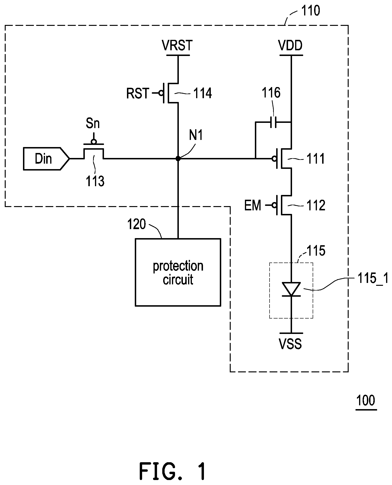
is a schematic diagram of an electronic device according to some embodiments of the disclosure. With reference to , an electronic device 100 includes a pixel circuit 110 and a protection circuit 120 . The pixel circuit 110 includes a driving transistor 111 , a pixel switching transistor 112 , a scan transistor 113 , a reset transistor 114 , a diode element 115 , and a storage capacitor (Cst) 116 . In this embodiment, the first end of the driving transistor 111 is coupled to an operation voltage VDD. The second end of the driving transistor 111 is coupled to the first end of the pixel switching transistor 112 . The control end of the driving transistor 111 is coupled to the first end of the driving transistor 111 and is coupled to the scan transistor 113 , the reset transistor 114 , and the protection circuit 120 through a circuit node N 1 . The second end of the pixel switching transistor 112 is coupled to the first end of the diode element 115 . The control end of the pixel switching transistor 112 may receive a control signal EM. The first end of the scan transistor 113 may receive driving data (or display data) Din. The control end of the scan transistor 113 may receive a scan signal Sn. The second end of the scan transistor 113 is coupled to the control end of the driving transistor 111 through the circuit node N 1 . The first end of the reset transistor 114 is coupled to a reset voltage VRST. The second end of the reset transistor 114 is coupled to the control end of the driving transistor 111 through the circuit node N 1 . The control end of the reset transistor 114 may receive a reset signal RST. The second end of the diode element 115 is coupled to a ground voltage VSS. In some embodiments, the diode element 115 may include a light emitting diode 115 _ 1 . The anode of the light emitting diode 115 _ 1 is coupled to the second end of the pixel switching transistor 112 . The cathode of the light emitting diode 115 _ 1 is coupled to the ground voltage VSS. In some embodiments, the diode element 115 may include multiple light emitting diodes connected in series. The first end of the storage capacitor 116 is coupled to the first end of the driving transistor 111 , and the second end of the storage capacitor 116 is coupled to the control end of the driving transistor 111 .
In this embodiment, the driving transistor 111 , the pixel switching transistor 112 , the scan transistor 113 , and the reset transistor 114 may respectively be P-type thin-film transistors or P-type MOSFETs, but the disclosure is not limited thereto. In addition, in some embodiments, the pixel circuit 110 may further include other transistors and not be limited to the 3T1C pixel circuit architecture shown in . For example, the pixel circuit 110 may be a circuit architecture composed of seven transistors and two capacitors (7T2C) or a circuit architecture composed of eight transistors and two capacitors (8T2C), but the disclosure is not limited thereto. It should be noted that the protection circuit 120 of the disclosure may be applied in various circuit architectures. In some embodiments, the protection circuit 120 and the diode element 115 may be on the same substrate. In some embodiments, the protection circuit 120 and the diode element 115 may be on different substrates.
In this embodiment, the pixel circuit 110 may be respectively operated in a reset mode and a driving mode (which may also be referred to as a display mode or a light emitting mode) during a reset period and a driving period according to the driving data, the control signal EM, the scan signal Sn, and the reset signal RST. In this embodiment, the protection circuit 120 may receive the control signal EM, the scan signal Sn, and the reset signal RST to detect at least one of the scan signal Sn and the reset signal RST. When signal (voltage) abnormality of at least one of the scan signal Sn and the reset signal RST occurs, the protection circuit 120 may provide a shutdown voltage to the control end of the driving transistor 111 through the circuit node N 1 to turn off the driving transistor 111 , which may effectively protect the diode element 115 . In addition, in some embodiments, the protection circuit 120 may further be coupled to other pixel circuits of the electronic device 100 .
is another schematic diagram of an electronic device according to some embodiments of the disclosure. With reference to , an electronic device 200 may include a pixel 210 and a protection circuit 220 . The pixel 210 may include multiple pixel circuits 210 _ 1 to 210 _ 3 , and each of the pixel circuits 210 _ 1 to 210 _ 3 may be respectively implemented as the pixel circuit 110 as described above in the embodiment of , but the number of pixel circuits in the pixel 210 of the disclosure is not limited thereto. In some embodiments, the pixel 210 may include one or multiple pixel circuits. In this embodiment, the pixel circuits 210 _ 1 to 210 _ 3 may, for example, respectively correspond to pixel circuits of red sub-pixels, green sub-pixels, or blue sub-pixels.
In this embodiment, the protection circuit 220 includes a logic circuit 221 , a switching transistor 222 , and connection transistors 223 _ 1 to 223 _ 3 . The connection transistors 223 _ 1 to 223 _ 3 may be respectively coupled to driving transistors in the pixel circuits 210 _ 1 to 210 _ 3 (e.g., the driving transistor 111 in ). The logic circuit 221 is coupled to the first end of the switching transistor 222 . The second end of the switching transistor 222 is coupled to the control end of the connection transistors 223 _ 1 to 223 _ 3 . The control end of the switching transistor 222 may receive the control signal EM. The first ends of the connection transistors 223 _ 1 to 223 _ 3 may receive a protection voltage Vp, and the protection voltage Vp may be the operation voltage VDD shown in , but the disclosure is not limited thereto. The second ends of the connection transistors 223 _ 1 to 223 _ 3 are respectively coupled to the pixel circuits 210 _ 1 to 210 _ 3 . In addition, the logic circuit 221 may receive the control signal EM and at least one of the scan signal and the reset signal (the scan signal Sn and the reset signal RST as shown in ) to detect at least one of the scan signal and the reset signal.
In this embodiment, the switching transistor 222 and the connection transistors 223 _ 1 to 223 _ 3 may respectively be P-type thin-film transistors or P-type MOSFETs, but the disclosure is not limited thereto. In this embodiment, when signal (e.g., a voltage signal or the like) abnormality (e.g., a false trigger or the like) of at least one of the scan signal and the reset signal occurs, the logic circuit 221 may provide a shutdown voltage to the control end of the driving transistors in the pixel circuits 210 _ 1 to 210 _ 3 through the circuit nodes (the circuit node N 1 as shown in ) in the switching transistor 222 , the connection transistors 223 _ 1 to 223 _ 3 , and the pixel circuits 210 _ 1 to 210 _ 3 , so as to turn off the driving transistors in the pixel circuits 210 _ 1 to 210 _ 3 , which may effectively protect the diode elements (the diode element 115 as shown in ) in the pixel circuits 210 _ 1 to 210 _ 3 .
is a circuit diagram of an electronic device according to some embodiments of the disclosure. With reference to , an electronic device 300 may include a pixel 310 and a protection circuit 320 . The pixel 310 may include multiple pixel circuits 310 _ 1 to 310 _ 3 , and each of the pixel circuits 310 _ 1 to 310 _ 3 may be respectively implemented as the pixel circuit 110 as described above in the embodiment of , but the number of pixel circuits in the pixel 310 of the disclosure is not limited thereto. In some embodiments, the pixel 310 may include one or multiple pixel circuits. In this embodiment, the pixel circuits 310 _ 1 to 310 _ 3 may, for example, respectively correspond to pixel circuits of red sub-pixels, green sub-pixels, or blue sub-pixels.
In this embodiment, the protection circuit 320 includes a logic circuit 321 , switching transistors 322 , 324 , connection transistors 323 _ 1 to 323 _ 3 , and impedance circuits 325 , 326 . The connection transistors 323 _ 1 to 323 _ 3 may be respectively coupled to driving transistors in the pixel circuits 310 _ 1 to 310 _ 3 (e.g., the driving transistor 111 in ). The logic circuit 321 is coupled to the first end of the switching transistor 324 . The second end of the switching transistor 324 is coupled to a circuit node N 31 between the first end of the switching transistor 322 and the impedance circuit 325 . The second end of the switching transistor 322 is coupled to the control end of the connection transistors 323 _ 1 to 323 _ 3 and the impedance circuit 326 through a circuit node N 32 . The control end of the switching transistors 322 and 324 may receive the control signal EM. The first ends of the connection transistors 323 _ 1 to 323 _ 3 may receive the protection voltage Vp, and the protection voltage Vp may be the operation voltage VDD shown in , but the disclosure is not limited thereto. The second ends of the connection transistors 323 _ 1 to 323 _ 3 are respectively coupled to the pixel circuits 310 _ 1 to 310 _ 3 .
In this embodiment, the impedance circuit 325 may include transistors 325 _ 1 and 325 _ 2 . The first end of the transistor 325 _ 1 is coupled to the circuit node N 31 . The second end of the transistor 325 _ 1 is coupled to the control end of the transistor 325 _ 1 and the first end of the transistor 325 _ 2 . The second end of the transistor 325 _ 2 is coupled to the control end of the transistor 325 _ 2 and a ground voltage GND. However, in some embodiments, the impedance circuit 325 may also be other types of impedance circuits and not be limited to those shown in .
In this embodiment, the impedance circuit 326 may include a transistor 326 _ 1 . The first end of the transistor 326 _ 1 may receive a reference voltage V 1 , and the reference voltage V 1 is a high potential voltage and may be, for example, the protection voltage Vp. The second end of the transistor 326 _ 1 is coupled to the control end of the transistor 326 _ 1 and the circuit node N 32 . However, in some embodiments, the impedance circuit 326 may also be other types of impedance circuits and not be limited to those shown in .
In this embodiment, the logic circuit 321 includes a circuit connection transistor 321 _ 1 , a switching circuit 321 _ 2 , a circuit switching transistor 321 _ 3 , and an impedance circuit 321 _ 4 . The circuit connection transistor 321 _ 1 is coupled between the switching transistor 324 and the reference voltage V 1 . The first end of the circuit connection transistor 321 _ 1 may receive the reference voltage V 1 . The second end of the circuit connection transistor 321 _ 1 is coupled to the first end of the switching transistor 324 . The switching circuit 321 _ 2 is coupled to the control end of the circuit connection transistor 321 _ 1 . The circuit switching transistor 321 _ 3 is coupled to the reference voltage V 1 . The first end of the circuit switching transistor 321 _ 3 may receive the reference voltage V 1 . The control end of the circuit switching transistor 321 _ 3 may receive the control signal EM. The second end of the circuit switching transistor 321 _ 3 is coupled to the switching circuit 321 _ 2 . The switching circuit 321 _ 2 includes a scan transistor 321 _ 21 and a reset transistor 321 _ 22 . The first end of the scan transistor 321 _ 21 and the reset transistor 321 _ 22 is coupled to the second end of the circuit switching transistor 321 _ 3 . The control end of the scan transistor 321 _ 21 may receive the scan signal Sn. The control end of the reset transistor 321 _ 22 may receive the reset signal RST. The second end of the scan transistor 321 _ 21 and the reset transistor 321 _ 22 is coupled to the impedance circuit 321 _ 4 . The impedance circuit 321 _ 4 may include a transistor 321 _ 41 . The first end of the transistor 321 _ 41 is coupled to the control end of the transistor 321 _ 41 , and is electrically connected with the control end of the circuit connection transistor 321 _ 1 and the second end of the scan transistor 321 _ 21 and the reset transistor 321 _ 22 . The second end of the transistor 321 _ 41 is coupled to the ground voltage GND. However, in some embodiments, the impedance circuit 321 _ 4 may also be other types of impedance circuits and not be limited to those shown in .
In this embodiment, the circuit connection transistor 321 _ 1 , the connection transistors 323 _ 1 to 323 _ 3 , the scan transistor 321 _ 21 , the reset transistor 321 _ 22 , the circuit switching transistor 321 _ 3 , the switching transistors 322 , 324 , and the transistors 321 _ 41 , 325 _ 1 , 325 _ 2 , 326 _ 1 may respectively be P-type thin-film transistors or P-type MOSFETs, but the disclosure is not limited thereto.
Please refer to and together. is a signal timing diagram according to some embodiments of the disclosure. In some embodiments of the disclosure, each of the pixel circuits 310 _ 1 to 310 _ 3 may receive the control signal EM, the reset signal RST, and the scan signal Sn to be operated in a setting mode during a setting period P 1 from time t 0 to time t 5 and be operated in a driving mode during a driving period P 2 from time t 5 to time t 6 according to the control signal EM, the reset signal RST, and the scan signal Sn. With reference to Table 1 below, during the setting period P 1 , the control signal EM is a high potential voltage to turn off the circuit switching transistor 321 _ 3 , the switching transistor 322 , the switching transistor 324 , and the respective pixel switching transistors of the pixel circuits 310 _ 1 to 310 _ 3 .
During a reset period PR from time t 1 to time t 2 , the reset signal RST switches from a high potential voltage to a low potential voltage to turn on the respective reset transistors of the pixel circuits 310 _ 1 to 310 _ 3 and respectively reset the storage capacitors of the pixel circuits 310 _ 1 to 310 _ 3 . During a period PS from time t 3 to time t 4 , the scan signal Sn switches from a high potential voltage to a low potential voltage to turn on the respective scan transistors of the pixel circuits 310 _ 1 to 310 _ 3 and respectively write the driving data into the storage capacitors of the pixel circuits 310 _ 1 to 310 _ 3 . As shown in the operation states 1 to 3 of Table 1 below, the circuit node N 31 maintains a low potential voltage, and the circuit node N 32 maintains a high potential voltage to turn off the connection transistors 323 _ 1 to 323 _ 3 .
During the driving period P 2 between time t 5 and time t 6 , the control signal EM is a low potential voltage to turn on the circuit switching transistor 321 _ 3 , the switching transistor 322 , the switching transistor 324 , and the respective pixel switching transistors of the pixel circuits 310 _ 1 to 310 _ 3 . The reset signal RST and the scan signal Sn are respectively high potential voltages to turn off the respective reset transistors and the scan transistors of the pixel circuits 310 _ 1 to 310 _ 3 . As shown in the operation state 4 of Table 1 below, the circuit nodes N 31 and N 32 are high potential voltage to turn off the connection transistors 323 _ 1 to 323 _ 3 . It should be noted that since the scan transistor 321 _ 21 and the reset transistor 321 _ 22 of the switching circuit 321 _ 2 may also receive the reset signal RST and the scan signal Sn, when signal (voltage) abnormality (a false trigger) of at least one of the reset signal RST and the scan signal Sn occurs, for example, when at least one of the reset signal RST and the scan signal Sn switches from a high potential voltage to a low potential voltage during the driving period P 2 , then at least one of the scan transistor 321 _ 21 and the reset transistor 321 _ 22 is conducted, and the circuit connection transistor 321 _ 1 is thus conducted as well. As shown in the operation states 5 to 7 of Table 1 below, when signal (voltage) abnormality of at least one of the reset signal RST and the scan signal Sn occurs, the circuit nodes N 31 and N 32 may respectively switch to a low potential voltage to conduct the connection transistors 323 _ 1 to 323 _ 3 . In this regard, the circuit connection transistor 321 _ 1 may provide the reference voltage V 1 to the control end of the connection transistors 323 _ 1 to 323 _ 3 through the switching transistors 322 , 324 and the circuit nodes N 31 , N 32 to conduct the connection transistors 323 _ 1 to 323 _ 3 . Next, the connection transistors 323 _ 1 to 323 _ 3 may respectively provide the protection voltage Vp to the respective driving transistors of the pixel circuits 310 _ 1 to 310 _ 3 to turn off the driving transistors. Therefore, the protection circuit 320 may effectively protect the diode elements in the pixel circuits 310 _ 1 to 310 _ 3 of the pixel 310 and may avoid the voltage signal abnormality of at least one of the reset signal RST and the scan signal Sn from causing the damage to the diode elements in the pixel circuits 310 _ 1 to 310 _ 3 , which may thus achieve the current overload protection function of the pixel 310 .
TABLE 1
control signal EM reset signal RST scan signal Sn circuit node N31 circuit node N32
operation state 1 high potential low potential low potential low potential high potential
operation state 2 high potential high potential low potential low potential high potential
operation state 3 high potential low potential high potential low potential high potential
operation state 4 low potential high potential high potential high potential high potential
operation state 5 low potential low potential high potential low potential low potential
operation state 6 low potential high potential low potential low potential low potential
operation state 7 low potential low potential low potential low potential low potential
In addition, in some embodiments, the switching circuit 321 _ 2 may include only one of the scan transistor 321 _ 21 and the reset transistor 321 _ 22 , and when signal (voltage) abnormality of one of the scan signal Sn and the reset signal RST occurs, the protection circuit 320 may conduct the connection transistors 323 _ 1 to 323 _ 3 to turn off the respective driving transistors of the pixel circuits 310 _ 1 to 310 _ 3 , which may thus achieve the current overload protection function of the pixel 310 .
is a circuit diagram of an electronic device according to some embodiments of the disclosure. With reference to , an electronic device 500 may include a pixel 510 and a protection circuit 520 . The pixel 510 may include multiple pixel circuits 510 _ 1 to 510 _ 3 , and each of the pixel circuits 510 _ 1 to 510 _ 3 may be respectively implemented as the pixel circuit 110 as described above in , but the number of pixel circuits in the pixel 510 of the disclosure is not limited thereto. In some embodiments, the pixel 510 may include one or multiple pixel circuits. In this embodiment, the pixel circuits 510 _ 1 to 510 _ 3 may, for example, respectively correspond to pixel circuits of red sub-pixels, green sub-pixels, or blue sub-pixels.
In this embodiment, the protection circuit 520 includes a logic circuit 521 , switching transistors 522 , 524 , connection transistors 523 _ 1 to 523 _ 3 , and impedance circuits 525 , 526 . The connection transistors 523 _ 1 to 523 _ 3 may be respectively coupled to the driving transistors (e.g., the driving transistor 111 in ) in the connection transistors 523 _ 1 to 523 _ 3 . The logic circuit 521 is coupled to the first end of the switching transistor 524 and the first end of the switching transistor 522 through a circuit node N 51 . The second end of the switching transistor 524 is coupled to the impedance circuit 525 . The second end of the switching transistor 522 is coupled to the control end of the connection transistors 523 _ 1 to 523 _ 3 and the impedance circuit 526 through the circuit node N 52 . The control end of the switching transistors 522 and 524 may receive the control signal EM. The first ends of the connection transistors 523 _ 1 to 523 _ 3 may receive the protection voltage Vp, and the protection voltage Vp may be the operation voltage VDD shown in , but the disclosure is not limited thereto. The second ends of the connection transistors 523 _ 1 to 523 _ 3 are respectively coupled to the pixel circuits 510 _ 1 to 510 _ 3 .
In this embodiment, the impedance circuit 525 may include transistors 525 _ 1 and 525 _ 2 . The first end of the transistor 525 _ 1 is coupled to the second end of the switching transistor 524 . The second end of the transistor 525 _ 1 is coupled to the control end of the transistor 525 _ 1 and the first end of the transistor 525 _ 2 . The second end of the transistor 525 _ 2 is coupled to the control end of the transistor 525 _ 2 and the ground voltage GND. However, in some embodiments, the impedance circuit 525 may also be other types of impedance circuits and not be limited to those shown in .
In this embodiment, the impedance circuit 526 may include a transistor 526 _ 1 . The first end of the transistor 526 _ 1 may receive the reference voltage V 1 , and the reference voltage V 1 is a high potential voltage and may be, for example, the protection voltage Vp. The second end of the transistor 526 _ 1 is coupled to the control end of the transistor 526 _ 1 and the circuit node N 52 . However, in some embodiments, the impedance circuit 526 may also be other types of impedance circuits and not be limited to those shown in .
In this embodiment, the logic circuit 521 includes a circuit connection transistor 521 _ 1 , a switching circuit 521 _ 2 , a circuit switching transistor 521 _ 3 , and an impedance circuit 521 _ 4 . The circuit connection transistor 521 _ 1 is coupled between the circuit node N 51 and the reference voltage V 1 . The first end of the circuit connection transistor 521 _ 1 may receive the reference voltage V 1 . The second end of the circuit connection transistor 521 _ 1 is coupled to the first end of the switching transistor 524 . The switching circuit 521 _ 2 is coupled to the control end of the circuit connection transistor 521 _ 1 . The circuit switching transistor 521 _ 3 is coupled to the reference voltage V 1 . The first end of the circuit switching transistor 521 _ 3 may receive the reference voltage V 1 . The control end of the circuit switching transistor 521 _ 3 may receive the control signal EM. The second end of the circuit switching transistor 521 _ 3 is coupled to the switching circuit 521 _ 2 . The switching circuit 521 _ 2 includes a scan transistor 521 _ 21 and a reset transistor 521 _ 22 . The first end of the scan transistor 521 _ 21 and the reset transistor 521 _ 22 is coupled to the second end of the circuit switching transistor 521 _ 3 . The control end of the scan transistor 521 _ 21 may receive the scan signal Sn. The control end of the reset transistor 521 _ 22 may receive the reset signal RST. The second end of the scan transistor 521 _ 21 and the reset transistor 521 _ 22 is coupled to the impedance circuit 521 _ 4 . The impedance circuit 521 _ 4 may include a transistor 521 _ 41 . The first end of the transistor 521 _ 41 is coupled to the control end of the transistor 521 _ 41 , and is electrically connected with the control end of the circuit connection transistor 521 _ 1 and the second end of the scan transistor 521 _ 21 and the reset transistor 521 _ 22 . The second end of the transistor 521 _ 41 is coupled to the ground voltage GND. However, in some embodiments, the impedance circuit 521 _ 4 may also be other types of impedance circuits and not be limited to those shown in .
In this embodiment, the circuit connection transistor 521 _ 1 , the connection transistors 523 _ 1 to 523 _ 3 , the scan transistor 521 _ 21 , the reset transistor 521 _ 22 , the circuit switching transistor 521 _ 3 , the switching transistors 522 , 524 , and the transistors 521 _ 41 , 525 _ 1 , 525 _ 2 , 526 _ 1 may respectively be P-type thin-film transistors or P-type MOSFETs, but the disclosure is not limited thereto.
With reference to and together, the signal timing of may also be applied to an electronic device 500 of . In some embodiments of the disclosure, each of the pixel circuits 510 _ 1 to 510 _ 3 may receive the control signal EM, the reset signal RST, and the scan signal Sn to be operated in a setting mode during the setting period P 1 from time t 0 to time t 5 and be operated in a driving mode during the driving period P 2 from time t 5 to time t 6 according to the control signal EM, the reset signal RST, and the scan signal Sn. With reference to Table 2 below, during the setting period P 1 , the control signal EM is a high potential voltage to turn off the circuit switching transistor 521 _ 3 , the switching transistor 522 , the switching transistor 524 , and the respective pixel switching transistors of the pixel circuits 510 _ 1 to 510 _ 3 .
During the reset period PR from time t 1 to time t 2 , the reset signal RST switches from a high potential voltage to a low potential voltage to turn on the respective reset transistors of the pixel circuits 510 _ 1 to 510 _ 3 and respectively reset the storage capacitors of the pixel circuits 510 _ 1 to 510 _ 3 . During the period PS from time t 3 to time t 4 , the scan signal Sn switches from a high potential voltage to a low potential voltage to turn on the respective scan transistors of the pixel circuits 510 _ 1 to 510 _ 3 and respectively write the driving data into the storage capacitors of the pixel circuits 510 _ 1 to 510 _ 3 . As shown in the operation states 1 to 3 of Table 2 below, the circuit nodes N 51 and N 52 maintain a high potential voltage to turn off the connection transistors 523 _ 1 to 523 _ 3 .
During the driving period P 2 between time t 5 and time t 6 , the control signal EM is a low potential voltage to turn on the circuit switching transistor 521 _ 3 , the switching transistor 522 , the switching transistor 524 , and the respective pixel switching transistors of the pixel circuits 510 _ 1 to 510 _ 3 . The reset signal RST and the scan signal Sn are respectively high potential voltages to turn off the respective reset transistors and the scan transistors of the pixel circuits 510 _ 1 to 510 _ 3 . As shown in the operation state 4 of Table 2 below, the circuit nodes N 51 and N 52 are high potential voltage, so as to turn off the connection transistors 523 _ 1 to 523 _ 3 . It should be noted that since the scan transistor 521 _ 21 and the reset transistor 521 _ 22 of the switching circuit 521 _ 2 may also receive the reset signal RST and the scan signal Sn, when signal (voltage) abnormality (a false trigger) of at least one of the reset signal RST and the scan signal Sn occurs, for example, when at least one of the reset signal RST and the scan signal Sn switches from a high potential voltage to a low potential voltage during the driving period P 2 , then at least one of the scan transistor 521 _ 21 and the reset transistor 521 _ 22 is conducted, and the circuit connection transistor 521 _ 1 is thus conducted as well. As shown in the operation states 5 to 7 of Table 2 below, when signal (voltage) abnormality of at least one of the reset signal RST and the scan signal Sn occurs, the circuit nodes N 51 and N 52 may respectively switch to a low potential voltage to conduct the connection transistors 523 _ 1 to 523 _ 3 . In this regard, the circuit connection transistor 521 _ 1 may provide the reference voltage V 1 to the control end of the connection transistors 523 _ 1 to 523 _ 3 through the switching transistors 522 , 524 and the circuit nodes N 51 , N 52 to conduct the connection transistors 523 _ 1 to 523 _ 3 . Next, the connection transistors 523 _ 1 to 523 _ 3 may respectively provide the protection voltage Vp to the respective driving transistors of the pixel circuits 510 _ 1 to 510 _ 3 to turn off the driving transistors. Therefore, the protection circuit 520 may effectively protect the diode elements in the pixel circuits 510 _ 1 to 510 _ 3 of the pixel 510 and may avoid the voltage signal abnormality of at least one of the reset signal RST and the scan signal Sn from causing the damage to the diode elements in the pixel circuits 510 _ 1 to 510 _ 3 , which may thus achieve the current overload protection function of the pixel 510 .
TABLE 2
control signal EM reset signal RST scan signal Sn circuit node N51 circuit node N52
operation state 1 high potential low potential low potential high potential high potential
operation state 2 high potential high potential low potential high potential high potential
operation state 3 high potential low potential high potential high potential high potential
operation state 4 low potential high potential high potential high potential high potential
operation state 5 low potential low potential high potential low potential low potential
operation state 6 low potential high potential low potential low potential low potential
operation state 7 low potential low potential low potential low potential low potential
In addition, in some embodiments, the switching circuit 521 _ 2 may include only one of the scan transistor 521 _ 21 and the reset transistor 521 _ 22 , and when signal (voltage) abnormality of one of the scan signal Sn and the reset signal RST occurs, the protection circuit 520 may conduct the connection transistors 523 _ 1 to 523 _ 3 to turn off the respective driving transistors of the pixel circuits 510 _ 1 to 510 _ 3 , which may thus achieve the current overload protection function of the pixel 510 .
is a circuit diagram of an electronic device according to a third embodiment of the disclosure. With reference to , an electronic device 600 may include a pixel 610 and a protection circuit 620 . The pixel 610 may include multiple pixel circuits 610 _ 1 to 610 _ 3 , and each of the pixel circuits 610 _ 1 to 610 _ 3 may be respectively implemented as the pixel circuit 110 as described above in , but the number of pixel circuits in the pixel 610 of the disclosure is not limited thereto. In some embodiments, the pixel 610 may include one or multiple pixel circuits. In this embodiment, the pixel circuits 610 _ 1 to 610 _ 3 may, for example, respectively correspond to pixel circuits of red sub-pixels, green sub-pixels, or blue sub-pixels.
In this embodiment, the protection circuit 620 includes a logic circuit 621 , a switching transistor 622 , connection transistors 623 _ 1 to 623 _ 3 , and impedance circuits 625 , 626 . The connection transistors 623 _ 1 to 623 _ 3 may be respectively coupled to the driving transistors (e.g., the driving transistor 111 in ) in the connection transistors 623 _ 1 to 623 _ 3 . The logic circuit 621 is coupled to the first end of the switching transistor 622 and the impedance circuit 625 through a circuit node N 61 . The second end of the switching transistor 622 is coupled to the control end of the connection transistors 623 _ 1 to 623 _ 3 and the impedance circuit 626 through a circuit node N 62 . The control end of the switching transistor 622 may receive the control signal EM. The first ends of the connection transistors 623 _ 1 to 623 _ 3 may receive the protection voltage Vp, and the protection voltage Vp may be the operation voltage VDD shown in , but the disclosure is not limited thereto. The second ends of the connection transistors 623 _ 1 to 623 _ 3 are respectively coupled to the pixel circuits 610 _ 1 to 610 _ 3 .
In this embodiment, the impedance circuit 625 may include transistors 625 _ 1 and 625 _ 2 . The first end of the transistor 625 _ 1 is coupled to the circuit node N 61 . The second end of the transistor 625 _ 1 is coupled to the control end of the transistor 625 _ 1 and the first end of the transistor 625 _ 2 . The second end of the transistor 625 _ 2 is coupled to the control end of the transistor 625 _ 2 and the ground voltage GND. However, in some embodiments, the impedance circuit 625 may also be other types of impedance circuits and not be limited to those shown in .
In this embodiment, the impedance circuit 626 may include a transistor 626 _ 1 . The first end of the transistor 626 _ 1 may receive the reference voltage V 1 , and the reference voltage V 1 is a high potential voltage and may be, for example, the protection voltage Vp. The second end of the transistor 626 _ 1 is coupled to the control end of the transistor 626 _ 1 and the circuit node N 62 . However, in some embodiments, the impedance circuit 626 may also be other types of impedance circuits and not be limited to those shown in .
In this embodiment, the logic circuit 621 includes a circuit connection transistor 621 _ 1 , a switching circuit 621 _ 2 , a circuit switching transistor 621 _ 3 , and an impedance circuit 621 _ 4 . The circuit connection transistor 621 _ 1 is coupled between the circuit node N 61 and the reference voltage V 1 . The first end of the circuit connection transistor 621 _ 1 may receive the reference voltage V 1 . The second end of the circuit connection transistor 621 _ 1 is coupled to the first end of the switching transistor 622 . The switching circuit 621 _ 2 is coupled to the control end of the circuit connection transistor 621 _ 1 . The circuit switching transistor 621 _ 3 is coupled to the reference voltage V 1 . The first end of the circuit switching transistor 621 _ 3 may receive the reference voltage V 1 . The control end of the circuit switching transistor 621 _ 3 may receive the control signal EM. The second end of the circuit switching transistor 621 _ 3 is coupled to the switching circuit 621 _ 2 . The switching circuit 621 _ 2 includes a scan transistor 621 _ 21 and a reset transistor 621 _ 22 . The first end of the scan transistor 621 _ 21 and the reset transistor 621 _ 22 is coupled to the second end of the circuit switching transistor 621 _ 3 . The control end of the scan transistor 621 _ 21 may receive the scan signal Sn. The control end of the reset transistor 621 _ 22 may receive the reset signal RST. The second end of the scan transistor 621 _ 21 and the reset transistor 621 _ 22 is coupled to the impedance circuit 621 _ 4 . The impedance circuit 621 _ 4 may include a transistor 621 _ 41 . The first end of the transistor 621 _ 41 is coupled to the control end of the transistor 621 _ 41 , and is electrically connected with the control end of the circuit connection transistor 621 _ 1 and the second end of the scan transistor 621 _ 21 and the reset transistor 621 _ 22 . The second end of the transistor 621 _ 41 is coupled to the ground voltage GND. However, in some embodiments, the impedance circuit 621 _ 4 may also be other types of impedance circuits and not be limited to those shown in .
In this embodiment, the circuit connection transistor 621 _ 1 , the connection transistors 623 _ 1 to 623 _ 3 , the scan transistor 621 _ 21 , the reset transistor 621 _ 22 , the circuit switching transistor 621 _ 3 , the switching transistor 622 , and the transistors 621 _ 41 , 625 _ 1 , 625 _ 2 , 626 _ 1 may respectively be P-type thin-film transistors or P-type MOSFETs, but the disclosure is not limited thereto.
With reference to and together, the signal timing of may also be applied to an electronic device 600 of . In some embodiments of the disclosure, each of the pixel circuits 610 _ 1 to 610 _ 3 may receive the control signal EM, the reset signal RST, and the scan signal Sn to be operated in a setting mode during the setting period P 1 from time t 0 to time t 5 and be operated in a driving mode during the driving period P 2 from time t 5 to time t 6 according to the control signal EM, the reset signal RST, and the scan signal Sn. With reference to Table 3 below, during the setting period P 1 , the control signal EM is a high potential voltage to turn off the circuit switching transistor 621 _ 3 , the switching transistor 622 , and the respective pixel switching transistors of the pixel circuits 610 _ 1 to 610 _ 3 .
During the reset period PR from time t 1 to time t 2 , the reset signal RST switches from a high potential voltage to a low potential voltage to turn on the respective reset transistors of the pixel circuits 610 _ 1 to 610 _ 3 and respectively reset the storage capacitors of the pixel circuits 610 _ 1 to 610 _ 3 . During the period PS from time t 3 to time t 4 , the scan signal Sn switches from a high potential voltage to a low potential voltage to turn on the respective scan transistors of the pixel circuits 610 _ 1 to 610 _ 3 and respectively write the driving data into the storage capacitors of the pixel circuits 610 _ 1 to 610 _ 3 . As shown in the operation states 2 to 3 of Table 1 below, the circuit node N 61 maintains a low potential voltage, and the circuit node N 62 maintains a high potential voltage to turn off the connection transistors 623 _ 1 to 623 _ 3 .
During the driving period P 2 between time t 5 and time t 6 , the control signal EM is a low potential voltage to turn on the circuit switching transistor 621 _ 3 , the switching transistor 622 , and the respective pixel switching transistors of the pixel circuits 610 _ 1 to 610 _ 3 . The reset signal RST and the scan signal Sn are respectively high potential voltages to turn off the respective reset transistors and the scan transistors of the pixel circuits 610 _ 1 to 610 _ 3 . As shown in the operation state 4 of Table 3 below, the circuit nodes N 61 and N 62 are high potential voltage, so as to turn off the connection transistors 623 _ 1 to 623 _ 3 . It should be noted that since the scan transistor 621 _ 21 and the reset transistor 621 _ 22 of the switching circuit 621 _ 2 may also receive the reset signal RST and the scan signal Sn, when signal (voltage) abnormality (a false trigger) of at least one of the reset signal RST and the scan signal Sn occurs, for example, when at least one of the reset signal RST and the scan signal Sn switches from a high potential voltage to a low potential voltage during the driving period P 2 , then at least one of the scan transistor 621 _ 21 and the reset transistor 621 _ 22 is conducted, and the circuit connection transistor 621 _ 1 is thus conducted as well. As shown in the operation states 5 to 7 of Table 3 below, when signal (voltage) abnormality of at least one of the reset signal RST and the scan signal Sn occurs, the circuit nodes N 61 and N 62 may respectively switch to a low potential voltage to conduct the connection transistors 623 _ 1 to 623 _ 3 . In this regard, the circuit connection transistor 621 _ 1 may provide the reference voltage V 1 to the control end of the connection transistors 623 _ 1 to 623 _ 3 through the switching transistor 622 and the circuit nodes N 61 , N 62 to conduct the connection transistors 623 _ 1 to 623 _ 3 . Next, the connection transistors 623 _ 1 to 623 _ 3 may respectively provide the protection voltage Vp to the respective driving transistors of the pixel circuits 610 _ 1 to 610 _ 3 to turn off the driving transistors. Therefore, the protection circuit 620 may effectively protect the diode elements in the pixel circuits 610 _ 1 to 610 _ 3 of the pixel 610 and may avoid the voltage signal abnormality of at least one of the reset signal RST and the scan signal Sn from causing the damage to the diode elements in the pixel circuits 610 _ 1 to 610 _ 3 , which may thus achieve the current overload protection function of the pixel 610 .
TABLE 3
control signal EM reset signal RST scan signal Sn circuit node N61 circuit node N62
operation state 1 high potential low potential low potential low potential high potential
operation state 2 high potential high potential low potential low potential high potential
operation state 3 high potential low potential high potential low potential high potential
operation state 4 low potential high potential high potential high potential high potential
operation state 5 low potential low potential high potential low potential low potential
operation state 6 low potential high potential low potential low potential low potential
operation state 7 low potential low potential low potential low potential low potential
In addition, in some embodiments, the switching circuit 621 _ 2 may include only one of the scan transistor 621 _ 21 and the reset transistor 621 _ 22 , and when signal (voltage) abnormality of one of the scan signal Sn and the reset signal RST occurs, the protection circuit 620 may conduct the connection transistors 623 _ 1 to 623 _ 3 to turn off the respective driving transistors of the pixel circuits 610 _ 1 to 610 _ 3 , which may thus achieve the current overload protection function of the pixel 610 .
To sum up, the electronic device of the disclosure may self-detect one of the scan signal and the reset signal of the pixel through the protection circuit coupled to the pixel. When abnormality or a false trigger of one of the scan signal and the reset signal of the pixel occurs, the protection circuit may turn off the abnormal pixel, which may reduce the problem of diode element damage in the pixel caused by short circuit or high current.
Finally, it should be noted that: the above embodiments are only used to illustrate technical solutions of the disclosure and are not intended to limit the disclosure. Although the disclosure has been described in detail with reference to the above embodiments, people of ordinary skill in the art should understand that they may still modify the technical solutions described in the above embodiments, or replace some or all of the technical features therein with equivalents, and such modifications or replacements of corresponding technical solutions do not substantially deviate from the scope of the technical solutions of the embodiments of the disclosure.
Figures (6)
Citations
This patent cites (4)
- US10935823
- US20150379956
- US20190312098
- US20200394953