Abstract
A display device includes readout line, first circuit, second circuit, and third circuit. Readout line includes first side and second side. First side is opposite to the second side. Each of first circuit, second circuit, and third circuit is coupled to readout line. Each of first circuit and third circuit is located at first side of readout line. First circuit resets according to first scan signal at first stage. Second circuit is located at second side of readout line. Second circuit and first circuit are arranged in dislocation manner. Second circuit reads first light sensing signal to output to readout line according to first scan signal at first stage. Third circuit and second circuit are arranged in dislocation manner, and third circuit is directly adjacent to first circuit. Third circuit senses light so as to generate second light sensing signal according to second scan signal at first stage.
Claims (20)
1. A display device, comprising: a readout line, comprising a first side and a second side, wherein the first side is opposite to the second side; a first circuit, coupled to the readout line, and located at the first side of the readout line, wherein the first circuit is configured to reset according to a first scan signal at a first stage; a second circuit, coupled to the readout line, and located at the second side of the readout line, wherein the second circuit and the first circuit are arranged in a dislocation manner, wherein the second circuit is configured to read a first light sensing signal of the second circuit so as to output the first scan signal to the readout line according to the first scan signal at the first stage; and a third circuit, coupled to the readout line, and located at the first side of the readout line, wherein the third circuit and the second circuit are arranged in a dislocation manner, wherein the third circuit is directly adjacent to the first circuit, wherein the third circuit is configured to sense a light so as to generate a second light sensing signal according to a second scan signal at the first stage.
11. A display device, comprising: a readout line, comprising a first side and a second side, wherein the first side is opposite to the second side; a first circuit, coupled to the readout line, and located at the first side of the readout line; a second circuit, coupled to the readout line, and located at the second side of the readout line; and a third circuit, coupled to the readout line, and located at the first side of the readout line; wherein each of the first circuit, the second circuit, and the third circuit comprises: an optical sensor, configured to sense a light so as to generate a light sensing signal; a read circuit, coupled to the optical sensor and the readout line, and configured to read the light sensing signal so as to transmit the light sensing signal to the readout line; and a reset circuit, coupled to the read circuit and the optical sensor, and configured to reset the optical sensor; wherein the reset circuit of the first circuit and the read circuit of the second circuit are coupled to a first scan signal line, wherein the reset circuit of the second circuit and the read circuit of the third circuit are coupled to a second scan signal line, wherein the first scan signal line and the second scan signal line are parallel and do not intersect, wherein the reset circuit of the first circuit and the read circuit of the third circuit are directly adjacent to each other.
Show 18 dependent claims
2. The display device of claim 1 , wherein the first circuit, the second circuit, and the third circuit are a same.
3. The display device of claim 2 , wherein the second circuit and the first circuit are not in a same row, and the second circuit and the third circuit are not in a same row.
4. The display device of claim 2 , further comprising: a plurality of pixel rows, perpendicular to the readout line, wherein each of the plurality of pixel rows comprises: a first scan signal line, coupled to the first circuit and the second circuit, wherein the first scan signal line is configured to transmit the first scan signal; and a second scan signal line, coupled to the second circuit and the third circuit, wherein the second scan signal line is configured to transmit the second scan signal.
5. The display device of claim 4 , wherein a phase shift is formed between the first scan signal and the second scan signal.
6. The display device of claim 4 , wherein the first circuit is configured to reset according to the first scan signal at a second stage, wherein the second circuit is configured to reset according to the second scan signal at the second stage, wherein the third circuit is configured to sense a light so as to generate the second light sensing signal according to the second scan signal at the second stage.
7. The display device of claim 6 , wherein the first circuit is configured to sense a light so as to generate the first light sensing signal according to the first scan signal at a third stage, wherein the second circuit is configured to reset according to the second scan signal at the third stage, wherein the third circuit is configured to read the second light sensing signal of the first stage and the second stage according to the second scan signal at the third stage.
8. The display device of claim 7 , wherein the first circuit is configured to sense a light so as to generate a third light sensing signal according to the first scan signal and the second scan signal at a fourth stage, wherein the second circuit is configured to sense a light so as to generate the first light sensing signal according to the first scan signal and the second scan signal at the fourth stage, wherein the third circuit is turned off according to the second scan signal at the fourth stage.
9. The display device of claim 8 , wherein each of the plurality of pixel rows further comprises: a first pixel circuit, coupled to the first scan signal line, and located at the first side of the readout line; and a second pixel circuit, coupled to the second scan signal line, and located at the second side of the readout line.
10. The display device of claim 9 , wherein the display device comprises a first side and a second side, wherein an arrangement sequence from the second side to the first side of the display device is the second pixel circuit, the second circuit, the readout line, the first circuit and the third circuit, and the first pixel circuit.
12. The display device of claim 11 , wherein the second circuit is not in a same row as the first circuit, and the second circuit is not in a same row as the third circuit, wherein the second circuit and the first circuit are arranged in a dislocation manner, and the second circuit and the third circuit are arranged in a dislocation manner.
13. The display device of claim 12 , wherein the display device comprises a first side and a second side, wherein a first arrangement sequence from the first side to the second side of the display device is the optical sensor of the first circuit, the reset circuit of the first circuit and the first scan signal line, the read circuit of the third circuit and the second scan signal line, and the reset circuit and the optical sensor of the third circuit.
14. The display device of claim 13 , wherein a second arrangement sequence from the first side to the second side of the display device is the read circuit of the second circuit, the first scan signal line, the optical sensor and the reset circuit of the second circuit, and the second scan signal line.
15. The display device of claim 14 , wherein the first scan signal line and the second scan signal line are located at a pixel row, wherein the pixel row is perpendicular to the readout line, wherein the pixel row comprises: a first pixel circuit, coupled to the first scan signal line, and located at the first side of the readout line; and a second pixel circuit, coupled to the second scan signal line, and located at the second side of the readout line.
16. The display device of claim 15 , wherein based on a connection between the first side and the second side of the display device, opposite sides of the connection comprise a third side and a fourth side, wherein a third arrangement sequence from the third side to the fourth side of the display device is the second pixel circuit, the second circuit, the readout line, the first circuit and the third circuit, and the first pixel circuit.
17. The display device of claim 11 , wherein the read circuit comprises: a first transistor, comprising a first end, a second end, and a control end, wherein the first end of the first transistor is coupled to the readout line, wherein the control end of the first transistor is coupled to the first scan signal line, and is configured to receive a first scan signal; and a second transistor, comprising a first end, a second end, and a control end, wherein the first end of the second transistor is coupled to the second end of the first transistor, wherein the second end of the second transistor is coupled to a first system high voltage source, wherein the control end of the second transistor is coupled to the reset circuit and the optical sensor.
18. The display device of claim 17 , wherein the reset circuit comprises: a third transistor, comprising a first end, a second end, and a control end, wherein the first end of the third transistor is coupled to the control end of the second transistor of the read circuit and the optical sensor, wherein the second end of the third transistor is coupled to a second system high voltage source, wherein the control end of the third transistor is coupled to the second scan signal line, and is configured to receive a second scan signal.
19. The display device of claim 18 , wherein the optical sensor comprises a first end and a second end, wherein the first end of the optical sensor is coupled to the control end of the second transistor of the read circuit, wherein the second end of the optical sensor is coupled to a system low voltage source.
20. The display device of claim 19 , wherein the optical sensor is located on a different layer from the read circuit and the reset circuit.
Full Description
Show full text →
CROSS-REFERENCE TO RELATED APPLICATION
This application claims priority to Taiwan Application Serial Number 111111738, filed on Mar. 28, 2022, which is herein incorporated by reference in its entirety.
BACKGROUND
Field of Invention
The present disclosure relates to an electronic device. More particularly, the present disclosure relates to a display device in which circuits on both sides of a readout line are arranged in a dislocation manner.
Description of Related Art
Conventional display devices have a large number of readout lines, which reduces a pixel density (or called Pixels Per Inch, PPI) in a panel of a display device and causes readout line area to occupy a certain proportion of a chip bonding of a display device. Therefore, a large number of readout lines is not conducive to designs of various shapes of displays.
For the foregoing reason, there is a need to provide other a circuit structure and a trace design of a display device to solve the problems of the prior art.
SUMMARY
One aspect of the present disclosure provides a display device. The display device includes a readout line, a first circuit, a second circuit, and a third circuit. The readout line includes a first side and a second side. The first side is opposite to the second side. Each of the first circuit, the second circuit, and the third circuit is coupled to the readout line. The first circuit and the third circuit are located at the first side of the readout line. The first circuit is configured to reset according to a first scan signal at a first stage. The second circuit is located at the second side of the readout line. The second circuit and the first circuit are arranged in a dislocation manner. The second circuit is configured to read a first light sensing signal of the second circuit so as to output the first scan signal to the readout line according to the first scan signal at the first stage. The third circuit and the second circuit are arranged in a dislocation manner, and the third circuit is directly adjacent to the first circuit. The third circuit is configured to sense a light so as to generate a second light sensing signal according to a second scan signal at the first stage.
Another aspect of the present disclosure provides a display device. The display device includes a readout line, a first circuit, a second circuit, and a third circuit. The readout line includes a first side and a second side. The first side is opposite to the second side. The first circuit is coupled to the readout line, and is located at the first side of the readout line. The second circuit is coupled to the readout line, and is located at the second side of the readout line. The third circuit is coupled to the readout line, and is located at the first side of the readout line. Each of the first circuit, the second circuit, and the third circuit includes an optical sensor, a read circuit, and a reset circuit. The optical sensor is configured to sense a light so as to generate a light sensing signal. The read circuit is coupled to the optical sensor and the readout line, and is configured to read the light sensing signal so as to transmit the light sensing signal to the readout line. The reset circuit is coupled to the read circuit and the optical sensor, and is configured to reset the optical sensor. The reset circuit of the first circuit and the read circuit of the second circuit are coupled to a first scan signal line. The reset circuit of the second circuit and the read circuit of the third circuit are coupled to a second scan signal line. The first scan signal line and the second scan signal line are parallel and do not intersect. The reset circuit of the first circuit and the read circuit of the third circuit are directly adjacent to each other.
BRIEF DESCRIPTION OF THE DRAWINGS
The present disclosure can be more fully understood by reading the following detailed description of the embodiment, with reference made to the accompanying drawings as follows:
depicts a schematic diagram of a display device according to some embodiments of the present disclosure;
depicts a schematic diagram of a display device according to some embodiments of the present disclosure;
depicts a schematic diagram of a display device according to some embodiments of the present disclosure;
depicts a signal timing diagram of a display device according to some embodiments of the present disclosure;
depicts a state diagram of a display device according to some embodiments of the present disclosure;
depicts a state diagram of a display device according to some embodiments of the present disclosure;
depicts a state diagram of a display device according to some embodiments of the present disclosure;
depicts a state diagram of a display device according to some embodiments of the present disclosure;
depicts a state diagram of a display device according to some embodiments of the present disclosure;
depicts a state diagram of a display device according to some embodiments of the present disclosure;
depicts a state diagram of a display device according to some embodiments of the present disclosure;
depicts a state diagram of a display device according to some embodiments of the present disclosure; and
depicts a state diagram of a display device according to some embodiments of the present disclosure.
DETAILED DESCRIPTION
Reference will now be made in detail to the present embodiments of the invention, examples of which are illustrated in the accompanying drawings. Wherever possible, the same reference numbers are used in the drawings and the description to refer to the same or like parts.
The terminology used herein is for the purpose of describing particular example embodiments only and is not intended to be limiting of the present disclosure. As used herein, the singular forms “a,” “an” and “the” are intended to include the plural forms as well, unless the context clearly indicates otherwise.
Furthermore, it should be understood that the terms, “comprising”, “including”, “having”, “containing”, “involving” and the like, used herein are open-ended, that is, including but not limited to.
The terms used in this specification and claims, unless otherwise stated, generally have their ordinary meanings in the art, within the context of the disclosure, and in the specific context where each term is used. Certain terms that are used to describe the disclosure are discussed below, or elsewhere in the specification, to provide additional guidance to the practitioner skilled in the art regarding the description of the disclosure.
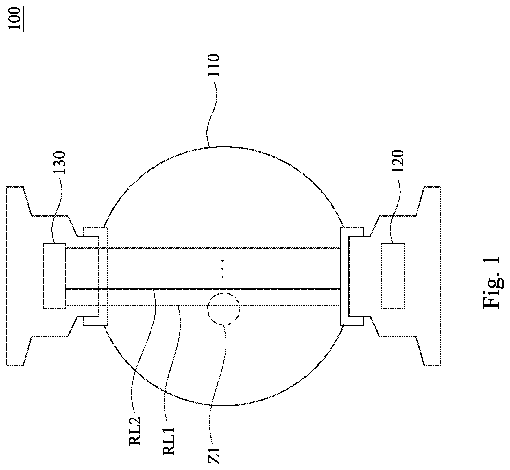
depicts a schematic diagram of a display device 100 according to some embodiments of the present disclosure. In some embodiments, please refer to , the display device 100 includes a display area 110 , a display driver integrated circuit 120 , and a brightness sensing read integrated circuit 130 . The display area 110 includes a plurality of readout lines (e.g.: a readout line RL 1 and a readout line RL 2 ), a plurality of pixel circuits (not shown in the figure), and a plurality of circuits with multiple functions (not shown in the figure). The plurality of circuits with multiple functions will be described in following paragraphs in detail. In some embodiments, the display device 100 can be an electronic watch or an irregularly shaped display.
In some embodiments, the plurality of readout lines (e.g.: a readout line RL 1 and a readout line RL 2 ) are coupled to the brightness sensing read integrated circuit 130 . In some embodiments, after the brightness sensing read integrated circuit 130 and the display driver integrated circuit 120 are integrated into a single integrated circuit, the plurality of readout lines (e.g.: a readout line RL 1 and a readout line RL 2 ) can be coupled to the single integrated circuit.
depicts a schematic diagram of a display device 100 according to some embodiments of the present disclosure. In some embodiments, please refer to and , embodiment of is an enlarged view of a partial region Z 1 on both sides of the readout line RL 1 in .
In some embodiments, please refer to and , the display device 100 includes a readout line RL 1 , a first circuit Sen 1 , a second circuit Sen 2 , and a third circuit Sen 3 .
In some embodiments, please refer to and , the display device 100 further includes a plurality of pixel circuits (e.g.: a plurality of red light pixel circuit R 1 ˜R 4 , a plurality of green light pixel circuit G 1 ˜G 4 , and a plurality of blue light pixel circuit B 1 ˜B 4 ). The embodiments of show pixel rows in two adjacent horizontal rows, a plurality of pixels circuits in two adjacent vertical columns, and the first circuit Sen 1 to the fifth circuit Sen 5 .
Then, the readout line RL 1 includes a first side (e.g.: a right side of the figure) and a second side (e.g.: a left side of the figure). The first side is opposite to the second side. Each of the first circuit Sen 1 , the second circuit Sen 2 , and the third circuit Sen 3 is coupled to the readout line RL 1 . The first circuit Sen 1 and the third circuit Sen 3 are located at the first side of the readout line RL 1 (e.g.: a right side of the figure). The second circuit Sen 2 is located at the second side of the readout line RL 1 (e.g.: a left side of the figure). The second circuit Sen 2 and the first circuit Sen 1 are arranged in a dislocation manner. The third circuit Sen 3 and the second circuit Sen 2 are arranged in a dislocation manner, and the third circuit Sen 3 is directly adjacent to the first circuit Sen 1 .
Furthermore, the first circuit Sen 1 is configured to reset according to a first scan signal S 1 [ n ] at a first stage. The second circuit Sen 2 is configured to read a first light sensing signal of the second circuit Sen 2 so as to output the first scan signal to the readout line RL 1 according to the first scan signal S 1 [ n ] at the first stage. The third circuit Sen 3 is configured to sense a light so as to generate a second light sensing signal according to a second scan signal S 2 [ n ] at the first stage.
It should be noted that the first circuit Sen 1 , the second circuit Sen 2 , and the third circuit Sen 3 are the plurality of circuits with multiple functions in the aforementioned embodiments.
In some embodiments, a circuit structure of the first circuit Sen 1 , second circuit Sen 2 , and third circuit Sen 3 are the same. In some embodiments, the second circuit Sen 2 and the first circuit Sen 1 are not in the same row, and the second circuit Sen 2 and the third circuit Sen 3 are not in the same row.
In some embodiments, please refer to , the first red light pixel circuit R 1 , the first green light pixel circuit G 1 , the first blue light pixel circuit B 1 , the third red light pixel circuit R 3 , the third green light pixel circuit G 3 , the third blue light pixel circuit B 3 are the same pixel column.
Then, the second red light pixel circuit R 2 , the second green light pixel circuit G 2 , the second blue light pixel circuit B 2 , the fourth red light pixel circuit R 4 , the fourth green light pixel circuit G 4 , and the fourth blue light pixel circuit B 4 are the same pixel column.
In some embodiments, please refer to and , the display device 100 includes a first side (e.g.: a right side of the figure) and a second side (e.g.: a left side of the figure). An arrangement sequence from the second side to the first side of the display device 100 is the pixel circuit (e.g.: the first red light pixel circuit R 1 , the first green light pixel circuit G 1 , or the first blue light pixel circuit B 1 ), the second circuit Sen 2 , the readout line RL 1 , the first circuit Sen 1 and the third circuit Sen 3 , and the pixel circuit (e.g.: the second red light pixel circuit R 2 , the second green light pixel circuit G 2 , or the second blue light pixel circuit B 2 ).
In some embodiments, please refer to and , the display device 100 further includes a plurality of pixel rows. The plurality of pixel rows are perpendicular to the readout line RL 1 . Pixel rows above the figure include a first scan signal line L 1 and second scan signal line L 2 . Pixel rows below the figure include a secondary first scan signal line L 3 and a secondary second scan signal line L 4 .
Then, the first scan signal line L 1 is coupled to the first circuit Sen 1 and the second circuit Sen 2 . The second scan signal line L 2 is coupled to the second circuit Sen 2 and the third circuit Sen 3 .
In some embodiments, the first scan signal line L 1 is configured to transmit the first scan signal S 1 [ n ]. The second scan signal line L 2 is configured to transmit the second scan signal S 2 [ n].
Furthermore, the first scan signal line L 1 , the second scan signal line L 2 , the first red light pixel circuit R 1 , the first green light pixel circuit G 1 , the first blue light pixel circuit B 1 , the second red light pixel circuit R 2 , the second green light pixel circuit G 2 , the second blue light pixel circuit B 2 , the second circuit Sen 2 are the same pixel row. The first circuit Sen 1 and the third circuit Sen 3 are partially overlapped with the pixel row above the figure.
Similarly, the secondary first scan signal line L 3 is coupled to the third circuit Sen 3 and a fourth circuit Sen 4 . The secondary second scan signal line L 4 is coupled to the fourth circuit Sen 4 and the fifth circuit Sen 5 .
Then, the secondary first scan signal line L 3 is configured to transmit a secondary first scan signal S 1 [ n+ 1]. The secondary second scan signal line L 4 is configured to transmit a secondary second scan signal S 2 [ n+ 1].
Furthermore, the secondary first scan signal line L 3 , the secondary second scan signal line L 4 , the third red light pixel circuit R 3 , the third green light pixel circuit G 3 , the third blue light pixel circuit B 3 , the fourth red light pixel circuit R 4 , the fourth green light pixel circuit G 4 and the fourth blue light pixel circuit B 4 , and the fourth circuit Sen 4 are the same pixel row. The third circuit Sen 3 and the fifth circuit Sen 5 are partially overlapped with the pixel row below the figure.
depicts a schematic diagram of a display device 100 according to some embodiments of the present disclosure. In some embodiments, please refer to and , The embodiment of is a schematic diagram of a detailed circuit structure of the first circuit Sen 1 to the fifth circuit Sen 5 of .
In some embodiments, a circuit structure of each of the first circuit Sen 1 to the fifth circuit Sen 5 is the same. It should be noted that parts of circuit structure of the first circuit Sen 1 and the fifth circuit Sen 5 are not shown in the figure. In practice, a circuit structure of each of first circuit Sen 1 and the fifth circuit Sen 5 is the same as a circuit structure of the third circuit Sen 3 .
In some embodiments, each of the first circuit Sen 1 to the fifth circuit Sen 5 includes three transistors and an optical sensor.
Because the circuit structures of the first circuit Sen 1 to the fifth circuit Sen 5 are the same, in some embodiments, the first circuit Sen 1 includes a first transistor T 1 , an optical sensor SRO 1 and two transistors (not shown in the figure). Please start form a top end and a right end of each of an element shown in the figure as a first end, the optical sensor SRO 1 includes a first end and a second end. The first end of the optical sensor SRO 1 is coupled to a system low voltage source SVSS.
Then, the first transistor T 1 includes a first end, a second end, and a control end. The first end of the first transistor T 1 is coupled to the second end of the optical sensor SRO 1 . The second end of the first transistor T 1 is coupled to a second system high voltage source SVDD 2 . The control end of the first transistor T 1 is coupled to the first scan signal line L 1 , and is configured to receive the first scan signal S 1 [ n].
In some embodiments, the second circuit Sen 2 includes a second transistor T 2 , a third transistor T 3 , a fourth transistor T 4 , and an optical sensor SRO 2 .
In some embodiments, the second transistor T 2 includes a first end, a second end, and a control end. The first end of the second transistor T 2 is coupled to the readout line RL 1 . The control end of the second transistor T 2 is coupled to the first scan signal line L 1 , and is configured to receive the first scan signal S 1 [ n].
In some embodiments, the third transistor T 3 includes a first end, a second end, and a control end. The first end of the third transistor T 3 is coupled to the second end of the second transistor T 2 . The second end of the third transistor T 3 is coupled to a first system high voltage source SVDD 1 . The control end of the third transistor T 3 is coupled to the optical sensor SRO 2 .
In some embodiments, the fourth transistor T 4 includes a first end, a second end, and a control end. The first end of the fourth transistor T 4 is couple to the control end of the third transistor T 3 and the optical sensor SRO 2 . The second end of the fourth transistor T 4 is coupled to the second system high voltage source SVDD 2 . The control end of the fourth transistor T 4 is coupled to second scan signal line L 2 , and is configured to receive the second scan signal S 2 [ n].
In some embodiments, the optical sensor SRO 2 includes a first end and a second end. The first end of the optical sensor SRO 2 is coupled to the control end of the third transistor T 3 . The second end of the optical sensor SRO 2 is coupled to the system low voltage source SVSS.
In some embodiments, the third circuit Sen 3 includes a fifth transistor T 5 , a sixth transistor T 6 , a seventh transistor T 7 , and an optical sensor SRO 3 . A circuit structure of the third circuit Sen 3 is similar to a circuit structure of the second circuit Sen 2 , and repetitious details are omitted herein.
In some embodiments, the fourth circuit Sen 4 includes an eighth transistor T 8 , a ninth transistor T 9 , a tenth transistor T 10 , and an optical sensor SRO 4 . A circuit structure of the fourth circuit Sen 4 is similar to a circuit structure of the second circuit Sen 2 , and repetitious details are omitted herein.
In some embodiments, the fifth circuit Sen 5 includes an eleventh transistor T 11 , a twelfth transistor T 12 , a transistor (not shown in the figure) and an optical sensor (not shown in the figure).
In some embodiments, in order to facilitate the understanding of an operation of the display device of , please refer to to . depicts a signal timing diagram of a display device according to some embodiments of the present disclosure. Each of to depicts a state diagram of a display device according to some embodiments of the present disclosure.
In some embodiments, please refer to , , and , at a first stage I 1 , the first scan signal S 1 [ n ] is at a low voltage level. Each of the second scan signal S 2 [ n ], the secondary first scan signal S 1 [ n+ 1], and the secondary second scan signal S 2 [ n+ 1] is at a high voltage level. The first transistor T 1 of the first circuit Sen 1 is turned on in response to the first scan signal S 1 [ n ] so that the second system high voltage source SVDD 2 resets the optical sensor SRO 1 . At the same time, the second transistor T 2 of the second circuit Sen 2 is turned on in response to the first scan signal S 1 [ n ] so as to read a first light sensing signal of the second circuit Sen 2 to output the first light sensing signal to the readout line RL 1 . Each of the optical sensor SRO 3 of the third circuit Sen 3 , the optical sensor SRO 4 of the fourth circuit Sen 4 , and the optical sensor SRO 5 of the fifth circuit Sen 5 is configured to sense a light. In some embodiments, the first light sensing signal is stored in the optical sensor SRO 2 of the second circuit Sen 2 .
At this time, the first circuit Sen 1 is configured to reset the optical sensor the optical sensor SRO 1 . The second circuit Sen 2 is configured to read first light sensing signal. Each of the third circuit Sen 3 to the fifth circuit Sen 5 is configured to sense a light. Please refer to again, at this time, states of the pixel circuits on both sides of the readout line RL 1 (e.g.: pixel circuits R 1 ˜B 1 and pixel circuits R 2 ˜B 2 ) are that the pixel circuits are turned off after driving the pixels.
It should be noted that the pixel circuits on both sides of the readout line RL 1 (e.g.: pixel circuits R 1 ˜B 1 and pixel circuits R 2 ˜B 2 ), and the first circuit Sen 1 to the third circuit Sen 3 share the first scan signal line L 1 and the second scan signal line L 2 .
In some embodiments, please refer to , , and , at a second stage I 2 , Each of the first scan signal S 1 [ n ] and the second scan signal S 2 [ n ] is at a low voltage level. Each of the secondary first scan signal S 1 [ n+ 1] and the secondary second scan signal S 2 [ n+ 1] is at a high voltage level. The first transistor T 1 of the first circuit Sen 1 is turned on in response to the first scan signal S 1 [ n ] so that the second system high voltage source SVDD 2 resets the optical sensor SRO 1 . The fourth transistor T 4 of the second circuit Sen 2 is turned on in response to the second scan signal S 2 [ n ] so that the second system high voltage source SVDD 2 resets the optical sensor SRO 2 and turns off the third transistor T 3 to stop reading first light sensing signal. The fifth transistor T 5 of the third circuit Sen 3 is turned on in response to the second scan signal S 2 [ n ]. Each of the optical sensor SRO 3 of the third circuit Sen 3 , the optical sensor SRO 4 of the fourth circuit Sen 4 , and the optical sensor SRO 5 of the fifth circuit Sen 5 is configured to sense a light.
At this time, first circuit Sen 1 is configured to reset the optical sensor SRO 1 . The second circuit Sen 2 is configured to reset the optical sensor SRO 2 and turn off the third transistor T 3 . Each of the third circuit Sen 3 to the fifth circuit Sen 5 is configured to sense a light. Please refer to again, at this time, states of the pixel circuits on both sides of the readout line RL 1 (e.g.: pixel circuits R 1 ˜B 1 and pixel circuits R 2 ˜B 2 ) are that the pixel circuits are reset.
In some embodiments, please refer to , , and , at a third stage I 3 , the second scan signal S 2 [ n ] is at a low voltage level. Each of the first scan signal S 1 [ n ], the secondary first scan signal S 1 [ n+ 1], and the secondary second scan signal S 2 [ n+ 1] is at a high voltage level. The fourth transistor T 4 of the second circuit Sen 2 is turned on in response to the second scan signal S 2 [ n ] so that the second system high voltage source SVDD 2 resets the optical sensor SRO 2 . The fifth transistor T 5 of the third circuit Sen 3 is turned on in response to the second scan signal S 2 [ n ] so as to read the second light sensing signal of the third circuit Sen 3 . In some embodiments, the second light sensing signal is stored in the optical sensor SRO 3 of the third circuit Sen 3 . Each of the optical sensor SRO 1 of the first circuit Sen 1 , the optical sensor SRO 4 of the fourth circuit Sen 4 and the optical sensor SRO 5 of the fifth circuit Sen 5 is configured to sense a light.
At this time, the first circuit Sen 1 is configured to sense a light. The second circuit Sen 2 is configured to reset the optical sensor SRO 2 . The third circuit Sen 3 is configured to read the second light sensing signal of the third circuit Sen 3 . Each of the fourth circuit Sen 4 to the fifth circuit Sen 5 is configured to sense a light. Please refer to again, at this time, states of the pixel circuits on both sides of the readout line RL 1 (e.g.: pixel circuits R 1 ˜B 1 and pixel circuits R 2 ˜B 2 ) are that the pixel circuits are compensated.
In some embodiments, please refer to , , and , at a fourth stage I 4 , each of the first scan signal S 1 [ n ], the second scan signal S 2 [ n ], the secondary first scan signal S 1 [ n+ 1], and the secondary second scan signal S 2 [ n+ 1] is at a high voltage level. Each of the first transistor T 1 of the first circuit Sen 1 , the second transistor T 2 and the fourth transistor T 4 of the second circuit Sen 2 , the fifth transistor T 5 and the seventh transistor T 7 of the third circuit Sen 3 , the eighth transistor T 8 and the tenth transistor T 10 of the fourth circuit Sen 4 , and the eleventh transistor T 11 of the fifth circuit Sen 5 are turned off.
At this time, each of the first circuit Sen 1 and the second circuit Sen 2 is configured to sense a light. The third circuit Sen 3 is in a hold state. The fourth circuit Sen 4 and the fifth circuit Sen 5 are configured to sense a light. Please refer to again, at this time, states of the pixel circuits on both sides of the readout line RL 1 (e.g.: pixel circuits R 1 ˜B 1 and pixel circuits R 2 ˜B 2 ) are that the pixel circuits are in a hold state.
In some embodiments, please refer to , , and , at a fifth stage I 5 , the secondary first scan signal S 1 [ n+ 1] is at a low voltage level. Each of the first scan signal S 1 [ n ], the second scan signal S 2 [ n ], and the secondary second scan signal S 2 [ n+ 1] is at a high voltage level. The seventh transistor T 7 of the third circuit Sen 3 is turned on in response to the secondary first scan signal S 1 [ n+ 1] so that the second system high voltage source SVDD 2 resets the optical sensor SRO 3 of the third circuit Sen 3 and turns off the sixth transistor T 6 so as to stop reading the second light sensing signal. The eighth transistor T 8 of the fourth circuit Sen 4 is turned on in response to the secondary first scan signal S 1 [ n+ 1] so as to read a light sensing signal of the fourth circuit Sen 4 .
At this time, the first circuit Sen 1 and the second circuit Sen 2 is configured to sense a light. The third circuit Sen 3 is configured to switch from the hold state to a reset state. The fourth circuit Sen 4 is configured to read the light sensing signal to readout line RL 1 . The fifth circuit Sen 5 is configured to sense a light.
Please refer to again, at this time, states of the pixel circuits of an upper pixel row on both sides of the readout line RL 1 (e.g.: pixel circuits R 1 ˜B 1 and pixel circuits R 2 ˜B 2 ) are that the pixel circuits are in a hold state. The pixel circuits of a lower pixel row on both sides of the readout line RL 1 (e.g.: pixel circuits R 3 ˜B 3 and pixel circuits R 4 ˜B 4 ) are switched from driving pixel state to be in a hold state.
In some embodiments, please refer to , , and , at a sixth stage I 6 , each of the secondary first scan signal S 1 [ n+ 1] and the secondary second scan signal S 2 [ n+ 1] is at a low voltage level. Each of the first scan signal S 1 [ n ] and the second scan signal S 2 [ n ] is at a high voltage level. The seventh transistor T 7 of the third circuit Sen 3 is turned on in response to the secondary first scan signal S 1 [ n+ 1] so that the second system high voltage source SVDD 2 resets the optical sensor SRO 3 and turns off the sixth transistor T 6 . The tenth transistor T 10 of the fourth circuit Sen 4 is turned on in response to the secondary second scan signal S 2 [ n+ 1] so that the second system high voltage source SVDD 2 resets the optical sensor SRO 4 and turns off the ninth transistor T 9 so as to stop reading the light sensing signal.
At this time, each of the first circuit Sen 1 and the second circuit Sen 2 is configured to sense a light. The third circuit Sen 3 is configured to reset. The fourth circuit Sen 4 is configured to switch from a reading state to a reset state. The fifth circuit Sen 5 is configured to sense a light.
Please refer to again, at this time, states of the pixel circuits of an upper pixel row on both sides of the readout line RL 1 (e.g.: pixel circuits R 1 ˜B 1 and pixel circuits R 2 ˜B 2 ) are that the pixel circuits are in a hold state. The pixel circuits of a lower pixel row on both sides of the readout line RL 1 (e.g.: pixel circuits R 3 ˜B 3 and pixel circuits R 4 ˜B 4 ) are configured to reset.
In some embodiments, please refer to , , and , at a seventh stage I 7 , the secondary second scan signal S 2 [ n+ 1] is at a low voltage level. Each of the first scan signal S 1 [ n ], the second scan signal S 2 [ n ], and the secondary first scan signal S 1 [ n+ 1] is at a high voltage level. The tenth transistor T 10 of the fourth circuit Sen 4 is turned on in response to the secondary second scan signal S 2 [ n+ 1] so that the second system high voltage source SVDD 2 resets the optical sensor SRO 4 . The eleventh transistor T 11 of the fifth circuit Sen 5 is turned on in response to the secondary second scan signal S 2 [ n+ 1] so as to read the light sensing signal of the fifth circuit Sen 5 .
At this time, Each of the first circuit Sen 1 , the second circuit Sen 2 , and the third circuit Sen 3 is configured to sense a light. The fourth circuit Sen 4 is configured to reset. The fifth circuit Sen 5 is configured to read the light sensing signal.
Please refer to again, at this time, states of the pixel circuits of an upper pixel row on both sides of the readout line RL 1 (e.g.: pixel circuits R 1 ˜B 1 and pixel circuits R 2 ˜B 2 ) are that the pixel circuits are in a hold state. The pixel circuits of a lower pixel row on both sides of the readout line RL 1 (e.g.: pixel circuits R 3 ˜B 3 and pixel circuits R 4 ˜B 4 ) are compensated.
In some embodiments, please refer to , , and , at an eighth stage I 8 , each of the first scan signal S 1 [ n ], the second scan signal S 2 [ n ], the secondary first scan signal S 1 [ n+ 1], and the secondary second scan signal S 2 [ n+ 1] is at a high voltage level. Each of the first transistor T 1 of the first circuit Sen 1 , the second transistor T 2 and the fourth transistor T 4 of the second circuit Sen 2 , the fifth transistor T 5 and the seventh transistor of the third circuit Sen 3 , the eighth transistor T 8 and the tenth transistor T 10 of fourth circuit Sen 4 , and the eleventh transistor T 11 of the fifth circuit Sen 5 is turned off.
At this time, each of the first circuit Sen 1 to the fifth circuit Sen 5 is configured to sense a light. Please refer to again, states of the pixel circuits of an upper pixel row on both sides of the readout line RL 1 (e.g.: pixel circuits R 1 ˜B 1 and pixel circuits R 2 ˜B 2 ) are that the pixel circuits are configured to drive pixels. The pixel circuits of a lower pixel row on both sides of the readout line RL 1 (e.g.: pixel circuits R 3 ˜B 3 and pixel circuits R 4 ˜B 4 ) are in a hold state.
depicts a state diagram of a display device according to some embodiments of the present disclosure.
In some embodiments, please refer to , the display device includes a readout line RL 1 , a first circuit Sen 1 , a second circuit Sen 2 , and a third circuit Sen 3 . The readout line RL 1 includes a first side (e.g.: a right side of the figure) and a second side (e.g.: a left side of the figure). The first side is opposite to the second side. The first circuit Sen 1 is coupled to the readout line RL 1 , and is located at the first side of the readout line RL 1 (e.g.: a right side of the figure). The second circuit Sen 2 is coupled to the readout line RL 1 , and is located at the second side of the readout line RL 1 (e.g.: a left side of the figure). The third circuit Sen 3 is coupled to the readout line RL 1 , and is located at the first side of the readout line RL 1 (e.g.: a right side of the figure). Each of the first circuit Sen 1 , the second circuit Sen 2 , and the third circuit Sen 3 includes an optical sensor (e.g.: an optical sensor SRO 1 , an optical sensor SRO 2 , and an optical sensor SRO 3 ), a read circuit (e.g.: a read circuit Sen 21 and a read circuit Sen 31 ), and a reset circuit (e.g.: a reset circuit Sen 12 , a reset circuit Sen 22 , and a reset circuit Sen 32 ).
In some embodiments, please refer to and , the display device 100 includes a first side (e.g.: a top side of the figure) and a second side (e.g.: a bottom side of the figure). A first arrangement sequence from the first side to the second side of the display device 100 of is the optical sensor SRO 1 of the first circuit Sen 1 , the reset circuit Sen 12 of the first circuit Sen 1 and the first scan signal line L 1 , the read circuit Sen 31 of the third circuit Sen 3 and the second scan signal line L 2 , and the reset circuit Sen 32 and the optical sensor SRO 3 of the third circuit Sen 3 . A second arrangement sequence from the first side to the second side of the display device 100 of is the read circuit Sen 21 of the second circuit Sen 2 , the first scan signal line L 1 , the optical sensor SRO 2 and the reset circuit Sen 22 of the second circuit Sen 2 , and the second scan signal line L 2 .
Then, please refer to , based on a connection between the first side and the second side of the display device 100 of , opposite sides of the connection comprise a third side (e.g.: a left side of the figure) and a fourth side (e.g.: a right side of the figure). A third arrangement sequence from the third side to the fourth side of the display device is the pixel circuit (e.g.: the red light pixel circuit R 1 , the green light pixel circuit G 1 , or the blue light pixel circuit B 1 ), the second circuit Sen 2 , the readout line RL 1 , the first circuit Sen 1 and the third circuit Sen 3 , and the pixel circuit (e.g.: the red light pixel circuit R 2 , the green light pixel circuit G 2 , or the blue light pixel circuit B 2 ).
Then, the optical sensor (e.g.: the optical sensor SRO 2 ) is configured to sense a light to generate a light sensing signal. the read circuit (e.g.: the read circuit Sen 21 ) is coupled to the optical sensor (e.g.: the optical sensor SRO 2 ) and the readout line RL 1 , and is configured to read the light sensing signal so as to transmit the light sensing signal to the readout line RL 1 . The reset circuit (e.g.: the reset circuit Sen 22 ) is coupled to the read circuit (e.g.: the read circuit Sen 21 ) and the optical sensor (e.g.: the optical sensor SRO 2 ), and is configured to reset the optical sensor (e.g.: the optical sensor SRO 2 ). The reset circuit Sen 12 of the first circuit Sen 1 and the read circuit Sen 21 of the second circuit Sen 2 are coupled to a first scan signal line L 1 . The reset circuit Sen 22 of the second circuit Sen 2 and the read circuit Sen 31 of the third circuit Sen 3 are coupled to a second scan signal line L 2 . The first scan signal line L 1 and the second scan signal line L 2 are parallel and do not intersect. The reset circuit Sen 12 of the first circuit Sen 1 and the read circuit Sen 31 of the third circuit Sen 3 are directly adjacent to each other. It should be noted that a difference between embodiments of and aforementioned embodiments is that circuits on both sides of the readout line are further divided into more detailed circuit structures. A rest of the circuit structures and operations of embodiments of are similar to the embodiments of to , and repetitious details are omitted herein.
In some embodiments, please refer to to , each of the optical sensor SRO 1 to the optical sensor SRO 5 is located on a different layer of the display device from the first circuit Sen 1 to the fifth circuit Sen 5 .
Based on the above embodiments, the present disclosure provides a display device to reduce a number of readout lines of a display device, and make the same pixel row can perform circuit operations of reading, resetting and light sensing at the same time, so that a circuit structure of a display device of the present disclosure can be designed for displays of various shapes.
Although the present disclosure has been described in considerable detail with reference to certain embodiments thereof, other embodiments are possible. Therefore, the spirit and scope of the appended claims should not be limited to the description of the embodiments contained herein.
It will be apparent to those skilled in the art that various modifications and variations can be made to the structure of the present disclosure without departing from the scope or spirit of the present disclosure. In view of the foregoing, it is intended that the present disclosure cover modifications and variations of the present disclosure provided they fall within the scope of the following claims.
Figures (13)
Citations
This patent cites (8)
- US20080084377
- US20110018850
- US20130257833
- US20200192170
- US20200192544
- US20200393300
- US103365486
- US2007011233