Abstract
A method for driving a display device includes operating an input sensing part in a direct sensing mode. The input sensing part includes first sensing electrodes connected to transmission lines and second sensing electrodes connected to the sensing lines. The input sensing part operates in a noise sensing mode and proximity sensing mode when a call mode is performed. The proximity sensing mode includes generation of a proximity sensing signal concerning proximity of a user to the display device. Noise sensed in the noise sensing mode is removed from the proximity sensing signal when the proximity sensing signal indicates the user is proximate. At least one of a voltage level of a drive signal, a number of simultaneous transmission lines to which the drive signal is simultaneously applied, or a frequency of the drive signal is differently set in the noise sensing mode as compared to the proximity sensing mode.
Claims (19)
1. A method for driving a display device, the method comprising: operating an input sensing part in a direct sensing mode, the input sensing part including a plurality of first sensing electrodes connected to a plurality of transmission lines and a plurality of second sensing electrodes connected to a plurality of sensing lines; operating the input sensing part in a noise sensing mode and a proximity sensing mode when a call mode is performed based on a user being engaged in a telephone call, the proximity sensing mode including generation of a proximity sensing signal concerning a proximity of the user to the display device; and removing noise sensed in the noise sensing mode from the proximity sensing signal when the proximity sensing signal indicates a proximity state of the user, wherein at least one of a voltage level of a drive signal applied to the plurality of transmission lines, a number of simultaneous transmission lines to which the drive signal is simultaneously applied, or a frequency of the drive signal is differently set in the noise sensing mode as compared to the proximity sensing mode, and wherein the input sensing part generates an electric field in the noise sensing mode having a magnitude that is less than a magnitude of an electric field generated by the input sensing part in the proximity sensing mode.
12. A method for driving a display device, the method comprising: operating an input sensing part in a direct sensing mode, the input sensing part including a plurality of first sensing electrodes connected to a plurality of transmission lines and a plurality of second sensing electrodes connected to a plurality of sensing lines; operating the input sensing part in the direct sensing mode and a first proximity sensing mode, when a call mode is performed, the first proximity sensing mode is performed a first number of times; and operating the input sensing part in a second proximity sensing mode when a direct touch of a user is sensed or a proximity state of the user is sensed, the second proximity sensing mode is performed a second number of times that is different from the first number of times of the first proximity sensing mode, wherein when the direct touch of the user is sensed, the second number of times that the second proximity sensing mode is performed is less than the first number of times that the first proximity sensing mode is performed.
Show 17 dependent claims
2. The method of claim 1 , wherein the voltage level of the drive signal in the noise sensing mode is less than the voltage level of the drive signal in the proximity sensing mode.
3. The method of claim 1 , wherein the number of simultaneous transmission lines in the noise sensing mode is less than the number of simultaneous transmission lines in the proximity sensing mode.
4. The method of claim 1 , wherein the frequency of the drive signal in the noise sensing mode is greater than the frequency of the drive signal in the proximity sensing mode.
5. The method of claim 1 , wherein in the noise sensing mode, the electric field is applied to a display panel positioned under the input sensing part and is not applied to the user above the input sensing part.
6. The method of claim 5 , wherein the operating of the input sensing part in the noise sensing mode includes sensing noise of the input sensing part caused by the display panel.
7. The method of claim 1 , wherein: the voltage level of the drive signal in the noise sensing mode is less than the voltage level of the drive signal in the proximity sensing mode; and the number of simultaneous transmission lines in the noise sensing mode is less than the number of simultaneous transmission lines in the proximity sensing mode.
8. The method of claim 1 , wherein: the voltage level of the drive signal in the noise sensing mode is less than the voltage level of the drive signal in the proximity sensing mode; and the frequency of the drive signal in the noise sensing mode is greater than the frequency of the drive signal in the proximity sensing mode.
9. The method of claim 1 , wherein: the number of simultaneous transmission lines in the noise sensing mode is less than the number of simultaneous transmission lines in the proximity sensing mode; and the frequency of the drive signal in the noise sensing mode is greater than the frequency of the drive signal in the proximity sensing mode.
10. The method of claim 1 , wherein: the voltage level of the drive signal in the noise sensing mode is less than the voltage level of the drive signal in the proximity sensing mode; the number of simultaneous transmission lines in the noise sensing mode is less than the number of simultaneous transmission lines in the proximity sensing mode; and the frequency of the drive signal in the noise sensing mode is greater than the frequency of the drive signal in the proximity sensing mode.
11. The method of claim 1 , wherein: the proximity sensing mode and the noise sensing mode are each performed a plurality of times; and a number of times that the proximity sensing mode is performed is larger than a number of times that the noise sensing mode is performed.
13. The method of claim 12 , wherein in each frame, the first proximity sensing mode is performed between two adjacent performances of the direct sensing mode.
14. The method of claim 12 , wherein when the proximity state of the user is sensed, the second number of times that the second proximity sensing mode is performed is greater than the first number of times that the first proximity sensing mode is performed.
15. The method of claim 14 , wherein when the proximity state of the user is sensed, in each frame, the second number of times that the second proximity sensing mode is performed is greater than a number of times that the direct sensing mode is performed.
16. The method of claim 14 , wherein when the proximity state of the user is sensed the second number of times that the second proximity sensing mode is performed gradually increases.
17. The method of claim 12 , wherein: when the direct touch of the user is sensed, a period of the second proximity sensing mode is greater than a period of the first proximity sensing mode; and when the proximity state of the user is sensed, the period of the second proximity sensing modes is less than the period of the first proximity sensing modes.
18. The method of claim 12 , wherein at least one of a voltage level of a drive signal applied to the plurality of transmission lines, a number of simultaneous transmission lines to which the drive signal is simultaneously applied, or a frequency of the drive signal is differently set in the direct sensing mode as compared to the first and second proximity sensing modes.
19. The method of claim 18 , wherein: the voltage level of the drive signal in the first and second proximity sensing modes is greater than the voltage level of the drive signal in the direct sensing mode; the number of simultaneous transmission lines in the first and second proximity sensing modes is greater than the number of simultaneous transmission lines in the direct sensing mode; and the frequency of the drive signal in the first and second proximity sensing modes is less than the frequency of the drive signal in the direct sensing mode.
Full Description
Show full text →
CROSS-REFERENCE TO RELATED APPLICATIONS
This application claims priority under 35 U.S.C. § 119 to Korean Patent Application No. 10-2021-0125956, filed on Sep. 23, 2021 in the Korean Intellectual Property Office, the disclosure of which is incorporated by reference in its entirety herein.
1. TECHNICAL FIELD
Embodiments of the present disclosure described herein relate to a method for driving a display device.
2. DISCUSSION OF RELATED ART
Various types of electronic devices include a display device for displaying an image, such as a smart phone, a digital camera, a notebook computer, a navigation device, a smart television, and the like. The display device includes a display panel for generating an image, an input device such as an input sensing part, a camera for taking an external image, and various sensors.
The input sensing part is disposed on the display panel and senses a touch of a user. The camera generates and stores an image of an external object. The sensors may include a fingerprint sensor, a proximity sensor, and/or an illuminance sensor.
The fingerprint sensor senses a fingerprint on the display panel. The proximity sensor senses an object adjacent to the display device. The proximity sensor includes a light emitting part that generates and outputs light (e.g., infrared light) and a light receiving part that senses the light reflected from an object. The illuminance sensor senses luminance around the display device. The fingerprint sensor, the proximity sensor, and the illuminance sensor may be manufactured as separate modules and are disposed in the display device.
SUMMARY
Embodiments of the present disclosure provide a driving method of a display device for increasing the sensitivity of proximity sensing through an input sensing part in a call mode and easily performing a direct sensing mode and a proximity sensing mode in the call mode.
According to an embodiment of the present disclosure, a method for driving a display device includes operating an input sensing part in a direct sensing mode. The input sensing part includes a plurality of first sensing electrodes connected to a plurality of transmission lines and a plurality of second sensing electrodes connected to a plurality of sensing lines. The input sensing part is operated in a noise sensing mode and a proximity sensing mode when a call mode is performed. The proximity sensing mode includes generation of a proximity sensing signal concerning a proximity of a user to the display device. Noise sensed in the noise sensing mode is removed from the proximity sensing signal when the proximity sensing signal indicates a proximity state of the user. At least one of a voltage level of a drive signal applied to the plurality of transmission lines, a number of simultaneous transmission lines to which the drive signal is simultaneously applied, or a frequency of the drive signal is differently set in the noise sensing mode as compared to the proximity sensing mode.
According to an embodiment of the present disclosure, a method for driving a display device includes operating an input sensing part in a direct sensing mode. The input sensing part includes a plurality of first sensing electrodes connected to a plurality of transmission lines and a plurality of second sensing electrodes connected to a plurality of sensing lines. The input sensing part is operated in the direct sensing mode and a first proximity sensing mode, when a call mode is performed. The first proximity sensing mode is performed a first number of times. The input sensing part is operated in a second proximity sensing mode when a direct touch of a user is sensed or a proximity state of the user is sensed. The second proximity sensing mode is performed a second number of times that is different from the first number of times of the first proximity sensing mode.
BRIEF DESCRIPTION OF THE DRAWINGS
The above and other objects and features of the present disclosure will become apparent by describing in detail embodiments thereof with reference to the accompanying drawings.
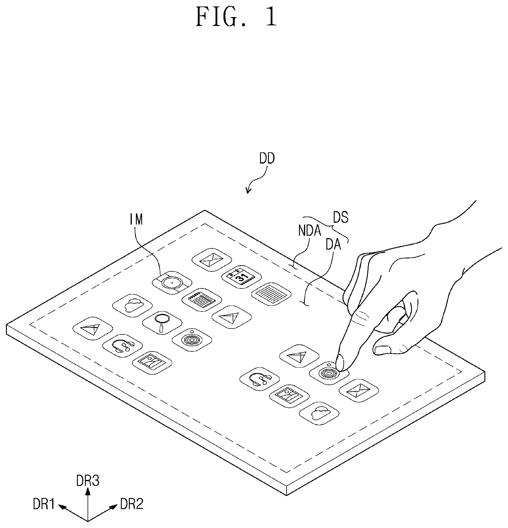
is a perspective view of a display device according to an embodiment of the present disclosure.
is a cross-sectional view of the display device illustrated in according to an embodiment of the present disclosure.
is a cross-sectional view of a display panel illustrated in according to an embodiment of the present disclosure.
is a plan view of the display panel illustrated in according to an embodiment of the present disclosure.
is a plan view of an input sensing part illustrated in according to an embodiment of the present disclosure.
is an enlarged plan view of two adjacent first sensing parts and two adjacent second sensing parts illustrated in according to an embodiment of the present disclosure.
is a enlarged plan view illustrating only first and second detectors and an extending pattern in according to an embodiment of the present disclosure.
is an enlarged plan view illustrating only a connecting pattern in according to an embodiment of the present disclosure.
is a cross-sectional view of an input sensing part taken along line I-I′ illustrated in according to an embodiment of the present disclosure.
is a cross-sectional view of an input sensing part taken along line II-II′ illustrated in according to an embodiment of the present disclosure.
A and 11 B are plan views for explaining operation of the input sensing part illustrated in according to embodiments of the present disclosure;
is a flowchart illustrating a method for driving the display device according to an embodiment of the present disclosure.
is a side view illustrating the display panel, the input sensing part, and a proximity state of a user in a call mode of according to an embodiment of the present disclosure.
to 16 are diagrams illustrating timings of noise sensing and proximity sensing and states of a drive signal according to embodiments of the present disclosure.
to 20 are diagrams illustrating states of a drive signal according to embodiments of the present disclosure.
is a diagram illustrating timing of noise sensing and proximity sensing according to an embodiment of the present disclosure.
is a flowchart illustrating a method for driving the display device according to an embodiment of the present disclosure.
is a diagram illustrating timing of a direct sensing mode of a first mode and timing of a direct sensing mode and a first proximity sensing mode of a second mode illustrated in according to embodiments of the present disclosure.
is a diagram illustrating timing of a direct sensing mode and a second proximity sensing mode of the second mode when a direct touch illustrated in is sensed according to an embodiment of the present disclosure.
to 27 are diagrams illustrating various timings of the direct sensing mode and the second proximity sensing mode of the second mode when a proximity state illustrated in is sensed according to embodiments of the present disclosure.
is a side view illustrating a state of a drive signal applied to the input sensing part in the first and second proximity sensing modes illustrated in to 27 according to an embodiment of the present disclosure.
is a side view illustrating a state of a drive signal applied to the input sensing part in the direct sensing modes illustrated in to 27 according to an embodiment of the present disclosure.
DETAILED DESCRIPTION OF EMBODIMENTS
In this specification, when it is mentioned that a component (or, an area, a layer, a part, etc.) is referred to as being “on”, “connected to” or “coupled to” another component, this means that the component may be directly on, connected to, or coupled to the other component or a third component may be present therebetween. When a component (or, an area, a layer, a part, etc.) is referred to as being “directly on”, “directly connected to” or “directly coupled to” another component, a third component is not present therebetween.
Identical reference numerals refer to identical components. Additionally, in the drawings, the thicknesses, proportions, and dimensions of components are exaggerated for effective description.
As used herein, the term “and/or” includes all of one or more combinations defined by related components.
Terms such as first, second, and the like may be used to describe various components, but the components should not be limited by the terms. The terms may be used only for distinguishing one component from other components. For example, without departing the scope of the present disclosure, a first component may be referred to as a second component, and similarly, the second component may also be referred to as the first component. The terms of a singular form may include plural forms unless otherwise specified.
In addition, terms such as “below”, “under”, “above”, and “over” are used to describe a relationship of components illustrated in the drawings. The terms are relative concepts and are described based on directions illustrated in the drawing.
Unless otherwise defined, all terms used herein, including technical or scientific terms, have the same meanings as those generally understood by those skilled in the art to which the present disclosure pertains. Such terms as those defined in a generally used dictionary are to be interpreted as having meanings equal to the contextual meanings in the relevant field of art, and are not to be interpreted as having ideal or excessively formal meanings unless clearly defined as having such in the present application.
It should be understood that terms such as “comprise”, “include”, and “have”, when used herein, specify the presence of stated features, numbers, steps, operations, components, parts, or combinations thereof, but do not preclude the presence or addition of one or more other features, numbers, steps, operations, components, parts, or combinations thereof.
Hereinafter, embodiments of the present disclosure will be described with reference to the accompanying drawings.
is a perspective view of a display device according to an embodiment of the present disclosure.
Referring to , the display device DD according to an embodiment of the present disclosure may have a rectangular shape with relatively long sides extending in a first direction DR 1 and relatively short sides extending in a second direction DR 2 crossing the first direction DR 1 . However, embodiments of the present disclosure are not necessarily limited thereto. In an embodiment, the display device DD may have various shapes such as a circular shape, a polygonal shape, and the like.
Hereinafter, a direction substantially vertically crossing a plane defined by the first direction DR 1 and the second direction DR 2 is defined as a third direction DR 3 . As used herein, the expression “when viewed on the plane” may mean that it is viewed in the third direction DR 3 .
In an embodiment, an upper surface of the display device DD may be defined as a display surface DS and may have a plane defined by the first direction DR 1 and the second direction DR 2 . Images IM generated by the display device DD may be provided to a user through the display surface DS. For example, in the embodiment of , the images IM are software application icons. However embodiments of the present disclosure are not necessarily limited thereto and the images IM may be various different subject matter.
The display surface DS may include a display area DA and a non-display area NDA around the display area DA. The display area DA may display an image, and the non-display area NDA may not display an image. The non-display area NDA may surround the display area DA and may define the border of the display device DD printed in a predetermined color. For example, in an embodiment, the non-display area NDA may completely surround the display area DA (e.g., in the first and second directions DR 1 , DR 2 ). However, embodiments of the present disclosure are not necessarily limited thereto and the non-display area NDA may not surround the display area DA on at least one side in some embodiments.
The display device DD may be used in large electronic devices such as a television, a monitor, and outdoor signage. In addition, the display device DD may be used in small and medium-sized electronic devices such as a personal computer, a notebook computer, a personal digital terminal, a car navigation device, a game machine, a smart phone, a tablet computer, and a camera. However, these electronic devices are merely illustrative, and the display device DD may be used in other electronic devices without departing from the spirit and scope of the present disclosure.
is a cross-sectional view of the display device illustrated in .
In , a cross-section of the display device DD viewed in the first direction DR 1 is illustrated.
Referring to , in an embodiment, the display device DD may include a display panel DP, an input sensing part ISP, an anti-reflection layer RPL, a window WIN, a panel protection film PPF, and first to third adhesive layers AL 1 , AL 2 , and AL 3 .
In an embodiment, the display panel DP may be a flexible display panel. In an embodiment, the display panel DP may be an emissive display panel. However, embodiments of the present disclosure are not necessarily limited thereto. For example, the display panel DP may be an organic light emitting display panel or an inorganic light emitting display panel. An emissive layer of the organic light emitting display panel may contain an organic light emitting material. An emissive layer of the inorganic light emitting display panel may contain quantum dots, quantum rods, and the like. Hereinafter, it will be exemplified that the display panel DP is an organic light emitting display panel for convenience of explanation.
The input sensing part ISP may be disposed over the display panel DP (e.g., in the third direction DR 3 ). The input sensing part ISP may include a plurality of sensors for sensing an external input in a capacitive manner. In an embodiment, the input sensing part ISP may be directly manufactured on the display panel DP when the display device DD is manufactured. However, embodiments of the present disclosure are not necessarily limited thereto. For example, in an embodiment, the input sensing part ISP may be manufactured as a panel separate from the display panel DP and may be attached to the display panel DP by an adhesive layer.
The anti-reflection layer RPL may be disposed over the input sensing part ISP (e.g., in the third direction DR 3 ). The anti-reflection layer RPL may be a film for preventing reflection of external light. The anti-reflection layer RPL may decrease the reflectivity of external light incident toward the display panel DP from above the display device DD.
When external light travelling toward the display panel DP is reflected from the display panel DP and provided back to the user, the user may visually recognize the external light as in a mirror. To prevent such a phenomenon, the anti-reflection layer RPL may include a plurality of color filters that display the same colors as pixels of the display panel DP.
In an embodiment, external light may be filtered in the same colors as those of the pixels by the color filters. In this embodiment, the external light may not be visible to the user. In an embodiment, the anti-reflection layer RPL may include a phase retarder and/or a polarizer to decrease the reflectivity of external light. However, embodiments of the present disclosure are not necessarily limited thereto.
The window WIN may be disposed over the anti-reflection layer RPL (e.g., in the third direction DR 3 ). The window WIN may protect the display panel DP, the input sensing part ISP, and the anti-reflection layer RPL from external scratches and external shocks.
The panel protection film PPF may be disposed under the display panel DP (e.g., in the third direction DR 3 ). The panel protection film PPF may protect a lower portion of the display panel DP. In an embodiment, the panel protection film PPF may contain a flexible plastic material such as polyethylene terephthalate (PET). However, embodiments of the present disclosure are not necessarily limited thereto.
The first adhesive layer AL 1 may be disposed between the display panel DP and the panel protection film PPF (e.g., in the third direction DR 3 ), and the display panel DP and the panel protection film PPF may be bonded to each other by the first adhesive layer AL 1 . The second adhesive layer AL 2 may be disposed between the anti-reflection layer RPL and the input sensing part ISP (e.g., in the third direction DR 3 ), and the anti-reflection layer RPL and the input sensing part ISP may be bonded to each other by the second adhesive layer AL 2 . The third adhesive layer AL 3 may be disposed between the window WIN and the anti-reflection layer RPL (e.g., in the third direction DR 3 ), and the window WIN and the anti-reflection layer RPL may be bonded to each other by the third adhesive layer AL 3 .
is a cross-sectional view of the display panel illustrated in .
In , a cross-section of the display panel DP viewed in the first direction DR 1 is illustrated.
Referring to , the display panel DP may include a substrate SUB, a circuit element layer DP-CL disposed on the substrate SUB, a display element layer DP-OLED disposed on the circuit element layer DP-CL, and a thin-film encapsulation layer TFE disposed on the display element layer DP-OLED.
The substrate SUB may include a display area DA and a non-display area NDA around the display area DA. In an embodiment, the substrate SUB may contain a flexible plastic material such as glass or polyimide (P 1 ). The display element layer DP-OLED may be disposed in the display area DA.
A plurality of pixels may be disposed in the circuit element layer DP-CL and the display element layer DP-OLED. Each of the pixels may include a transistor disposed in the circuit element layer DP-CL and a light emitting element disposed in the display element layer DP-OLED and connected to the transistor. A configuration of the pixel will be described below in detail.
The thin-film encapsulation layer TFE may be disposed on the circuit element layer DP-CL to cover the display element layer DP-OLED. The thin-film encapsulation layer TFE may protect the pixels from moisture, oxygen, and external foreign matter.
is a plan view of the display panel illustrated in .
Referring to , the display device DD may include the display panel DP, a scan driver SDV, a data driver DDV, an light emission driver EDV, and a plurality of first pads PD 1 .
The display panel DP may have a rectangular shape with relatively long sides extending in the first direction DR 1 and relatively short sides extending in the second direction DR 2 . However, the shape of the display panel DP is not limited thereto. The display panel DP may include a display area DA and a non-display area NDA surrounding the display area DA.
The display panel DP may include a plurality of pixels PX, a plurality of scan lines SL 1 to SLm, a plurality of data lines DL 1 to DLn, a plurality of light emission lines EL 1 to ELm, first and second control lines CSL 1 and CSL 2 , first and second power lines PL 1 and PL 2 , and connecting lines CNL. “in” and “n” are natural numbers.
The pixels PX may be disposed in the display area DA. The scan driver SDV and the light emission driver EDV may be disposed on left and right sides (e.g., in the second direction DR 2 ) of the non-display area NDA adjacent to the relatively long sides of the display panel DP, respectively. The data driver DDV may be disposed in the non-display area NDA adjacent to one of the relatively short sides of the display panel DP. For example, as shown in , in an embodiment, when viewed on the plane, the data driver DDV may be adjacent to a lower end of the display panel DP (e.g., in the first direction DR 1 ). However, embodiments of the present disclosure are not necessarily limited thereto.
The scan lines SL 1 to SLm may extend in the second direction DR 2 and may be connected to the pixels PX and the scan driver SDV. The data lines DL 1 to DLn may extend in the first direction DR 1 and may be connected to the pixels PX and the data driver DDV. The light emission lines EL 1 to ELm may extend in the second direction DR 2 and may be connected to the pixels PX and the light emission driver EDV.
The first power line PL 1 may extend in the first direction DR 1 and may be disposed in the non-display area NDA. The first power line PL 1 may be disposed between the display area DA and the light emission driver EDV (e.g., in the second direction DR 2 ). However, embodiments of the present disclosure are not necessarily limited thereto. For example, the first power line PL 1 may be disposed between the display area DA and the scan driver SDV (e.g., in the second direction DR 2 ).
The connecting lines CNL may extend in the second direction DR 2 and may be arranged in the first direction DR 1 and connected to the first power line PL 1 and the pixels PX. A first voltage may be applied to the pixels PX through the first power line PL 1 and the connecting lines CNL connected with each other.
The second power line PL 2 may be disposed in the non-display area NDA and may extend along the relatively long sides of the display panel DP and the other relatively short side of the display panel DP where the data driver DDV is not disposed. In an embodiment, the second power line PL 2 may be disposed outward of the scan driver SDV and the light emission driver EDV (e.g., in the second direction DR 2 ).
In an embodiment, the second power line PL 2 may extend toward the display area DA and may be connected to the pixels PX. A second voltage having a lower level than the first voltage may be applied to the pixels PX through the second power line PL 2 .
The first control line CSL 1 may be connected to the scan driver SDV and may extend toward the lower end of the display panel DP. The second control line CSL 2 may be connected to the light emission driver EDV and may extend toward the lower end of the display panel DP. The data driver DDV may be disposed between the first control line CSL 1 and the second control line CSL 2 .
The first pads PD 1 may be disposed in the non-display area NDA adjacent to the lower end of the display panel DP (e.g., in the first direction DR 1 ) and may be closer to the lower end of the display panel DP than the data driver DDV. The data driver DDV, the first power line PL 1 , the second power line PL 2 , the first control line CSL 1 , and the second control line CSL 2 may be connected to the first pads PD 1 . The data lines DL 1 to DLn may be connected to the data driver DDV, and the data driver DDV may be connected to the first pads PDs corresponding to the data lines DL 1 to DLn.
In an embodiment, the display device DD may further include a timing controller for controlling operations of the scan driver SDV, the data driver DDV, and the light emission driver EDV and a voltage generator for generating the first and second voltages. The timing controller and the voltage generator may be connected to the corresponding first pads PD 1 through a printed circuit board.
The scan driver SDV may generate a plurality of scan signals, and the scan signals may be applied to the pixels PX through the scan lines SL 1 to SLm. The data driver DDV may generate a plurality of data voltages, and the data voltages may be applied to the pixels PX through the data lines DL 1 to DLn. The light emission driver EDV may generate a plurality of light emission signals, and the light emission signals may be applied to the pixels PX through the light emission lines EL 1 to ELm.
The pixels PX may receive the data voltages in response to the scan signals. The pixels PX may display an image by emitting light having luminance corresponding to the data voltages in response to the light emission signals.
is a plan view of the input sensing part illustrated in .
Referring to , the input sensing part ISP may include a plurality of sensing electrodes, such as first sensing electrodes SE 1 and second sensing electrodes SE 2 , a plurality of lines TX 1 to TXh and RX 1 to RXk, and a plurality of second and third pads PD 2 and PD 3 . The sensing electrodes, the lines TX 1 to TXh and RX 1 to RXk, and the second and third pads PD 2 and PD 3 may be disposed on the thin-film encapsulation layer TFE (e.g., in the third direction DR 3 ).
A planar area of the input sensing part ISP may include an active area AA and a non-active area NAA around the active area AA (e.g., in the first direction DR 1 and/or the second direction DR 2 ). The active area AA may overlap the display area DA, and the non-active area NAA may overlap the non-display area NDA.
The sensing electrodes, such as the first and second sensing electrodes SE 1 and SE 2 may be disposed in the active area AA, and the second and third pads PD 2 and PD 3 may be disposed in the non-active area NAA. The second pads PD 2 and the third pads PD 3 may be adjacent to a lower end (e.g., in the first direction DR 1 ) of the input sensing part ISP when viewed on the plane. The first pads PD 1 may be disposed between the second pads PD 2 and the third pads PD 3 (e.g., in the second direction DR 2 ) when viewed on the plane.
The lines TX 1 to TXh and RX 1 to RXk may be connected to ends of the sensing electrodes, such as the first and second sensing electrodes SE 1 and SE 2 , may extend to the non-active area NAA, and may be connected to the second and third pads PD 2 and PD 3 . In an embodiment, a sensing controller for controlling the input sensing part ISP may be connected to the second and third pads PD 2 and PD 3 through a printed circuit board.
In an embodiment, the first sensing electrodes SE 1 may extend in the first direction DR 1 and are arranged in the second direction DR 2 . The plurality of second sensing electrodes SE 2 may extend in the second direction DR 2 and are arranged in the first direction DR 1 . The second sensing electrodes SE 2 may be insulated from the first sensing electrodes SE 1 and may extend to cross the first sensing electrodes SE 1 .
The lines TX 1 to TXh and RX 1 to RXk may include the plurality of first lines TX 1 to TXh connected to the first sensing electrodes SE 1 and the plurality of second lines RX 1 to RXk connected to the second sensing electrodes SE 2 . “h” and “k” are natural numbers. The first lines TX 1 to TXh may extend to the non-active area NAA and may be connected to the second pads PD 2 . The second lines RX 1 to RXk may extend to the non-active area NAA and may be connected to the third pads PD 3 .
The first lines TX 1 to TXh, when viewed on the plane, may be disposed in the non-active area NAA adjacent to the lower side of the active area AA (e.g., in the first direction DR 1 ). The second lines RX 1 to RXk, when viewed on the plane, may be disposed in the non-active area NAA adjacent to the right side of the active area AA (e.g., in the second direction DR 2 ). The first lines TX 1 to TXh may be defined as transmission lines, and the second lines RX 1 to RXk may be defined as sensing lines.
Each of the first sensing electrodes SE 1 may include a plurality of first sensing parts SP 1 arranged in the first direction DR 1 and a plurality of connecting patterns CP connecting the first sensing parts SP 1 . Each of the connecting patterns CP may be disposed between two first sensing parts SP 1 adjacent to each other in the first direction DR 1 and may connect the two first sensing parts SP 1 .
Each of the second sensing electrodes SE 2 may include a plurality of second sensing parts SP 2 arranged in the second direction DR 2 and a plurality of extending patterns EP extending from the second sensing parts SP 2 . Each of the extending patterns EP may be disposed between two second sensing parts SP 2 adjacent to each other in the second direction DR 2 and may extend from the two second sensing parts SP 2 .
The first sensing parts SP 1 and the second sensing parts SP 1 may be spaced apart from each other without overlapping each other and may be alternately disposed. Capacitance may be formed by the first sensing parts SP 1 and the second sensing parts SP 2 . The extending patterns EP may not overlap the connecting patterns CP.
In an embodiment, the first and second sensing electrodes SE 1 and SE 2 may be formed of silver, gold, copper, aluminum, platinum, palladium, chromium, titanium, tungsten, niobium, tantalum, vanadium, iron, manganese, cobalt, nickel, zinc, tin, molybdenum, or an alloy thereof. However, embodiments of the present disclosure are not necessarily limited thereto.
is an enlarged view of two adjacent first sensing parts and two adjacent second sensing parts illustrated in . is a view illustrating only first and second detectors and an extending pattern in . is a view illustrating only a connecting pattern in .
Referring to , 7 , and 8 , the first sensing parts SP 1 and the second sensing parts SP 2 may have a mesh shape. To have a mesh shape, each of the first and second sensing parts SP 1 and SP 2 may include a plurality of first branches BP 1 extending in a first diagonal direction DDR 1 and a plurality of second branches BP 2 extending in a second diagonal direction DDR 2 .
As shown in , in an embodiment, the first diagonal direction DDR 1 may be a direction crossing the first and second directions DR 1 and DR 2 on the plane defined by the first and second directions DR 1 and DR 2 . The second diagonal direction DDR 2 may be defined as a direction crossing the first diagonal direction DDR 1 on the plane defined by the first and second directions DR 1 and DR 2 . For example, the first direction DR 1 and the second direction DR 2 may cross each other at a right angle, and the first diagonal direction DDR 1 and the second diagonal direction DDR 2 may cross each other at a right angle. However, embodiments of the present disclosure are not necessarily limited thereto.
The first branches BP 1 and the second branches BP 2 of each of the first and second sensing parts SP 1 and SP 2 may cross each other and may be integrally formed with each other. Touch openings TOP having a rhombic shape may be defined by the first branches BP 1 and the second branches BP 2 .
The area on the plane of each of the pixels PX illustrated in may include an emissive area EA and a non-emissive area NEA around the emissive area EA. The non-emissive area NEA may be disposed between the emissive areas EA. A light emitting element of each of the above-described pixels PX may be disposed in the emissive area EA. Light generated from the light emitting elements may be output through the emissive areas EA. When viewed on the plane, the emissive areas EA may be disposed in the touch openings TOP, respectively.
The first and second sensing parts SP 1 and SP 2 may be disposed in the non-emissive area NEA. As the first and second sensing parts SP 1 and SP 2 are disposed in the non-emissive area EA, light generated from the light emitting elements may be normally output without being affected by the first and second sensing parts SP 1 and SP 2 .
The connecting pattern CP may extend so as not to overlap the extending pattern EP and may connect the first sensing parts SP 1 . The connecting pattern CP may be connected to the first sensing parts SP 1 through a plurality of contact holes TC-CH. The structure of the contact holes TC-CH will be described below with reference to . The connecting pattern CP may extend toward the first sensing parts SP 1 through areas overlapping the second sensing parts SP 2 .
The extending pattern EP may be disposed between the first sensing parts SP 1 (e.g., in the first direction DR 1 ) and may extend from the second sensing parts SP 2 . The second sensing parts SP 2 and the extending pattern EP may be integrally formed with each other. In an embodiment, the extending pattern EP may have a mesh shape. In an embodiment, the extending pattern EP, the first sensing parts SP 1 , and the second sensing parts P 2 may be disposed in the same layer and may be formed by being simultaneously subjected to patterning with the same material.
The connecting pattern CP may include a first extension EX 1 and a second extension EX 2 having a shape symmetric to the first extension EX 1 . The extending pattern EP may be disposed between the first extension EX 1 and the second extension EX 2 . The first extension EX 1 may extend through an area overlapping one of the second sensing parts SP 2 and may be connected to the first sensing parts SP 1 . The second extension EX 2 may extend through an area overlapping the other one of the second sensing parts SP 2 and may be connected to the first sensing parts SP 1 .
Hereinafter, the first sensing parts SP 1 are defined as the upper first sensing part SP 1 and the lower first sensing part SP 1 depending on the relative positions thereof. Furthermore, the second sensing parts SP 2 are defined as the left second sensing part SP 2 and the right second sensing part SP 2 depending on the relative positions thereof.
In an embodiment, predetermined portions of the first and second extensions EX 1 and EX 2 adjacent to one side of the first and second extensions EX 1 and EX 2 may be connected to the lower first sensing part SP 1 through the plurality of contact holes TC-CH. Predetermined portions of the first and second extensions EX 1 and EX 2 adjacent to an opposite side of the first and second extensions EX 1 and EX 2 may be connected to the upper first sensing part SP 1 through the plurality of contact holes TC-CH.
The first extension EX 1 may include a first sub-extension EX 1 _ 1 and a second sub-extension EX 1 _ 2 extending in the first diagonal direction DDR 1 , a third sub-extension EX 1 _ 3 and a fourth sub-extension EX 1 _ 4 extending in the second diagonal direction DDR 2 , a first sub-conductive pattern SCP 1 extending in the second diagonal direction DDR 2 , and a second sub-conductive pattern SCP 2 extending in the first diagonal direction DDR 1 .
In an embodiment, predetermined portions of the first and second sub-extensions EX 1 _ 1 and EX 1 _ 2 adjacent to one side of the first and second sub-extensions EX 1 _ 1 and EX 1 _ 2 may be connected to the lower first sensing part SP 1 through the plurality of contact holes TC-CH. Predetermined portions of the third and fourth sub-extensions EX 1 _ 3 and EX 1 _ 4 adjacent to one side of the third and fourth sub-extensions EX 1 _ 3 and EX 1 _ 4 may be connected to the upper first sensing part SP 1 through the plurality of contact holes TC-CH.
An opposite side of the first sub-extension EX 1 _ 1 may extend from an opposite side of the third sub-extension EX 1 _ 3 , and an opposite side of the second sub-extension EX 1 _ 2 may extend from an opposite side of the fourth sub-extension EX 1 _ 4 . The first sub-conductive pattern SCP 1 may extend from the opposite side of the fourth sub-extension EX 1 _ 4 in the second diagonal direction DDR 2 and may extend to the first sub-extension EX 1 _ 1 . The second sub-conductive pattern SCP 2 may extend from the opposite side of the second sub-extension EX 1 _ 2 in the first diagonal direction DDR 1 and may extend to the third sub-extension EX 1 _ 3 .
In an embodiment, the first sub-extension EX 1 _ 1 , the second sub-extension EX 1 _ 2 , the third sub-extension EX 1 _ 3 , the fourth sub-extension EX 1 _ 4 , the first sub-conductive pattern SCP 1 , and the second sub-conductive pattern SCP 2 may be integrally formed.
The first and second sub-extensions EX 1 _ 1 and EX 1 _ 2 may extend to cross a predetermined number of second branches BP 2 adjacent to the lower first sensing part SP 1 among the second branches BP 2 of the right second sensing part SP 2 . The first branches BP 1 of the right second sensing part SP 2 may not be disposed in a partial area that overlaps the first and second sub-extensions EX 1 _ 1 and EX 1 _ 2 and the second sub-conductive pattern SCP 2 .
The third and fourth sub-extensions EX 1 _ 3 and EX 1 _ 4 may extend to cross a predetermined number of first branches BP 1 adjacent to the upper first sensing part SP 1 among the first branches BP 1 of the right second sensing part SP 2 . The second branches BP 2 of the right second sensing part SP 2 may not be disposed in a partial area that overlaps the third and fourth sub-extensions EX 1 _ 3 and EX 1 _ 4 and the first sub-conductive pattern SCP 1 .
The second extension EX 2 may include a fifth sub-extension EX 2 _ 1 and a sixth sub-extension EX 2 _ 2 extending in the second diagonal direction DDR 2 , a seventh sub-extension EX 2 _ 3 and an eighth sub-extension EX 2 _ 4 extending in the first diagonal direction DDR 1 , a third sub-conductive pattern SCP 3 extending in the first diagonal direction DDR 1 , and a fourth sub-conductive pattern SCP 4 extending in the second diagonal direction DDR 2 .
The left second sensing part SP 2 may have a structure symmetric to the right second sensing part SP 2 , and the second extension EX 2 may have a structure symmetric to the first extension EX 1 . Accordingly, descriptions of the fifth to eighth sub-extensions EX 2 _I to EX 2 _ 4 and the third and fourth sub-conductive patterns SCP 3 and SCP 4 will hereinafter be omitted for convenience of explanation.
is a cross-sectional view taken along line I-I′ illustrated in . Referring to , an insulating layer IOL may be disposed on the thin-film encapsulation layer TFE. The insulating layer IOL may include an inorganic insulating layer. At least one insulating layer IOL may be provided on the thin-film encapsulation layer TFE. For example, two inorganic insulating layers IOL may be sequentially stacked on the thin-film encapsulation layer TFE.
The connecting pattern CP may be disposed on the insulating layer IOL (e.g., directly thereon in the third direction DR 3 ). A first insulating layer TC-IL 1 may be disposed on the connecting pattern CP and the insulating layer IOL (e.g., directly thereon in the third direction DR 3 ). The first insulating layer TC-IL 1 may be disposed on the insulating layer IOL to cover the connecting pattern CP. The first insulating layer TC-IL 1 may include an inorganic insulating layer or an organic insulating layer.
The first sensing parts SP 1 and the second sensing parts SP 2 may be disposed on the first insulating layer TC-IL 1 (e.g., directly thereon in the third direction DR 3 ). The extending pattern EP integrally formed with the second sensing parts SP 2 may also be disposed on the first insulating layer TC-IL 1 . The connecting pattern CP may be connected to the first sensing parts SP 1 through the plurality of contact holes TC-CH defined in the first insulating layer TC-IL 1 .
A second insulating layer TC-IL 2 may be disposed on the first and second sensing parts SP 1 and SP 2 and the first insulating layer TC-IL 1 (e.g., directly thereon in the third direction DR 3 ). The second insulating layer TC-IL 2 may be disposed on the first insulating layer TC-IL 1 to cover the first sensing parts SP 1 and the second sensing parts SP 2 . In an embodiment, the second insulating layer TC-IL 2 may include an organic insulating layer.
is a cross-sectional view taken along line II-II′ illustrated in .
Referring to , each of the pixels PX may include a transistor TR and a light emitting element OLED. The light emitting elements OLED may be disposed in the emissive areas EA, respectively. The pixels PX may have substantially the same configuration, and therefore the structure of any one pixel PX will be described below.
In an embodiment, the light emitting element OLED may include a first electrode AE, a second electrode CE, a hole control layer HCL, an electron control layer ECL, and an emissive layer EML. In an embodiment, the first electrode AE may be an anode electrode, and the second electrode CE may be a cathode electrode.
The transistor TR and the light emitting element OLED may be disposed on the substrate SUB. Although one transistor TR is illustrated in for convenience of explanation, the pixel PX may substantially include a plurality of transistors and at least one capacitor for driving the light emitting element OLED.
A buffer layer BFL may be disposed on the substrate SUB. In an embodiment, the buffer layer BFL may be an inorganic layer. A semiconductor pattern may be disposed on the buffer layer BFL. In an embodiment, the semiconductor pattern may contain poly silicon, amorphous silicon, or metal oxide. However, embodiments of the present disclosure are not necessarily limited thereto.
The semiconductor pattern may be doped with an N-type dopant or a P-type dopant. The semiconductor pattern may include a heavily doped area and a lightly doped area. The conductivity of the heavily doped area may be higher than the conductivity of the lightly doped area, and the heavily doped area may substantially serve as a source electrode and a drain electrode of the transistor TR. The lightly doped area may substantially correspond to an active (or, channel) area of the transistor TR.
A source S, an active area A, and a drain D of the transistor TR may be formed from the semiconductor pattern. A first insulating layer INS 1 may be disposed on the semiconductor pattern. A gate G of the transistor TR may be disposed on the first insulating layer INS 1 . A second insulating layer INS 2 may be disposed on the gate G. A third insulating layer INS 3 may be disposed on the second insulating layer INS 2 .
A connecting electrode CNE may be disposed between the transistor TR and the light emitting element OLED and may connect the transistor TR and the light emitting element OLED. As shown in , in an embodiment, the connecting electrode CNE may include a first connecting electrode CNE 1 and a second connecting electrode CNE 2 .
The first connecting electrode CNE 1 may be disposed on the third insulating layer INS 3 and may be connected to the drain D through a first contact hole CH 1 defined in the first to third insulating layers INS 1 to INS 3 . A fourth insulating layer INS 4 may be disposed on the first connecting electrode CNE 1 . A fifth insulating layer INS 5 may be disposed on the fourth insulating layer INS 4 .
The second connecting electrode CNE 2 may be disposed on the fifth insulating layer INS 5 . The second connecting electrode CNE 2 may be connected to the first connecting electrode CNE 1 through a second contact hole CH 2 defined in the fourth and fifth insulating layers INS 4 and INS 5 .
A sixth insulating layer INS 6 may be disposed on the second connecting electrode CNE 2 . The first to sixth insulating layers INS 1 to INS 6 may be inorganic layers or organic layers.
The first electrode AE may be disposed on the sixth insulating layer INS 6 . The first electrode AE may be connected to the second connecting electrode CNE 2 through a third contact hole CH 3 defined in the sixth insulating layer INS 6 . A pixel defining film PDL exposing a predetermined portion of the first electrode AE may be disposed on the first electrode AE and the sixth insulating layer INS 6 . An opening PX-OP for exposing the predetermined portion of the first electrode AE may be defined in the pixel defining film PDL.
In an embodiment, the hole control layer HCL may be disposed on the first electrode AE and the pixel defining film PDL. In an embodiment, the hole control layer HCL may be commonly disposed in the emissive area EA and the non-emissive area NEA. The hole control layer HCL may include a hole transporting layer and a hole injection layer.
The emissive layer EML may be disposed on the hole control layer HCL. The emissive layer EML may be disposed in an area corresponding to the opening PX_OP. The emissive layer EML may contain an organic material and/or an inorganic material. The emissive layer EML may generate any one of red light, green light, and blue light.
The electron control layer ECL may be disposed on the emissive layer EML and the hole control layer HCL. The electron control layer ECL may be commonly disposed in the emissive area EA and the non-emissive area NEA. The electron control layer ECL may include an electron transporting layer and an electron injection layer.
The second electrode CE may be disposed on the electron control layer ECL. In an embodiment, the second electrode CE may be commonly disposed in the emissive area EA and the non-emissive area NEA.
The layer having the transistor TR disposed therein may be defined as the circuit element layer DP-CL described above. The layer having the light emitting element OLED disposed therein may be defined as the display element layer DP-OLED described above.
The thin-film encapsulation layer TFE may be disposed on the second electrode CE and may cover the pixel PX. The thin-film encapsulation layer TFE may include a first encapsulation layer EN 1 disposed on the second electrode CE, a second encapsulation layer EN 2 disposed on the first encapsulation layer EN 1 , and a third encapsulation layer EN 3 disposed on the second encapsulation layer EN 2 .
The first and third encapsulation layers EN 1 and EN 3 may be inorganic layers, and the second encapsulation layer EN 2 may be an organic layer. The first and third encapsulation layers EN 1 and EN 3 may protect the pixel PX from moisture/oxygen. The second encapsulation layer EN 2 may protect the pixel PX from foreign matter such as dust particles. However, embodiments of the present disclosure are not necessarily limited thereto and the thin-film encapsulation layer TFE may include at least one inorganic layer and at least one organic layer and the number of layers of the thin-film encapsulation layer TFE may vary.
The first voltage may be applied to the first electrode AE through the transistor TR, and the second voltage may be applied to the second electrode CE. Holes and electrons injected into the emissive layer EML may be combined to form excitons, and the light emitting element OLED may emit light as the excitons transition to the ground state.
The insulating layer IOL may be disposed on the third encapsulation layer EN 3 , the first insulating layer TC-IL 1 may be disposed on the insulating layer IOL, and the first and second branches BP 1 and BP 2 may be disposed on the first insulating layer TC-IL 1 . The second insulating layer TC-IL 2 may be disposed on the first insulating layer TC-IL 1 to cover the first and second branches BP 1 and BP 2 . The first and second branches BP 1 and BP 2 may be disposed in the non-emissive area NEA.
A and 11 B are views for explaining operation of the input sensing part illustrated in .
A and 11 B illustrate embodiments in which the non-active area NAA is smaller than that illustrated in and the first and second lines TX 1 to TXh and RX 1 to RXk extend outside the input sensing part ISP and are connected to a sensing controller T- 1 C.
Referring to A and 11 B , the input sensing part ISP may be connected to the sensing controller T- 1 C that controls operation of the input sensing part ISP. The first lines TX 1 to TXh may extend outside the input sensing part ISP and may be connected to the sensing controller T- 1 C. The second lines RX 1 to RXk may extend outside the input sensing part ISP and may be connected to the sensing controller T- 1 C.
In an embodiment, the input sensing part ISP may be driven in a mutual sensing mode or a self-sensing mode by the sensing controller T- 1 C. The mutual sensing mode and the self-sensing mode may be repeatedly performed.
Referring to A , the sensing controller T- 1 C may drive the input sensing part ISP in the mutual sensing mode. The mutual sensing mode may include a drive mode and a sensing mode. In the drive mode of the mutual sensing mode, the sensing controller T- 1 C may apply a drive signal TS to the first lines TX 1 to TXh. The drive signal TS may be applied to the first sensing electrodes SE 1 through the first lines TX 1 to TXh.
In the sensing mode of the mutual sensing mode, a touch of a user or a proximity state of the user may be sensed by the first and second sensing electrodes SE 1 and SE 2 . A sensing signal RS sensed in the sensing mode may be output through the second lines RX 1 to RXk and may be provided to the sensing controller T- 1 C. The sensing controller T- 1 C may generate the coordinates of the user's touch position or the user's proximity position using the sensing signal RS. A mutual sensing operation of the input sensing part ISP may be performed by the above-described operation.
Referring to B , the sensing controller T- 1 C may drive the input sensing part ISP in the self-sensing mode. The self-sensing mode may include a drive mode and a sensing mode. In the drive mode of the self-sensing mode, the sensing controller T- 1 C may apply a drive signal TS to the second lines RX 1 to RXk. The drive signal TS may be applied to the second sensing electrodes SE 2 through the second lines RX 1 to RXk.
A sensing signal RS sensed in the sensing mode of the self-sensing mode may be output through the second lines RX 1 to RXk and may be provided to the sensing controller T- 1 C. A self-sensing operation of the input sensing part ISP may be performed by the above-described operation.
Although it has been described that in the self-sensing mode, the drive signal TS and the sensing signal RS are input and output through the second lines RX 1 to RXk, embodiments of the present disclosure are not limited thereto. For example, the drive signal TS may be applied to the first sensing electrodes SE 1 through the first lines TX 1 to TXh, and the sensing signal RS may be output through the first lines TX 1 to TXh and may be provided to the sensing controller T- 1 C.
is a flowchart illustrating a method for driving the display device according to an embodiment of the present disclosure.
Referring to , in step S 100 , the input sensing part ISP may operate in a first mode. The first mode may include a direct sensing mode. The direct sensing mode may be performed in the first mode. The direct sensing mode may be defined as an operation of sensing a user's direct touch on the input sensing part ISP. For example, in an embodiment, the user when playing a video game through the display device DD may perform inputs for the game by directly touching the display device DD. The direct sensing mode may be performed a plurality of times.
In step S 200 , whether a call mode is performed or not may be detected. The call mode may be defined as an operation of receiving a telephone call or making a telephone call. When the call mode is performed, the user is engaged in (e.g., conducting) a telephone call. When the call mode is performed (e.g., “Yes” in step S 200 in ), that is, when the user is engaged in a telephone call, the process may proceed to step S 300 . When the call mode is not performed (e.g., “No” in step S 200 in ), that is, when the user is not engaged in a telephone call, the process may return to step S 100 .
When the call mode is performed, the input sensing part ISP may operate in a second mode in step S 300 . The second mode may include a noise sensing mode and a proximity sensing mode. The noise sensing mode and the proximity sensing mode may be performed in the second mode. In an embodiment, the noise sensing mode and the proximity sensing mode may be performed a plurality of times.
When the noise sensing mode is performed, noise caused by a parasitic capacitor PCP ( ) between the input sensing part ISP and the display panel DP may be sensed. In the proximity sensing mode, a proximity state of the user to the input sensing part ISP may be sensed. For example, when the user receives a telephone call, the user may conduct the telephone call while holding a mobile phone relatively close to the user's ear. When the user brings the mobile phone relatively close to the user's ear, the proximity state of the user may be sensed by the input sensing part ISP. The proximity state of the user being sensed (e.g., “Yes” in step S 400 in ) means that the input sensing part ISP determines that the user is proximate to the device that includes the input sensing part ISP, such as a mobile phone. For example, the proximity state of the user being sensed may include the input sensing part ISP determining that the user is within a predetermined length from the device that includes the input sensing part ISP.
At least one of the voltage level of the drive signal TS applied to the first lines TX 1 to TXh, the number of simultaneous lines to which the drive signal TS is simultaneously applied, or the frequency of the drive signal TS may be differently set in the noise sensing mode and the proximity sensing mode. This operation will be described below in detail.
In step S 400 , whether the proximity state of the user to the input sensing part ISP is sensed or not may be detected. When the proximity state of the user is sensed in step S 400 , the process may proceed to step S 500 . In step S 500 , the noise sensed in the above-described noise sensing mode may be removed from the sensing signal RS. The sensing signal RS may be a proximity sensing signal generated in step S 400 .
In step S 600 , a proximity sensing signal obtained by removing the noise may be output, and thus the sensitivity of the proximity sensing mode for sensing the proximity state of the user may be increased. When the proximity state of the user to the mobile phone is sensed, a predetermined event corresponding to the proximity sensing may be performed. For example, since the user cannot see the screen of the mobile phone when bringing the mobile phone close to the user's ear, the display screen may be turned off, and a power saving mode may be performed when the proximity state of the user is sensed.
When the proximity state of the user is not sensed in step S 400 (e.g., the user is detected as not being close to the mobile phone), the process may proceed to step S 700 , and whether the call mode is ended or not may be detected. When it is detected in step S 700 that the call mode is ended, the process may proceed to step S 100 such that the input sensing part ISP operates in the first mode since the telephone call is ended. When it is detected in step S 700 that the call mode is not ended, the process may proceed to step S 300 such that the input sensing part ISP operates in the second mode since the telephone call is maintained.
is a view illustrating the display panel, the input sensing part, and the proximity state of the user in the call mode of .
Referring to , the display panel DP may be disposed under the input sensing part ISP, and the user USR may be closely positioned above the input sensing part ISP. A capacitor CAP may be formed between the user USR and the display panel DP. A parasitic capacitor PCP may be formed between the display panel DP and the input sensing part ISP.
The parasitic capacitor PCP may be formed by conductors of the display panel DP and conductors of the input sensing part ISP. The parasitic capacitor PCP may have a capacitance greater than that of the capacitor CAP.
When the drive signal TS is applied to the input sensing part ISP, a proximity sensing operation may not be normally performed due to noise caused by the parasitic capacitor PCP. The parasitic capacitor PCP, which has a capacitance greater than that of the capacitor CAP, may cause noise in the drive signal TS applied to the first sensing electrodes SE 1 . In an embodiment of the present disclosure, the noise may be detected first, and thereafter the noise may be removed from a sensing signal obtained by sensing the proximity state of the user.
In the noise sensing mode, noise may be sensed. In the noise sensing mode, noise of the input sensing part ISP caused by the display panel DP may be sensed.
In the noise sensing mode, an electric field generated from the input sensing part ISP may be formed in a predetermined magnitude such that the proximity state of the user USR is not sensed. For example, in the noise sensing mode, an electric field EF 1 (hereinafter, referred to as the first electric field) of the input sensing part ISP depending on the drive signal TS may be formed in such a magnitude that the first electric field EF 1 is applied to the display panel DP, but is not applied to the user USR above the input sensing part ISP.
Since the first electric field EF 1 is formed around the input sensing part ISP and is not applied to the user USR, noise generated in the input sensing part ISP by the display panel DP may be sensed, and the proximity state of the user USR may not be sensed.
In the proximity sensing mode, to sense the proximity state of the user USR, an electric field EF 2 (hereinafter, referred to as the second electric field) of the input sensing part ISP depending on the drive signal TS may be formed in such a magnitude that the second electric field EF 2 is applied to the user USR above the input sensing part ISP as well as the input sensing part ISP. As the second electric field EF 2 is formed around the input sensing part ISP, the proximity state of the user USR may be sensed. Furthermore, as the second electric field EF 2 is formed around the input sensing part ISP, the noise of the input sensing part ISP caused by the display panel DP may also be sensed.
The sensing signal RS obtained by sensing the proximity state of the user USR through the second electric field EF 2 may include the noise caused by the display panel DP. Since the noise caused by the display panel DP is detected through the first electric field EF 1 in the noise sensing mode, the detected noise signal may be removed from the sensing signal RS including the noise. For example, the noise signal may be subtracted from the sensing signal including the proximity sensing signal and the noise signal as follows. (Proximity Sensing Signal+Noise Signal)−Noise Signal=Proximity Sensing Signal
In this embodiment, the sensing signal RS may include the proximity sensing signal and may not include the noise.
Hereinafter, a method for forming the first electric field EF 1 and the second electric field EF 2 will be described.
to 16 are views illustrating timings of noise sensing and proximity sensing and states of a drive signal according to embodiments of the present disclosure.
Hereinafter, will be described together with to 16 according to the need for explanation and a description of similar or identical elements may be omitted for convenience of explanation.
Referring to to 16 , in the second mode MD 2 , a noise sensing mode NSM and a proximity sensing mode PSM may be performed in each frame FRM. Accordingly, the noise sensing mode NSM and the proximity sensing mode PSM may be repeatedly performed.
Although it is exemplified in that the noise sensing mode NSM and the proximity sensing mode PSM are alternately performed once in each frame FRM, the number of times that the noise sensing mode NSM and the proximity sensing mode PSM are performed and the sequence of the noise sensing mode NSM and the proximity sensing mode PSM are not necessarily limited thereto.
Referring to , the magnitude of an electric field may be proportional to a voltage level. For example, the magnitude of the electric field may be increased as the voltage level is raised and may be decreased as the voltage level is lowered.
In the noise sensing mode NSM, the drive signal TS may have a first voltage V 1 . In the proximity sensing mode PSM, the drive signal TS may have a second voltage V 2 . In an embodiment, the level of the first voltage V 1 may be lower than the level of the second voltage V 2 . For example, the level of the voltage of the drive signal TS in the noise sensing mode NSM may be lower than the level of the voltage of the drive signal TS in the proximity sensing mode PSM. For example, in an embodiment, the first voltage V 1 may be about 3 V, and the second voltage V 2 may be about 12 V. However, embodiments of the present disclosure are not necessarily limited thereto and the amounts of the first and second voltages V 1 , V 2 may vary.
In the noise sensing mode NSM, the first electric field EF 1 may be formed when the drive signal TS has the first voltage V 1 with a lower level. In the proximity sensing mode PSM, the second electric field EF 2 may be formed when the drive signal TS has the second voltage V 2 with a higher level. In an embodiment of the present disclosure, the noise sensing mode NSM may be more easily performed by adjusting the level of the voltage of the drive signal TS, such as adjusting the voltage of the drive signal TS from the second voltage V 2 to the first voltage V 1 .
Referring to , the number of first lines to which the drive signal TS is simultaneously applied in the noise sensing mode NSM may be less than the number of first lines to which the drive signal TS is simultaneously applied in the proximity sensing mode PSM. Hereinafter, the first lines TX 1 to TXh are defined as transmission lines.
In an embodiment, the number of simultaneous transmission lines CH_M to which the drive signal TS is simultaneously applied in the noise sensing mode NSM may be M. The number of simultaneous transmission lines CH_N to which the drive signal TS is simultaneously applied in the proximity sensing mode PSM may be N. M may be a natural number, and N may be a natural number that is greater than M.
For example, in an embodiment, the number of the simultaneous transmission lines CH_M to which the drive signal TS is simultaneously applied in the noise sensing mode NSM may be 4. In this embodiment, the drive signal TS may be simultaneously applied to the first to fourth transmission lines and thereafter may be simultaneously applied to the fifth to eighth transmission lines. This operation may be identically performed up to the last transmission line.
For example, in an embodiment the number of simultaneous transmission lines CH_N to which the drive signal TS is simultaneously applied in the proximity sensing mode PSM may be 20. In this embodiment, the drive signal TS may be simultaneously applied to the 1st to 20th transmission lines and thereafter may be simultaneously applied to the 21st to 40th transmission lines. This operation may be identically performed up to the last transmission line.
An electric field may be proportional to the number of simultaneous transmission lines to which the drive signal Ts is simultaneously applied. The magnitude of the electric field may be increased with an increase in the number of simultaneous transmission lines to which the drive signal Ts is simultaneously applied.
When the drive signal TS is simultaneously applied to M simultaneous transmission lines CH_M in the noise sensing mode NSM, the first electric field EF 1 may be formed. When the drive signal TS is simultaneously applied to N simultaneous transmission lines CH_N in the proximity sensing mode PSM, the second electric field EF 2 may be formed.
As the number of simultaneous transmission lines CH_M in the noise sensing mode NSM is less than the number of simultaneous transmission lines CH_N in the proximity sensing mode PSM, the first electric field EF 1 for sensing noise may be formed. In an embodiment of the present disclosure, the noise sensing mode NSM may be more easily performed by adjusting the number of simultaneous transmission lines to which the drive signal TS is simultaneously applied, such as from N simultaneous transmission lines CH_N to M simultaneous transmission lines CH_M.
Referring to , the magnitude of an electric field may be proportional to a frequency. For example, a low-frequency signal having a relatively long wavelength may be transmitted farther than a high-frequency signal having a relatively short wavelength. For example, the lower the frequency, the more expansive (e.g., longer or larger) the electric field, and the higher the frequency, the less expansive (e.g., shorter or smaller) the electric field.
The drive signal TS may be applied to the input sensing part ISP at a predetermined frequency. In the noise sensing mode NSM, the drive signal TS may have a first frequency F 1 . In the proximity sensing mode PSM, the drive signal TS may have a second frequency F 2 . The second frequency F 2 may be lower than the first frequency F 1 .
In the noise sensing mode NSM, the first electric field EF 1 may be formed when the drive signal TS has the first frequency F 1 . In the proximity sensing mode PSM, the second electric field EF 2 may be formed when the drive signal TS has the second frequency F 2 . In an embodiment of the present disclosure, the noise sensing mode NSM may be more easily performed by adjusting the frequency of the drive signal TS.
to 20 are views illustrating states of a drive signal according to various embodiments of the present disclosure.
Referring to , the drive signal TS may have the first voltage V 1 in the noise sensing mode NSM and may have the second voltage V 2 in the proximity sensing mode PSM. The number of simultaneous transmission lines CH_M to which the drive signal TS is simultaneously applied in the noise sensing mode NSM may be M, and the number of simultaneous transmission lines CH_N to which the drive signal TS is simultaneously applied in the proximity sensing mode PSM may be N.
In the noise sensing mode NSM, the first electric field EF 1 may be more easily formed as the drive signal TS has the first voltage V 1 and the number of simultaneous transmission lines CH_M to which the drive signal TS is simultaneously applied is M.
Referring to , the drive signal TS may have the first voltage V 1 in the noise sensing mode NSM and may have the second voltage V 2 in the proximity sensing mode PSM. The drive signal TS may have the first frequency F 1 in the noise sensing mode NSM and may have the second frequency F 2 in the proximity sensing mode PSM.
In the noise sensing mode NSM, the first electric field EF 1 may be more easily formed as the drive signal TS has the first voltage V 1 and the first frequency F 1 .
Referring to , the number of simultaneous transmission lines CH_M to which the drive signal TS is simultaneously applied in the noise sensing mode NSM may be M, and the number of simultaneous transmission lines CH_N to which the drive signal TS is simultaneously applied in the proximity sensing mode PSM may be N. The drive signal TS may have the first frequency F 1 in the noise sensing mode NSM and may have the second frequency F 2 in the proximity sensing mode PSM.
In the noise sensing mode NSM, the first electric field EF 1 may be more easily formed as the drive signal TS has the first frequency F 1 and the number of simultaneous transmission lines CH_M to which the drive signal TS is simultaneously applied is M.
Referring to , the drive signal TS may have the first voltage V 1 in the noise sensing mode NSM and may have the second voltage V 2 in the proximity sensing mode PSM. The number of simultaneous transmission lines CH_M to which the drive signal TS is simultaneously applied in the noise sensing mode NSM may be M, and the number of simultaneous transmission lines CH_N to which the drive signal TS is simultaneously applied in the proximity sensing mode PSM may be N. The drive signal TS may have the first frequency F 1 in the noise sensing mode NSM and may have the second frequency F 2 in the proximity sensing mode PSM.
In the noise sensing mode NSM, the first electric field EF 1 may be more easily formed as the drive signal TS has the first voltage V 1 and the first frequency F 1 and the number of simultaneous transmission lines CH_M to which the drive signal TS is simultaneously applied is M.
is a diagram illustrating timing of noise sensing and proximity sensing according to an embodiment of the present disclosure.
Referring to , in the second mode MD 2 , the noise sensing mode NSM may be performed a plurality of times, and the proximity sensing mode PSM may be performed a plurality of times. Unlike the timing illustrated in an embodiment of , the noise sensing mode NSM and the proximity sensing mode PSM may be alternately performed in a first plurality of frames FRM, and only the proximity sensing mode PSM may be performed in a second plurality of frames FRM that does not include the first plurality of frames FRM. According to this operation, the number of times that the proximity sensing mode PSM is performed may be greater than the number of times that the noise sensing mode NSM is performed.
is a flowchart illustrating a method for driving the display device according to an embodiment of the present disclosure.
Referring to , in step S 100 , the input sensing part ISP may operate in a first mode. The first mode may include a direct sensing mode. The direct sensing mode may be performed in the first mode. In an embodiment, the direct sensing mode may be performed a plurality of times.
In step S 210 , whether a call mode is performed or not may be detected. When the call mode is performed (e.g., “Yes” in step S 210 of ), such as when a user is engaged in (e.g., conducts) a telephone call, the process may proceed to step S 310 . When the call mode is not performed (e.g., “No” in step S 210 of ), the process may return to step S 100 .
When the call mode is performed, the input sensing part ISP may operate in a second mode in step S 310 . The second mode may include a direct sensing mode and a first proximity sensing mode. The direct sensing mode and the first proximity sensing mode may be performed in the second mode. In an embodiment, the direct sensing mode and the first proximity sensing mode may be performed a plurality of times.
Thereafter, when a direct touch of the user or a proximity state of the user is sensed, a second proximity sensing mode which is a proximity mode having a different frequency from the first proximity sensing mode may be performed. Although the number of times that the first proximity sensing mode is performed differs from the number of times that the second proximity sensing mode is performed, embodiments of the present disclosure are not necessarily limited thereto and the proximity sensing operations of the first and second proximity sensing modes may be performed an identical number of times.
For example, in an embodiment, whether the direct touch of the user is sensed or not may be detected in step S 410 . When the direct touch of the user is sensed in step S 410 (e.g., “Yes” in step S 410 of ), a direct sensing signal may be output in step S 420 .
In step S 430 , the second proximity sensing mode may be performed by decreasing the frequency of the performance of the sensing mode as compared to the first proximity sensing mode. The second proximity sensing mode having a lower frequency as compared to the first proximity sensing mode may be performed in Step S 430 . Accordingly, when the direct touch of the user is sensed in step S 410 , the second proximity sensing mode is then performed instead of the first proximity sensing mode and the number of times that the second proximity sensing mode is performed is less than the number of times that the first proximity sensing mode was performed prior to the detection of the direct touch sensing.
When the direct sensing signal is output, an event corresponding to the direct sensing signal may be performed. For example, in the call mode, the user may perform a call by activating a speaker on the screen without placing the mobile phone close to the user's ear. At this time, the user may execute another application by touching the other application on the screen while performing the call.
When the direct touch of the user is not sensed in step S 410 (e.g., “No” in step S 410 in ), the process may proceed to step S 510 , and whether the proximity state of the user is sensed or not may be detected. When the proximity state of the user is sensed in step S 510 (e.g., “Yes” in step S 510 ), a proximity sensing signal may be output in step S 520 .
In step S 530 , a second proximity sensing mode may be performed by increasing the frequency of the performance of the sensing mode as compared to the first proximity sensing mode. For example, the second proximity sensing mode having a higher frequency than the first proximity sensing mode that is performed prior to the determination of the proximity state may be performed. Accordingly, when a user is sensed as being in proximity, the number of times that the second proximity sensing mode is performed may be greater than the number of times that the first proximity sensing mode is performed prior to the sensing of the proximity state. When the proximity sensing signal is output, the above-described power saving mode may be performed.
When the user is not sensed as being proximate in step S 510 (e.g., “No” in step S 510 in ), the process may proceed to step S 610 , and whether the call mode is ended or not may be detected. When it is detected in step S 610 that the call mode is ended, the process may proceed to step S 100 , and the input sensing part ISP may operate in the first mode. When it is detected in step S 610 that the call mode is not ended, the process may proceed to step S 310 , and the input sensing part ISP may operate in the second mode.
According to this operation, when the call mode is performed, the number of times that the proximity sensing mode is performed may be varied depending on the direct touch sensing and the proximity sensing while the direct sensing mode and the proximity sensing mode are performed together.
When the direct touch of the user is sensed, the direct sensing mode may be more easily performed by decreasing the number of times that the proximity sensing mode is performed. Therefore, the second proximity sensing mode is performed with less frequency than the first proximity sensing mode performed prior to the sensing of the direct touch of the user. When the proximity state of the user is sensed, the proximity sensing mode may be more easily performed by increasing the number of times that the proximity sensing mode is performed. Therefore, the second proximity sensing mode is performed with a greater frequency than the first proximity sensing mode performed prior to the sensing of the proximity state.
is a diagram illustrating timing of the direct sensing mode of the first mode and timing of the direct sensing mode and the first proximity sensing mode of the second mode illustrated in .
Hereinafter, will be described together with according to the need for explanation and a description of similar or identical elements may be omitted for convenience of explanation. In the timings of to 27 , the first and second proximity sensing modes PSM 1 and PSM 2 are illustrated by thicker lines than the direct sensing modes DSM.
Referring to , in the first mode MD 1 , a plurality of direct sensing modes DSM may be performed in each frame FRM. In the second mode MD 2 , direct sensing modes DSM and first proximity sensing modes PSM 1 may be performed. In an embodiment, in each frame FRM, each of the first proximity sensing modes PSM 1 may be performed between two direct sensing modes DSM adjacent to each other in time. However, embodiments of the present disclosure are not necessarily limited thereto.
Although it is exemplified in an embodiment of that the two direct sensing modes DSM and the one first proximity sensing mode PSM 1 are performed in each frame, the number of times that the direct sensing mode DSM and the first proximity sensing mode PSM 1 are performed and the sequence thereof are not necessarily limited thereto.
is a diagram illustrating timing of the direct sensing mode and the second proximity sensing mode of the second mode when the direct touch illustrated in is sensed. to 27 are views illustrating various timings of the direct sensing mode and the second proximity sensing mode of the second mode when the proximity state illustrated in is sensed.
Hereinafter, will be described together with to 27 according to the need for explanation.
Referring to , 23 , and 24 , in the second mode MD 2 , the second proximity sensing modes PSM 2 may be performed when the direct touch of the user USR is sensed. In an embodiment, the number of times that the second proximity sensing mode PSM 2 is performed may be less than the number of times that the first proximity sensing modes PSM 1 is performed prior to the sensing of the direct touch in step S 410 .
For example, after the direct touch of the user USR is sensed, the second proximity sensing modes PSM 2 may not be performed in predetermined frames FRM (such as the fourth, sixth and eight frames in ). Accordingly, the number of times the second proximity sensing mode PSM 2 is performed may be less than the number of times the first proximity sensing modes PSM 1 is performed prior to the sensing of the direct touch in step S 410 . Furthermore, the number of times that the direct sensing modes DSM are performed may be relatively further increased.
As the number of times that the second proximity sensing modes PSM 2 is performed is less than the number of times that the first proximity sensing modes PSM 1 is performed, the period of the second proximity sensing modes PSM 2 may be longer than the period of the first proximity sensing modes PSM 1 .
When the direct touch of the user USR is sensed in the call mode, the direct touch of the user USR is predicted to be more frequently performed, and therefore the number of times that the direct sensing modes DSM are performed may be relatively further increased by decreasing the number of the proximity sensing modes performed. Accordingly, when the direct touch of the user USR is sensed in the call mode, the direct sensing modes DSM may be more easily performed.
Referring to , 23 , and 25 , in the second mode MD 2 , the second proximity sensing modes PSM 2 may be performed when the proximity state of the user is sensed. After the proximity state of the user USR is sensed (e.g., “Yes” in step S 510 of ), in each frame FRM, the number of times that the second proximity sensing modes PSM 2 are performed may be greater than the number of times that the direct sensing modes DSM are performed. The number of times that the direct sensing modes DSM are performed may decrease. The number of times that the sensing mode is performed in the second proximity sensing mode PSM 2 may be greater than the number of times the sensing mode is performed in the first proximity sensing mode PSM 1 .
As the number of times that the second proximity sensing mode PSM 2 is performed is greater than the number of times that the first proximity sensing mode PSM 1 is performed, the period of the second proximity sensing mode PSM 2 may be shorter than the period of the first proximity sensing mode PSM 1 .
When the proximity state of the user USR is sensed in the call mode, the user USR is predicted to perform a call while holding the display device DD close to the user's ear, and therefore the number of times that the second proximity sensing mode PSM 2 is performed may be increased. Accordingly, when the proximity state of the user USR is sensed in the call mode, the proximity sensing modes may be more easily performed.
Referring to , 23 , 26 , and 27 , when user USR is sensed as being proximate in the second mode MD 2 , the number of times that the second proximity sensing mode PSM 2 is performed may be gradually increased in frames FRM, compared to the number of times of the first proximity sensing modes PSM 1 . For example, as illustrated in an embodiment of , the number of times that the second proximity sensing mode PSM 2 is performed may be increased to 2 n . For example, two second proximity sensing modes PSM 2 may be performed in the third frame, four second proximity sensing modes PSM 2 may be performed in fourth and fifth frames, and eight second proximity sensing modes PSM 2 may be performed in sixth, seventh, and eighth frames. Furthermore, as illustrated in , the number of times that the second proximity sensing mode PSM 2 is performed may be gradually increased, and thus only the second proximity sensing modes PSM 2 may be performed after a specific frame FRM.
is a view illustrating a state of a drive signal applied to the input sensing part in the first and second proximity sensing modes illustrated in to 27 . is a view illustrating a state of a drive signal applied to the input sensing part in the direct sensing modes illustrated in to 27 .
Referring to , the state of the drive signal TS applied to the input sensing part ISP in the first and second proximity sensing modes PSM 1 and PSM 2 may be the same as that described above with reference to embodiments of to 20 . In the first and second proximity sensing modes PSM 1 and PSM 2 , the drive signal TS may have the second voltage V 2 and the second frequency F 2 , and the number of simultaneous transmission lines CH_N to which the drive signal TS is simultaneously applied may be N. Accordingly, the second electric field EF 2 may be formed around the input sensing part ISP by the drive signal TS.
Referring to , in the direct sensing mode DSM, the drive signal TS may have a third voltage V 3 and a third frequency F 3 , and the number of simultaneous transmission lines CH_L to which the drive signal TS is simultaneously applied may be L. L is a natural number less than N. Accordingly, a third electric field EF 3 may be formed around the input sensing part ISP by the drive signal TS.
Referring to , to sense a proximity state of a user that is close to the input sensing part ISP without a touch on the input sensing part ISP, the magnitude of the second electric field EF 2 in the first and second proximity sensing modes PSM 1 and PSM 2 may be greater than the magnitude of the third electric field EF 3 in the direct sensing mode DSM. To form the second electric field EF 2 greater than the third electric field EF 3 , the drive signal TS may be set as follows.
The second voltage V 2 of the drive signal TS may have a higher level than the third voltage V 3 of the drive signal TS. The number of simultaneous transmission lines CH_N to which the drive signal TS is simultaneously applied may be greater than the number of simultaneous transmission lines CH_L to which the drive signal TS is simultaneously applied. The second frequency F 2 of the drive signal TS may be lower than the third frequency F 3 of the drive signal TS. In this embodiment, the second electric field EF 2 formed in the proximity sensing mode may be greater than the third electric field EF 3 formed in the direct sensing mode, and thus proximity sensing of the user USR may be more easily performed.
One or two of voltage, simultaneous transmission lines, or frequency may be adjusted, or all of them may be adjusted. For example, at least one of the voltage level of the drive signal TS, the number of simultaneous transmission lines to which the drive signal TS is simultaneously applied, or the frequency of the drive signal TS may be differently set in the direct sensing modes DSM as compared to the first and second proximity sensing modes PSM 1 and PSM 2 .
According to embodiments of the present disclosure, noise of the input sensing part caused by the display panel in the call mode may be removed, and thus the sensitivity of proximity sensing through the input sensing part may be increased.
According to embodiments of the present disclosure, the direct sensing mode and the proximity sensing mode may be performed together in the call mode. When the direct touch of the user or the proximity state of the user is sensed, the number of times that the proximity sensing is performed may be changed, and thus the direct sensing mode and the proximity sensing mode may be more easily performed in the call mode.
While the present disclosure has been described with reference to embodiments thereof, it will be apparent to those of ordinary skill in the art that various changes and modifications may be made thereto without departing from the spirit and scope of the present disclosure.
Figures (20)
Citations
This patent cites (15)
- US9141210
- US9357045
- US9569046
- US10254891
- US20110063993
- US20130076688
- US20140240259
- US20170295949
- US20200110484
- US20210191562
- US10-2013-0078937
- US10-2014-0106775
- US10-1474061
- US10-2017-0045432
- US10-2140791