Abstract
A display device including a flexible display module and provides a display surface on which an image is displayed. The flexible display module includes a display panel including a light-emitting device and a sensor unit disposed on the display panel. The sensor unit senses pressure applied to the flexible display module in a folded-in mode in which the flexible display module is folded such that a portion of the display surface faces another portion of the display surface.
Claims (14)
1. A display device comprising: a display panel comprising a display area and a non-display area, the display area having a first area, a second area, and a third area disposed between the first area and the second area in an unfolded state, wherein the third area has a curvature in a folded state, with respect to a bending axis; a sensing unit including touch signal lines and touch sensors disposed on the display panel; and an anti-reflection layer including a color filter on the display panel, wherein: the display panel comprises: a base layer overlapped with the display area and the non-display area; a circuit layer including a first transistor and a second transistor disposed on the base layer; light emitting elements disposed on the circuit layer, each of the light emitting elements comprising a first electrode, a second electrode disposed on the first electrode, and a light emitting layer disposed between the first electrode and the second electrode; a pixel defining layer on the circuit layer, the pixel defining layer partially exposing the first electrode, wherein a light emitting area is defined in the display panel corresponding to a portion of the first electrode exposed from the pixel defining layer; a thin film sealing layer disposed on the second electrode; and a protective film under the base layer; the sensing unit is disposed on the thin film sealing layer; each of touch sensors has a substantially mesh shape and comprises titanium and aluminum; each of touch signal lines comprises titanium and aluminum; each of the touch sensors is not overlapped with the light emitting area in a plan view; the thin film sealing layer comprises an organic layer and an inorganic layer; the first transistor includes a metal oxide semiconductor; the second transistor includes a poly-silicon semiconductor; each of the plurality of touch sensors comprises a first sensor extended in a first direction crossing the bending axis to be formed from the first area through the third area to the second area and a second sensor extended in a second direction parallel to the bending axis; and the first sensor and the second sensor face each other in the folded state.
7. A display device comprising: a display panel comprising a display area and a non-display area, the display area having a first area, a second area, and a third area disposed between the first area and the second area in an unfolded state, wherein the third area has a curvature in a folded state, with respect to a bending axis; a sensing unit including touch signal lines and touch sensors disposed on the display panel; an anti-reflection layer on the display panel; a first adhesive member on the sensing unit; and a window on the first adhesive member, wherein: the display panel comprises: a base layer overlapped with the display area and the non-display area; a circuit layer including a first transistor and a second transistor disposed on the base layer; light emitting elements disposed on the circuit layer, each of the light emitting elements comprising a first electrode, a second electrode disposed on the first electrode, and a light emitting layer disposed between the first electrode and the second electrode; a pixel defining layer on the circuit layer, the pixel defining layer partially exposing the first electrode, wherein a light emitting area is defined in the display panel corresponding to a portion of the first electrode exposed from the pixel defining layer; a capping layer disposed on the second electrode, a thin film sealing layer disposed on the capping layer; and a protective film under the base layer; the sensing unit is disposed on the thin film sealing layer; each of touch sensors has a substantially mesh shape and comprises titanium and aluminum; each of touch signal lines comprises titanium and aluminum; each of the touch sensors is not overlapped with the light emitting area in a plan view; the thin film sealing layer comprises an organic layer and an inorganic layer; each of the plurality of touch sensors comprises a first sensor extended in a first direction crossing the bending axis to be formed from the first area through the third area to the second area and a second sensor extended in a second direction parallel to the bending axis; and the first sensor and the second sensor face each other in the folded state.
12. A display device comprising: a display panel comprising a display area and a non-display area, the display area having a first area, a second area, and a third area disposed between the first area and the second area in an unfolded state, wherein the third area has a curvature in a folded state, with respect to a bending axis; a sensing unit including touch signal lines and touch sensors disposed on the display panel; an anti-reflection layer on the display panel; a first adhesive member on the sensing unit; a window on the first adhesive member; and a frame structure disposed under the display panel, wherein: the display panel comprises: a base layer overlapped with the display area and the non-display area; a circuit layer including a first transistor and a second transistor disposed on the base layer; light emitting elements disposed on the circuit layer, each of the light emitting elements comprising a first electrode, a second electrode disposed on the first electrode, and a light emitting layer disposed between the first electrode and the second electrode; a pixel defining layer on the circuit layer, the pixel defining layer partially exposing the first electrode, wherein a light emitting area is defined in the display panel corresponding to a portion of the first electrode exposed from the pixel defining layer; a capping layer on the second electrode; a thin film sealing layer disposed on the capping layer; and a protective film under the base layer; the sensing unit is disposed on the thin film sealing layer; each of touch sensors has a substantially mesh shape and comprises titanium and aluminum; each of touch signal lines comprises titanium and aluminum; each of the touch sensors is not overlapped with the light emitting area in a plan view; the thin film sealing layer comprises an organic layer and an inorganic layer; the second electrode is in common with the light emitting elements; the frame structure includes a joint structure or hinge structure; each of the plurality of touch sensors comprises a first sensor extended in a first direction crossing the bending axis to be formed from the first area through the third area to the second area and a second sensor extended in a second direction parallel to the bending axis; and the first sensor and the second sensor face each other in the folded state.
Show 11 dependent claims
2. The display device of claim 1 , further comprising: a first adhesive member on the sensing unit; and a window on the first adhesive member.
3. The display device of claim 1 , wherein the display panel comprises a capping layer disposed between the second electrode and the thin film sealing layer.
4. The display device of claim 1 , wherein; the first sensor and the second sensor are disposed symmetrically with respect to the bending axis in the folded state.
5. The display device of claim 1 , wherein the second electrode is in common with the light emitting elements.
6. The display device of claim 1 , further comprising a frame structure disposed under the display panel, wherein the frame structure includes a joint structure or hinge structure.
8. The display device of claim 7 , wherein each of the plurality of touch sensors comprises a first sensor and a second sensor, the first sensor and the second sensor are disposed symmetrically with respect to the bending axis in the folded state.
9. The display device of claim 7 , wherein the second electrode is in common with the light emitting elements.
10. The display device of claim 7 , further comprising a frame structure disposed under the display panel, wherein the frame structure includes a joint structure or hinge structure.
11. The display device of claim 7 , wherein the first transistor includes a metal oxide semiconductor, and wherein the second transistor includes a poly-silicon semiconductor.
13. The display device of claim 12 , wherein: each of the plurality of touch sensors comprises a first sensor and a second sensor; and the first sensor and the second sensor are disposed symmetrically with respect to the bending axis in the folded state.
14. The display device of claim 12 , wherein: the first transistor includes a metal oxide semiconductor; and the second transistor includes a poly-silicon semiconductor.
Full Description
Show full text →
CROSS-REFERENCE TO RELATED APPLICATION
This application is a Continuation of U.S. patent application Ser. No. 17/012,885, filed Sep. 4, 2020, which is a Continuation of U.S. patent application Ser. No. 15/655,616, filed Jul. 20, 2017, which issued as U.S. Pat. No. 10,770,517, and claims priority to and the benefit of Korean Patent Application No. 10-2016-0115864, filed Sep. 8, 2016, each of which is hereby incorporated by reference for all purposes as if fully set forth herein.
BACKGROUND
Field
Exemplary embodiments relate to a display device capable of sensing external pressure applied thereto.
Discussion of the Background
Various display devices have been developed to be used in multimedia devices such as televisions, portable phones, tablet computers, navigation systems, and game consoles. A keyboard or a mouse is used as an input device of the display device. In addition, the display devices may include touch sensor units used as input devices.
The above information disclosed in this Background section is only for enhancement of understanding of the background of the inventive concept, and, therefore, it may contain information that does not form the prior art that is already known in this country to a person of ordinary skill in the art.
SUMMARY
Exemplary embodiments provide a display device capable of sensing a touch of a user and an applied pressure.
Additional aspects will be set forth in the detailed description which follows, and, in part, will be apparent from the disclosure, or may be learned by practice of the inventive concept.
According to exemplary embodiments, a display device may include a flexible display module and may provide a display surface on which an image is displayed. The flexible display module may include a display panel including a light-emitting device and a sensor unit disposed on the display panel. The sensor unit may sense a first pressure applied to the flexible display module in a folded-in mode in which the flexible display module is folded such that a portion of the display surface faces another portion of the display surface.
In some embodiments, the sensor unit may include a plurality of first touch sensors transmitting an electric field and a plurality of second touch sensors receiving the electric field. At least one of the plurality of first touch sensors may overlap with at least one of the plurality of second touch sensors in the folded-in mode.
In some embodiments, the first pressure may be sensed by sensing a variation in capacitance between the at least one of the plurality of first touch sensors and the at least one of the plurality of second touch sensors in the folded-in mode.
In some embodiments, the sensor unit may include a plurality of first touch sensors and a plurality of second touch sensors capacitively coupled to the plurality of first touch sensors. At least one of the plurality of first touch sensors may overlap with at least another of the plurality of first touch sensors in the folded-in mode.
In some embodiments, the first pressure may be sensed by sensing a variation in capacitance between the at least one of the plurality of first touch sensors and the at least another of the plurality of first touch sensors in the folded-in mode.
In some embodiments, the display device may further include a force sensor disposed under the display panel, wherein the display device further comprises a back side which is opposite to the side of the display surface where the image is displayed, the flexible display module having a folded-outward mode in which the flexible display module is folded such that a portion of the back side of the display device faces another portion of the back side of the display device. The force sensor may sense second pressure applied to the flexible display module when the flexible display module is in the folded-outward mode.
In some embodiments, the force sensor may sense a variation in capacitance to measure the second pressure in the folded-outward mode.
In some embodiments, the force sensor may include a strain gauge.
In some embodiments, the light-emitting device may include a front surface light emitting area and a back surface light emitting area, and the display panel may be a both surface light-emitting display panel.
In some embodiments, the light-emitting device may include a first reflection layer, a first anode, a second anode, a light-emitting layer, a cathode, and a second reflection layer. The first reflection layer may be disposed on a base surface and may overlap with the front surface light emitting area. The first anode may be disposed on the first reflection layer and may overlap with the front surface light emitting area. The second anode may be disposed on the base surface and may overlap with the back surface light emitting area. The light-emitting layer may be disposed on the first anode and the second anode and may overlap with the front surface light emitting area and the back surface light emitting area. The cathode may be disposed on the light-emitting layer and may overlap with the front surface light emitting area and the back surface light emitting area. The second reflection layer may be disposed on the cathode and may overlap with the back surface light emitting area.
In some embodiments, the display device may further include a first force sensor disposed between the second reflection layer and the sensor unit and sensing the first pressure.
In some embodiments, the display device may further include a first force sensor and a reflection member. The first force sensor may be disposed on the second reflection layer to sense the first pressure. The reflection member may be disposed on the first force sensor and may overlap with the front surface light emitting area and the back surface light emitting area.
In an aspect, a display device may include a flexible display module and a force sensor may provide a display surface on which an image is displayed. The flexible display module may include a first display panel further including a light-emitting device and a sensor unit disposed on the first display panel, wherein the display device further comprises a back side which is opposite to the side of the display surface where the image is displayed, the flexible display module having a folded-outward mode in which the flexible display module is folded such that a portion of the back side of the display device faces another portion of the back side of the display device. The force sensor may be disposed under the first display panel, and the force sensor may sense pressure applied to the flexible display module when the flexible display module is in a folded-outward mode.
In some embodiments, the force sensor may sense a variation in capacitance to measure the pressure in the folded-outward mode.
In an aspect, a display device may include a flexible display module and may provide a display surface on which an image is displayed. The flexible display module may include a display panel including a light-emitting device and a sensor unit disposed on the display panel. The sensor unit may sense a capacitance between one portion of the display surface and another portion of the display surface in a folded-in mode in which the flexible display module is folded such that the one portion of the display surface faces the another portion of the display surface.
The foregoing general description and the following detailed description are exemplary and explanatory and are intended to provide further explanation of the claimed subject matter.
BRIEF DESCRIPTION OF THE DRAWINGS
The accompanying drawings, which are included to provide a further understanding of the inventive concept, and are incorporated in and constitute a part of this specification, illustrate exemplary embodiments of the inventive concept, and, together with the description, serve to explain principles of the inventive concept.
A is a perspective view illustrating a display device in a normal mode, according to some exemplary embodiments.
B is a perspective view illustrating the display device of A in a folded-in mode.
A is a perspective view illustrating a display device in a normal mode, according to some exemplary embodiments.
B is a perspective view illustrating the display device of A in a folded-in mode.
is a cross-sectional view illustrating a display device according to some exemplary embodiments.
is a plan view illustrating a display panel according to some exemplary embodiments.
is an equivalent circuit diagram of a pixel according to some exemplary embodiments.
are partial cross-sectional views illustrating a display panel according to some exemplary embodiments.
is a plan view illustrating a sensor unit of a display module according to some exemplary embodiments.
is an enlarged view of a portion ‘AA’ of .
A and 10 B are cross-sectional views taken along a line II-II′ of .
A is a plan view illustrating touch sensors disposed in a touch sensing area.
B is a cross-sectional view taken along a line I-I′ of B to illustrate a display device according to some exemplary embodiments.
A is a plan view illustrating touch sensors disposed in a touch sensing area.
B is a cross-sectional view taken along the line I-I′ of B to illustrate a display device according to some exemplary embodiments.
A is a perspective view illustrating a display device in a normal mode, according to some exemplary embodiments.
B is a perspective view illustrating the display device of A in a folded-outward mode.
A is a perspective view illustrating a display device in a normal mode, according to some exemplary embodiments.
B is a perspective view illustrating the display device of A in a folded-outward mode.
A is a cross-sectional view taken along a line III-III′ of A to illustrate a display device according to some exemplary embodiments.
B is a cross-sectional view taken along a line IV-IV′ of B to illustrate a display device according to some exemplary embodiments.
A is a cross-sectional view taken along the line III-III′ of A to illustrate a display device according to some exemplary embodiments.
B is a cross-sectional view taken along the line IV-IV′ of B to illustrate a display device according to some exemplary embodiments.
C illustrates strain gauges of A .
is a perspective view illustrating a display device according to some exemplary embodiments.
is a partial cross-sectional view illustrating a display device according to some exemplary embodiments.
is a partial cross-sectional view illustrating a display device according to some exemplary embodiments.
is a partial cross-sectional view illustrating a display device according to some exemplary embodiments.
is a cross-sectional view illustrating a display device according to some exemplary embodiments.
, 23 , 24 , 25 , and 26 are cross-sectional views illustrating force sensors according to some exemplary embodiments.
, 28 , and 29 illustrate sensor units according to some exemplary embodiments.
DETAILED DESCRIPTION OF THE ILLUSTRATED EMBODIMENTS
In the following description, for the purposes of explanation, numerous specific details are set forth in order to provide a thorough understanding of various exemplary embodiments. It is apparent, however, that various exemplary embodiments may be practiced without these specific details or with one or more equivalent arrangements. In other instances, well-known structures and devices are shown in block diagram form in order to avoid unnecessarily obscuring various exemplary embodiments.
In the accompanying figures, the size and relative sizes of layers, films, panels, regions, etc., may be exaggerated for clarity and descriptive purposes. Also, like reference numerals denote like elements.
When an element or layer is referred to as being “on,” “connected to,” or “coupled to” another element or layer, it may be directly on, connected to, or coupled to the other element or layer or intervening elements or layers may be present. When, however, an element or layer is referred to as being “directly on,” “directly connected to,” or “directly coupled to” another element or layer, there are no intervening elements or layers present. For the purposes of this disclosure, “at least one of X, Y, and Z” and “at least one selected from the group consisting of X, Y, and Z” may be construed as X only, Y only, Z only, or any combination of two or more of X, Y, and Z, such as, for instance, XYZ, XYY, YZ, and ZZ. Like numbers refer to like elements throughout. As used herein, the term “and/or” includes any and all combinations of one or more of the associated listed items.
Although the terms first, second, etc. may be used herein to describe various elements, components, regions, layers, and/or sections, these elements, components, regions, layers, and/or sections should not be limited by these terms. These terms are used to distinguish one element, component, region, layer, and/or section from another element, component, region, layer, and/or section. Thus, a first element, component, region, layer, and/or section discussed below could be termed a second element, component, region, layer, and/or section without departing from the teachings of the present disclosure.
Spatially relative terms, such as “beneath,” “below,” “lower,” “above,” “upper,” and the like, may be used herein for descriptive purposes, and, thereby, to describe one element or feature's relationship to another element(s) or feature(s) as illustrated in the drawings. Spatially relative terms are intended to encompass different orientations of an apparatus in use, operation, and/or manufacture in addition to the orientation depicted in the drawings. For example, if the apparatus in the drawings is turned over, elements described as “below” or “beneath” other elements or features would then be oriented “above” the other elements or features. Thus, the exemplary term “below” can encompass both an orientation of above and below. Furthermore, the apparatus may be otherwise oriented (e.g., rotated 90 degrees or at other orientations), and, as such, the spatially relative descriptors used herein interpreted accordingly.
The terminology used herein is for the purpose of describing particular embodiments and is not intended to be limiting. As used herein, the singular forms, “a,” “an,” and “the” are intended to include the plural forms as well, unless the context clearly indicates otherwise. Moreover, the terms “comprises,” “comprising,” “includes,” and/or “including,” when used in this specification, specify the presence of stated features, integers, steps, operations, elements, components, and/or groups thereof, but do not preclude the presence or addition of one or more other features, integers, steps, operations, elements, components, and/or groups thereof.
Various exemplary embodiments are described herein with reference to sectional illustrations that are schematic illustrations of idealized exemplary embodiments and/or intermediate structures. As such, variations from the shapes of the illustrations as a result, for example, of manufacturing techniques and/or tolerances, are to be expected. Thus, exemplary embodiments disclosed herein should not be construed as limited to the particular illustrated shapes of regions, but are to include deviations in shapes that result from, for instance, manufacturing. As such, the regions illustrated in the drawings are schematic in nature and their shapes are not intended to illustrate the actual shape of a region of a device and are not intended to be limiting.
Unless otherwise defined, all terms (including technical and scientific terms) used herein have the same meaning as commonly understood by one of ordinary skill in the art to which this disclosure is a part. Terms, such as those defined in commonly used dictionaries, should be interpreted as having a meaning that is consistent with their meaning in the context of the relevant art and will not be interpreted in an idealized or overly formal sense, unless expressly so defined herein.
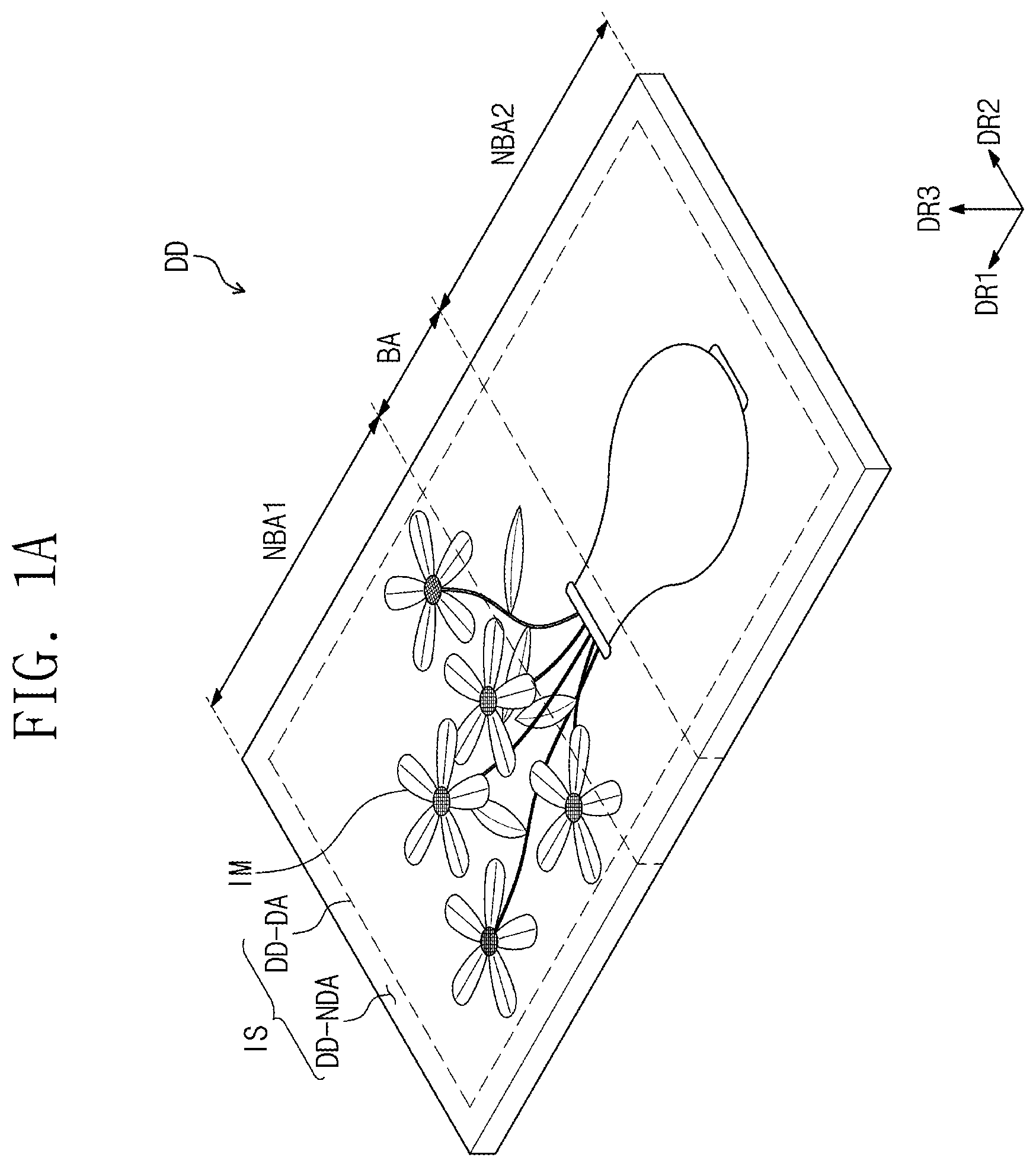
A is a perspective view illustrating a display device DD in a normal mode, according to an exemplary embodiment. B is a perspective view illustrating the display device DD of A in a folded-in mode.
As illustrated in A , in a normal mode, a display surface IS on which an image IM is displayed is parallel to a plane defined by a first directional axis DR 1 and a second directional axis DR 2 . A normal direction of the display surface IS (i.e., a thickness direction of the display device DD) is parallel to a third directional axis DR 3 . A front surface (or a top surface) and a back surface (or a bottom surface) of each of members are defined along the third directional axis DR 3 . However, directions indicated by the first to third directional axes DR 1 , DR 2 , and DR 3 may be relative directions and may be changed into other directions. Hereinafter, first to third directions are the directions respectively indicated by the first to third directional axes DR 1 , DR 2 , and DR 3 and are indicated by the same reference designators as the first to third directional axes DR 1 , DR 2 , and DR 3 . In the present embodiment, a flexible display device is illustrated. However, embodiments of the inventive concepts are not limited thereto. In certain embodiments, the display device DD according to the present embodiment may be a flat display device.
A and 1 B illustrate a foldable display device as an example of the display device DD. However, the display device DD according to the exemplary embodiments may be, but not limited to, a rollable display device. The display device DD according to the exemplary embodiments may be used in large-sized electronic devices (e.g., televisions and monitors) and small and middle-sized electronic devices (e.g., portable phones, tablets, car navigation units, game consoles, and smart watches).
As illustrated in A , the display surface IS of the display device DD may include a plurality of areas. The display device DD includes a display area DD-DA and a non-display area DD-NDA adjacent to the display area DD-DA. The image IM is displayed in the display area DD-DA. An image is not displayed in the non-display area DD-NDA. A flower vase image is illustrated as an example of the image IM in A . For example, the display area DD-DA may have a quadrilateral shape. The non-display area DD-NDA may surround the display area DD-DA. However, embodiments of the inventive concepts are not limited thereto. The shapes of the display area DD-DA and the non-display area DD-NDA may take various other shapes and forms without departing from the scope of the inventive concepts.
Even though not shown in the drawings, the display device DD may include a housing. The housing may be disposed at an outer periphery of the display device DD and may receive internal parts of the display device DD.
As illustrated in A and 1 B , the display device DD may include a plurality of areas defined according to an operation mode. The display device DD may include a bending area BA bent on the basis of a bending axis BX, a first non-bending area NBA 1 , and a second non-bending area NBA 2 . The first and second non-bending areas NBA 1 and NBA 2 are not bent.
As illustrated in B , the display device DD may be bent inwards such that the display surface IS of the first non-bending area NBA 1 faces the display surface IS of the second non-bending area NBA 2 . The bending state in which the display surface IS of the first non-bending area NBA 1 faces the display surface IS of the second non-bending area NBA 2 is defined as a folded-in mode. A state illustrated in A , in which display device DD is not in the folded-in mode, may be defined as a normal mode.
In some embodiments, the display device DD may include a plurality of bending areas BA. As shown in B , the bending area BA may be defined or designed to be parallel to the second directional axis DR 2 . In addition, the bending area BA may be defined or designed to correspond to a manner in which a user operates the display device DD. For example, the bending area BA may be defined or designed to be parallel to the first directional axis DR 1 or may be defined or designed in a diagonal direction, unlike B . An area (or size) of the bending area BA may not be fixed but may be determined according to a radius of curvature. In some embodiments of the inventive concepts, the display device DD may be repeatedly operated only between the operation modes illustrated in A and 1 B .
A is a perspective view illustrating a display device DD in a normal mode, according to some embodiments of the inventive concepts. B is a perspective view illustrating the display device DD of A in a folded-in mode. A and 2 B illustrate an example of a display device DD of which a folding portion is different from that of the display device DD illustrated in A and 1 B . As such, embodiments of the inventive concepts are not limited to any number of bending areas BA and non-bending areas NBA of the display device DD or any position of bending areas BA of the display device DD.
is a cross-sectional view illustrating a display device DD according to an exemplary embodiment of the inventive concepts. illustrates a cross section defined by the second directional axis DR 2 and the third directional axis DR 3 .
As illustrated in , the display device DD includes a protective film PM, a window WM, a display module DM, a first adhesive member AM 1 , and a second adhesive member AM 2 . The display module DM is disposed between the protective film PM and the window WM. The first adhesive member AM 1 couples the display module DM and the protective film PM to each other, and the second adhesive member AM 2 couples the display module DM and the window WM to each other. In some exemplary embodiments, the first adhesive member AM 1 and the second adhesive member AM 2 may be omitted. Each of the protective film PM and the window WM may be continuously formed through a coating process.
The protective film PM protects the display module DM. The protective film PM provides or includes a first outer surface OS-L exposed outward and an adhesive surface adhered to the first adhesive member AM 1 . The protective film PM prevents external moisture from permeating into the display module DM and may absorb energy from an external impact.
The protective film PM may include a plastic film as a base layer. The protective film PM may include a plastic film, the plastic film being one selected from a group including polyethersulphone (PES), polyacrylate (PAR), polyetherimide (PEI), polyethyelene napthalate (PEN), polyethyeleneterepthalate (PET), polyphenylene sulfide (PPS), polyallylate, polyimide (PI), polycarbonate (PC), poly(aryleneether sulfone), and any combination thereof.
The material of the protective film PM is not limited to plastic resins, and may include an organic/inorganic composite material. For example, the protective film PM may include a porous organic layer and an inorganic material filling pores of the porous organic layer. The protective film PM may further include a functional layer formed on the plastic film. The functional layer may include a resin layer. The functional layer may be formed by a coating method.
The window WM may protect the display module DM from an external impact and may provide an input surface to a user. The window WM provides or includes a second outer surface OS-U exposed outward and an adhesive surface adhered to the second adhesive member AM 2 . The display surface IS illustrated in A and 1 B may be the second outer surface OS-U. The second outer surface OS-U may be a touch sensing surface for sensing a touch of a user.
In the display devices DD illustrated in A, 1 B, 2 A, and 2 B , the window WM may not be disposed in the bending area BA. However, embodiments of the inventive concepts are not limited thereto. In certain embodiments, the window WM may also be disposed in the bending area BA.
The display module DM includes a display panel DP and a sensor unit TS which may be integrally formed with each other by continuous processes. The display panel DP may include a light-emitting device. The display panel DP generates an image IM (see A ) corresponding to inputted image data. The display panel DP provides or includes a first display panel surface BS 1 -L and a second display panel surface BS 1 -U, which are opposite to each other in the thickness direction DR 3 . A process of forming the display panel DP may include a low-temperature polycrystalline silicon (LTPS) process or a low-temperature polycrystalline oxide (LTPO) process.
The sensor unit TS obtains information of coordinates of external input. The sensor unit TS may be disposed directly on the second display panel surface BS 1 -U. In the present exemplary embodiment, the sensor unit TS may be integrally formed with the display panel DP by the continuous processes.
Even though not shown in the drawings, the display module DM according to some embodiments of the inventive concepts may further include an anti-reflection layer. The anti-reflection layer may include a color filter, a stack structure of a conductive layer/a dielectric layer/a conductive layer, or an optical member. The anti-reflection layer may absorb, destructively interfere with, or polarize light incident from the outside to reduce reflexibility of external light.
Each of the first and second adhesive members AM 1 and AM 2 may be an optically clear adhesive (OCA) film, an optically clear resin (OCR), or a pressure sensitive adhesive (PSA) film. Each of the first and second adhesive members AM 1 and AM 2 may include, but not limited to, a photo-curing adhesive material or a thermosetting adhesive material.
Even though not shown in the drawings, the display device DD may further include a frame structure that supports the functional layers to maintain the states illustrated in A, 1 B, 2 A, and 2 B . The frame structure may include a joint structure or a hinge structure.
In some embodiments, the sensor unit TS may be single-layered. In other words, the sensor unit TS may include a single conductive layer. Here, the single conductive layer means that a conductive layer may form a pattern separated by an insulating material in the same layer. A stack structure of a first metal layer/a second metal layer/a metal oxide layer corresponds to a single conductive layer, and a stack structure of a metal layer/an insulating layer/a metal oxide layer corresponds to a double conductive layer.
The single conductive layer is patterned to form a plurality of touch sensors and a plurality of touch signal lines. In other words, the touch sensors of the sensor unit TS may be disposed on the same layer. The touch sensors may be disposed directly on a thin film sealing layer TFE. In addition, a portion of each of the touch signal lines may be disposed on the same layer as the touch sensors.
The touch signal lines and the touch sensors may include indium-tin oxide (ITO), indium-zinc oxide (IZO), zinc oxide (ZnO), indium-tin-zinc oxide (ITZO), PEDOT, metal nanowire, and/or graphene. The touch signal lines and the touch sensors may include a metal layer, e.g., molybdenum, silver, titanium, copper, aluminum, or any alloy thereof. The touch signal lines and the touch sensors may include the same material or materials different from each other.
However, embodiments of the inventive concepts are not limited thereto. In certain embodiments, the sensor unit TS may have a multi-layered structure including a plurality of conductive layers.
is a plan view illustrating a display panel DP according to an exemplary embodiment of the inventive concepts. is an equivalent circuit diagram of a pixel PX according to an exemplary embodiment of the inventive concepts. are partial cross-sectional views illustrating a display panel DP according to an exemplary embodiment of the inventive concepts.
As illustrated in , the display panel DP includes a display area DA and a non-display area NDA when viewed in a plan view. The display area DA and the non-display area NDA of the display panel DP correspond to the display area DD-DA and the non-display area DD-NDA of the display device DD in A, 2 A, 2 B , respectively. However, the display area DA and the non-display area NDA of the display panel DP may not need to be the same as the display area DD-DA and the non-display area DD-NDA of the display device DD but may be changed according to a structure and/or a design of the display panel DP.
The display panel DP includes a plurality of signal lines SGL and a plurality of pixels PX. The display area DA is defined as an area in which the plurality of pixels PX is disposed. In the present embodiment, the non-display area NDA may be defined along a border of the display area DA.
The plurality of signal lines SGL may include gate lines GL, data lines DL, a power line PL, and a control signal line CSL. Each of the gate lines GL is connected to corresponding ones of the plurality of pixels PX, and each of the data lines DL is connected to corresponding ones of the plurality of pixels PX. The power line PL is connected to the plurality of pixels PX. A gate driving circuit DCV to which the gate lines GL are connected may be disposed in one side portion of the non-display area NDA. The control signal line CSL may provide control signals to the gate driving circuit DCV.
One or some of the gate lines GL, the data lines DL, the power line PL and the control signal line CSL may be disposed on one layer, and another or others of the gate lines GL, the data lines DL, the power line PL and the control signal line CSL may be disposed on another layer different from the one layer. The gate lines GL, the data lines DL, the power line PL and the control signal line CSL disposed on the one layer may be defined as first signal lines, and the signal lines disposed on the another layer may be defined as second signal lines. The signal lines disposed on still another layer may be defined as third signal lines.
Each of the gate lines GL, the data lines DL, the power line PL and the control signal line CSL may include a signal interconnection portion and a display panel pad PD-DP connected to an end of the signal interconnection portion. The signal interconnection portion may be defined as a portion of each of the gate lines GL, the data lines DL, the power line PL and the control signal line CSL except the display panel pads PD-DP.
The display panel pads PD-DP may be formed in the same process as transistors for driving the pixels PX. For example, the display panel pads PD-DP may be formed in the same low-temperature polycrystalline silicon (LTPS) process or low-temperature polycrystalline oxide (LTPO) process as the transistors for driving the pixels PX.
In some embodiments, the display panel pads PD-DP may include a control pad CSL-P, a data pad DL-P, and a power pad PL-P. A gate pad is not illustrated. However, the gate pad may overlap with the gate driving circuit DCV and may be connected to the gate driving circuit DCV. Even though not indicated in the drawings, a portion of the non-display area NDA, in which the control pad CSL-P, the data pad DL-P and the power pad PL-P are arranged, may be defined as a pad area. As described later, pads of the sensor unit TS may be disposed to be adjacent to the display panel pads PD-DP described above.
The pixel PX connected to one gate line GL, one data line DL and the power line PL is illustrated as an example in . However, the configuration of the pixel PX is not limited to but may be variously modified.
The pixel PX includes a light-emitting device OLED used as a display element. The light-emitting device OLED may be a front surface light-emitting type diode or a back surface light-emitting type diode. Alternatively, the light-emitting device OLED may be a both surface light-emitting type diode. The pixel PX includes a first transistor TFT 1 (or a switching transistor), a second transistor TFT 2 (or a driving transistor) and a capacitor CAP which constitute a circuit part for driving the light-emitting device OLED. The light-emitting device OLED generates light by an electrical signal provided from the transistors TFT 1 and TFT 2 .
The first transistor TFT 1 outputs a data signal applied to the data line DL in response to a scan signal applied to the gate line GL. The capacitor CAP is charged with a voltage corresponding to the data signal received from the first transistor TFT 1 .
The second transistor TFT 2 is connected to the light-emitting device OLED. The second transistor TFT 2 controls a driving current flowing through the light-emitting device OLED in response to the amount of charges stored in the capacitor CAP. The light-emitting device OLED emits light while the second transistor TFT 2 is turned-on.
is a cross-sectional view of a portion corresponding to the first transistor TFT 1 and the capacitor CAP of the equivalent circuit illustrated in . is a cross-sectional view of a portion corresponding to the second transistor TFT 2 and the light-emitting device OLED of the equivalent circuit illustrated in .
As illustrated in , a first circuit layer CL 1 is disposed on a base layer SUB. A semiconductor pattern AL 1 (hereinafter, referred to as ‘a first semiconductor pattern’) of the first transistor TFT 1 and a semiconductor pattern AL 2 (hereinafter, referred to as ‘a second semiconductor pattern’) of the second transistor TFT 2 are disposed on the base layer SUB, or may be disposed on top of organic/inorganic layers BR, BF. Each of the first and second semiconductor patterns AL 1 and AL 2 may include at least one of amorphous silicon, poly-silicon, or a metal oxide semiconductor. Here, the first and second semiconductor patterns AL 1 and AL 2 may include the same material or different materials from each other.
The first circuit layer CL 1 may include organic/inorganic layers BR, BF, 12 , 14 , and 16 , the first transistor TFT 1 , the second transistor TFT 2 , and electrodes E 1 and E 2 . The organic/inorganic layers BR, BF, 12 , 14 , and 16 may be a functional layer BR and BF, a first insulating layer 12 , a second insulating layer 14 , and a third insulating layer 16 .
The functional layer BR and BF may be disposed on one surface of the base layer SUB. The functional layer BR and BF includes at least one of a barrier layer BR or a buffer layer BF. The first semiconductor pattern AL 1 and the second semiconductor pattern AL 2 may be disposed on the barrier layer BR or the buffer layer BF.
The first insulating layer 12 is disposed on the base layer SUB and covers the first semiconductor pattern AL 1 and the second semiconductor pattern AL 2 . The first insulating layer 12 includes an organic layer and/or an inorganic layer. In particular, the first insulating layer 12 may include a plurality of inorganic thin layers. The plurality of inorganic thin layers may include a silicon nitride layer and a silicon oxide layer.
A control electrode GE 1 (hereinafter, referred to as ‘a first control electrode’) of the first transistor TFT 1 and a control electrode GE 2 (hereinafter, referred to as ‘a second control electrode’) of the second transistor TFT 2 are disposed on the first insulating layer 12 . A first electrode E 1 of the capacitor CAP is disposed on the first insulating layer 12 . The first control electrode GE 1 , the second control electrode GE 2 , the first electrode E 1 , and the gate lines GL (see ) may be formed using the same photolithography process. In other words, the first electrode E 1 and the gate lines GL may have the same material and the same stack structure and may be disposed on the same layer.
The second insulating layer 14 is disposed on the first insulating layer 12 and covers the first control electrode GE 1 , the second control electrode GE 2 , and the first electrode E 1 . The second insulating layer 14 includes an organic layer and/or an inorganic layer. In particular, the second insulating layer 14 may include a plurality of inorganic thin layers. The plurality of inorganic thin layers may include a silicon nitride layer and a silicon oxide layer.
The data lines DL (see ) may be disposed on the second insulating layer 14 . An input electrode SE 1 (hereinafter, referred to as ‘a first input electrode’) and an output electrode DE 1 (hereinafter, referred to as ‘a first output electrode’) of the first transistor TFT 1 are disposed on the second insulating layer 14 . An input electrode SE 2 (hereinafter, referred to as ‘a second input electrode’) and an output electrode DE 2 (hereinafter, referred to as ‘a second output electrode’) of the second transistor TFT 2 are disposed on the second insulating layer 14 . The first input electrode SE 1 is branched from one of the corresponding data lines DL. The power line PL (see ) and the data lines DL may be disposed on the same layer. The second input electrode SE 2 may be branched from the power line PL.
A second electrode E 2 of the capacitor CAP is disposed on the second insulating layer 14 . The second electrode E 2 , the data lines DL and the power line PL may be formed using the same photolithography process, may have the same material and the same stack structure, and may be disposed on the same layer.
The first input electrode SE 1 and the first output electrode DE 1 are connected to portions of the first semiconductor pattern AL 1 through a first through-hole CH 1 and a second through-hole CH 2 penetrating the first and second insulating layers 12 and 14 , respectively. The first output electrode DE 1 may be electrically connected to the first electrode E 1 . For example, the first output electrode DE 1 may be connected to the first electrode E 1 through a through-hole (not shown) penetrating the second insulating layer 14 . The second input electrode SE 2 and the second output electrode DE 2 are connected to portions of the second semiconductor pattern AL 2 through a third through-hole CH 3 and a fourth through-hole CH 4 penetrating the first and second insulating layers 12 and 14 , respectively. Meanwhile, in other embodiments, the first transistor TFT 1 and the second transistor TFT 2 may have bottom gate structures.
The third insulating layer 16 is disposed on the second insulating layer 14 and covers the first input electrode SE 1 , the first output electrode DE 1 , the second input electrode SE 2 , and the second output electrode DE 2 . The third insulating layer 16 includes an organic layer and/or an inorganic layer. In particular, the third insulating layer 16 may include an organic material to provide a flat surface.
One of the first, second, and third insulating layers 12 , 14 , and 16 may be omitted according to a circuit structure of the pixel PX. Each of the second and third insulating layers 14 and 16 may be defined as an interlayer insulating layer. The interlayer insulating layer is disposed between a conductive pattern disposed thereunder and a conductive pattern disposed thereon to insulate the conductive patterns from each other.
A light-emitting device layer ELL is disposed on the third insulating layer 16 . The light-emitting device layer ELL includes a pixel-defining layer PXL and the light-emitting device OLED. An anode AE is disposed on the third insulating layer 16 . The anode AE is connected to the second output electrode DE 2 through a fifth through-hole CH 5 penetrating the third insulating layer 16 . An opening OP is defined in the pixel-defining layer PXL. The opening OP of the pixel-defining layer PXL exposes at least a portion of the anode AE.
The light-emitting device layer ELL includes a light emitting area PXA and a non-light emitting area NPXA adjacent to the light emitting area PXA. The non-light emitting area NPXA may surround the light emitting area PXA. In the present embodiment, the light emitting area PXA is defined to correspond to the anode AE. However, the light emitting area PXA is not limited thereto. In other words, the light emitting area PXA is defined as an area from which light is generated. In certain embodiments, the light emitting area PXA may be defined to correspond to the portion of the anode AE, which is exposed by the opening OP.
A hole control layer HCL may be disposed in both the light emitting area PXA and the non-light emitting area NPXA. Even though not shown in the drawings, a common layer such as the hole control layer HCL may be formed in common for the plurality of pixels PX (see ).
A light-emitting layer EML is disposed on the hole control layer HCL. The light-emitting layer EML may be disposed in only an area corresponding to the opening OP. In other words, the light-emitting layers EML of the pixels PX may be separated from each other.
The light-emitting layer EML may include an organic material or an inorganic material.
An electron control layer ECL is disposed on the light-emitting layer EML. A cathode CE is disposed on the electron control layer ECL. The cathode CE is disposed in common with the plurality of pixels PX.
In the present embodiment, a patterned light-emitting layer EML is illustrated as an example. In certain embodiments, the light-emitting layer EML may be disposed in common with the plurality of pixels PX. At this time, the light-emitting layer EML may generate white light. In some embodiments, the light-emitting layer EML may have a multi-layered structure.
In the present embodiment, a thin film sealing layer TFE directly covers the cathode CE. In some embodiments, a capping layer covering the cathode CE may further be disposed. In this case, the thin film sealing layer TFE may directly cover the capping layer. The thin film sealing layer TFE may include an organic layer including an organic material and an inorganic layer including an inorganic material.
is a plan view illustrating a sensor unit TS of a display module according to some embodiments of the inventive concepts. The sensor unit TS of the display module includes a touch sensing area TA and a non-touch sensing area NTA when viewed in a plan view.
The touch sensors for sensing a touch may be disposed in the touch sensing area TA. Touch signal lines for electrically connecting the touch sensors to sensor unit pads PD-TS may be disposed in the non-touch sensing area NTA.
The sensor unit pads PD-TS are electrically connected to pads PD-PCB of a printed circuit board PCB. An integrated circuit DIC may be disposed on the printed circuit board PCB. The integrated circuit DIC may be formed by a chip-on-flexible printed circuit (COF) method. The integrated circuit DIC may control the sensor unit TS.
In some embodiments, the integrated circuit DIC may control the display panel DP as well as the sensor unit TS.
is an enlarged view of a portion ‘AA’ of . A and 10 B are cross-sectional views taken along a line II-II′ of .
Referring to A , the display area DA includes a plurality of the light emitting areas PXA and the non-light emitting area NPXA surrounding the light emitting areas PXA. A touch sensor SP may have a mesh shape overlapping with the non-light emitting area NPXA.
The touch sensor SP includes a plurality of vertical portions SP-C extending in a first direction DR 1 and a plurality of horizontal portions SP-L extending in a second direction DR 2 . The plurality of vertical portions SP-C and the plurality of horizontal portions SP-L may be defined as a mesh line. A width of the mesh line may be several micrometers.
The plurality of vertical portions SP-C and the plurality of horizontal portions SP-L are connected to each other to form a plurality of touch openings TS-OP. In the present embodiment, the touch openings TS-OP correspond to the light emitting areas PXA, respectively. However, exemplary embodiments of the inventive concepts are not limited thereto. In certain embodiments, one touch opening TS-OP may correspond to two or more light emitting areas PXA. A illustrate the touch sensor SP exposed outward. Alternatively, the display module DM may further include an insulating layer that is disposed on the thin film sealing layer TFE to cover the touch sensor SP.
Referring to B , a touch sensor SP-MR may include a first touch electrode MLT 1 , an insulating pattern CNT, and a second touch electrode MLT 2 . The insulating pattern CNT insulates the first touch electrode MLT 1 from the second touch electrode MLT 2 .
Each of the first and second touch electrodes MLT 1 and MLT 2 may reflect incident light. Thus, the first and second touch electrodes MLT 1 and MLT 2 may provide a mirror function to a user.
A is a plan view illustrating touch sensors SP disposed in a touch sensing area TA. B is a cross-sectional view taken along a line I-I′ of B to illustrate a display device according to some embodiments of the inventive concepts.
Referring to A , a sensor unit TS includes touch sensors SP and connection patterns CP, which are disposed in the touch sensing area TA.
The touch sensors SP may include first touch sensors SP 1 and second touch sensors SP 2 . The first touch sensors SP 1 extend in the first direction DR 1 and are arranged in the second direction DR 2 . Each of the first touch sensors SP 1 may have a mesh shape in which a plurality of touch openings TS-OP is defined.
The second touch sensors SP 2 may be insulated from the first touch sensors SP 1 by insulating patterns CNT (see B ). The insulating patterns CNT may include an inorganic material or an organic material. The inorganic material may include silicon oxide or silicon nitride. The organic material may include at least one of an acrylic-based resin, a methacrylic-based resin, polyisoprene, a vinyl-based resin, an epoxy-based resin, a urethane-based resin, a cellulose-based resin, or a perylene-based resin.
Each of the second touch sensors SP 2 may have a mesh shape in which a plurality of touch openings TS-OP is defined.
The connection patterns CP may include first connection patterns CP 1 and second connection patterns CP 2 . Each of the first connection patterns CP 1 connects adjacent two of the first touch sensors SP 1 . Each of the second connection patterns CP 2 connects adjacent two of the second touch sensors SP 2 .
In some embodiments, the first connection patterns CP 1 or the second connection patterns CP 2 may have a bridge function.
The first touch sensors SP 1 may be capacitively coupled to the second touch sensors SP 2 .
In some exemplary embodiments, the first touch sensors SP 1 may transmit electric fields, and the second touch sensors SP 2 may receive the electric fields transmitted from the first touch sensors SP 1 .
In other exemplary embodiments, the second touch sensors SP 2 may transmit electric fields, and the first touch sensors SP 1 may receive the electric fields transmitted from the second touch sensors SP 2 .
The above mentioned shapes of the first and second touch sensors SP 1 and SP 2 are illustrated as examples. However, embodiments of the inventive concepts are not limited thereto. In certain exemplary embodiments, each of the first and second touch sensors SP 1 and SP 2 may have a bar shape having a uniform width.
The first touch sensors SP 1 and the second touch sensors SP 2 may be disposed symmetrically with respect to the bending axis BX.
Referring to B , the first touch sensor SP 1 overlaps with the second touch sensor SP 2 in the folded-in mode in which the display device DD is folded along the bending axis BX. At this time, the first touch sensor SP 1 and the second touch sensor SP 2 overlapping with each other are capacitively coupled to each other. When external pressure is applied, a capacitance between the first and second touch sensors SP 1 and SP 2 capacitively coupled to each other may be varied and the display device DD may sense the variation in the capacitance to measure the external pressure.
As described above, the display device DD may sense the touch of the user in the normal mode and may sense the pressure applied by the user in the folded-in mode. However, embodiments of the inventive concepts are not limited thereto. In certain embodiments, the sensor unit TS may not sense the applied pressure.
A is a plan view illustrating touch sensors SP disposed in a touch sensing area TA. B is a cross-sectional view taken along the line I-I′ of B to illustrate a display device according to an exemplary embodiment.
Referring to A , a sensor unit TS- 1 includes touch sensors SP- 1 and connection patterns CP, which are disposed in the touch sensing area TA.
The touch sensors SP- 1 may include first touch sensors SP 1 - 1 and second touch sensors SP 2 - 1 .
Unlike the touch sensors SP illustrated in A and 11 B , the same kind of the touch sensors SP- 1 are symmetrical with respect to the bending axis BX in A . For example, one of the first touch sensors SP 1 - 1 and another of the first touch sensors SP 1 - 1 are disposed symmetrically with respect to the bending axis BX. In addition, one of the second touch sensors SP 2 - 1 and another of the second touch sensors SP 2 - 1 are disposed symmetrically with respect to the bending axis BX.
Referring to B , the one of the first touch sensors SP 1 - 1 overlaps with the another of the first touch sensor SP 1 - 1 in the folded-in mode in which the display device DD- 1 is folded on the bending axis BX. At this time, the first touch sensors SP 1 - 1 overlapping with each other are capacitively coupled to each other. When external pressure is applied, a capacitance between the first touch sensors SP 1 - 1 capacitively coupled to each other may be varied and the display device DD may sense the variation in the capacitance to measure the external pressure.
In the normal mode, the first touch sensors SP 1 - 1 of a display device DD- 1 selectively performs one of a function transmitting electric fields and a function receiving the electric fields. However, in the folded-in mode of the display device DD- 1 , one of the overlapping two first touch sensors SP 1 - 1 transmits the electric field and the other of the overlapping two first touch sensors SP 1 - 1 receives the electric field.
In the normal mode, the second touch sensors SP 2 - 1 of the display device DD- 1 selectively performs one of the function transmitting electric fields and the function receiving the electric fields. However, in the folded-in mode of the display device DD- 1 , one of overlapping two second touch sensors SP 2 - 1 transmits the electric field and the other of the overlapping two second touch sensors SP 2 - 1 receives the electric field.
The integrated circuit DIC (see ) may control the role change of the first and second touch sensors SP 1 - 1 and SP 2 - 1 according to the mode change between the normal mode and the folded-in mode.
A is a perspective view illustrating a display device DD 1 in a normal mode, according to exemplary embodiments. B is a perspective view illustrating the display device DD 1 of A in a folded-outward mode.
The display device DD 1 in the normal mode in A may be substantially the same as the display device DD in the normal mode in A , and thus the descriptions thereto will be omitted.
As illustrated in B , the display device DD 1 may be outer-bent such that a display surface IS of the display device DD 1 is exposed outward. In the present specification, a state in which a back surface of a first non-bending area NBA 1 faces a back surface of a second non-bending area NBA 2 is defined as the folded-outward mode. A state illustrated in A , in which display device DD 1 is not in the folded-outward mode, may be defined as the normal mode.
A is a perspective view illustrating a display device DD 1 in a normal mode, according to exemplary embodiments. B is a perspective view illustrating the display device DD 1 of A in a folded-outward mode. A and 14 B illustrate an example of a display device DD of which a folding portion is different from that of the display device DD 1 illustrated in A and 13 B . As such, embodiments of the inventive concepts are not limited to the numbers of the bending area BA and the non-bending area NBA of the display device DD 1 and a position of the bending area of the display device DD 1 .
A is a cross-sectional view taken along a line of A to illustrate a display device according to an exemplary embodiment. B is a cross-sectional view taken along a line IV-IV′ of B to illustrate a display device according to an exemplary embodiment.
Referring to A , a force sensor FSS is disposed under the display module DM. The force sensor FSS includes a first force-sensing electrode FS 1 and a second force-sensing electrode FS 2 . The first force-sensing electrode FS 1 and the second force-sensing electrode FS 2 may be symmetrical with respect to the bending axis BX.
Referring to B , the first force-sensing electrode FS 1 overlaps with the second force-sensing electrode FS 2 in the folded-outward mode. The first and second force-sensing electrodes FS 1 and FS 2 overlapping with each other are capacitively coupled to each other. When external pressure is applied, a capacitance between the capacitively coupled first and second force-sensing electrodes FS 1 and FS 2 may be varied and the display device DD 1 may sense the variation in the capacitance to measure the external pressure.
A is a cross-sectional view taken along the line III-III′ of A to illustrate a display device according to an exemplary embodiment. B is a cross-sectional view taken along the line IV-IV′ of B to illustrate a display device according to an exemplary embodiment. C illustrates strain gauges SG 1 and SG 2 of A .
Referring to A , a force sensor FSS- 1 is disposed under the display module DM. The force sensor FSS- 1 includes strain gauges SG 1 and SG 2 . The strain gauges SG 1 and SG 2 may include a first strain gauge SG 1 and a second strain gauge SG 2 . The first strain gauge SG 1 may be disposed to overlap with the first non-bending area NBA 1 , and the second strain gauge SG 2 may be disposed to overlap with the second non-bending area NBA 2 .
The strain gauge is used to measure pressure, torque or stress by using a pressure resistance effect, which means that a resistance value of a resistor formed of a metal or semiconductor is varied when the resistor is deformed.
Referring to C , a metal pattern of each of the strain gauges SG 1 and SG 2 may have specific directivity. A direction of the metal pattern of one of the strain gauges SG 1 and SG 2 may be perpendicular to a direction of the metal pattern of another strain gauge that is adjacent to the one strain gauge. In this manner, the strain gauges SG 1 and SG 2 may be disposed such that the directions of the metal patterns are perpendicular to each other, and thus the sensitivity of the measured pressure may be improved.
is a perspective view illustrating a display device DD 2 according to exemplary embodiments. The display device DD 2 is a both surface light-emitting display device that provides images IM 1 and IM 2 through its front surface and back surface. The display device DD 2 provides a first image IM 1 through its front surface. In , a flower vase image is illustrated as an example of the first image IM 1 . The display device DD 2 provides a second image IM 2 through its back surface. In , a bear doll image is illustrated as an example of the second image IM 2 .
is a partial cross-sectional view illustrating a display device DD 2 according to exemplary embodiments. The display device DD 2 includes a display panel DP- 1 , a sensor unit TS, a first force sensor FSS 1 , and a second force sensor FSS 2 . The display panel DP- 1 includes a transparent base layer SUB-TP, an insulating layer 16 - 1 , and a light-emitting device layer ELL- 1 .
The transparent base layer SUB-TP may transmit at least a portion of incident light. For example, the transparent base layer SUB-TP may include glass.
The insulating layer 16 - 1 is disposed on the transparent base layer SUB-TP. A function and a material of the insulating layer 16 - 1 may be substantially the same as those of the third insulating layer 16 of , and thus the descriptions thereto will be omitted.
The light-emitting device layer ELL- 1 is disposed on the insulating layer 16 - 1 . The light-emitting device layer ELL- 1 includes a light-emitting device OLED- 1 . The light-emitting device OLED- 1 may include a front surface light emitting area LA-F and a back surface light emitting area LA-B.
The light-emitting device OLED- 1 includes a first reflection layer RF 1 , a first anode AE 1 , a second anode AE 2 , a light-emitting layer EML, a cathode CE, and a second reflection layer RF 2 .
The first reflection layer RF 1 is disposed on the insulating layer 16 - 1 and overlaps with the front surface light emitting area LA-F. The first reflection layer RF 1 may reflect incident light.
The first anode AE 1 is disposed on the first reflection layer RF 1 and overlaps with the front surface light emitting area LA-F. The second anode AE 2 is disposed on the insulating layer 16 - 1 and overlaps with the back surface light emitting area LA-B.
The light-emitting layer EML is disposed on the first anode AE 1 and the second anode AE 2 and overlaps with the front surface light emitting area LA-F and the back surface light emitting area LA-B.
The cathode CE is disposed on the light-emitting layer EML and overlaps with the front surface light emitting area LA-F and the back surface light emitting area LA-B.
The second reflection layer RF 2 is disposed on the cathode CE and overlaps with the back surface light emitting area LA-B. The second reflection layer RF 2 may reflect incident light.
Light generated in the light-emitting layer EML is reflected by the first reflection layer RF 1 so as to be emitted to the front surface. Light generated in the light-emitting layer EML is reflected by the second reflection layer RF 2 so as to be emitted to the back surface. Thus, the light-emitting device OLED- 1 may emit the light to the front surface and the back surface.
The first force sensor FSS 1 is disposed on the second reflection layer RF 2 and overlaps with the back surface light emitting area LA-B. The first force sensor FSS 1 may sense pressure applied to the display device DD 2 . The first force sensor FSS 1 may include a strain gauge.
The sensor unit TS may be disposed on the first force sensor FSS 1 .
The second force sensor FSS 2 is disposed under the display panel DP- 1 . When the display device DD 2 is folded, the second force sensor FSS 2 may sense pressure applied to the display device DD 2 .
The second force sensor FSS 2 includes a first force-sensing electrode FS 1 and a second force-sensing electrode FS 2 . The first and second force-sensing electrodes FS 1 and FS 2 may be substantially the same as described with reference to A , and thus the descriptions thereto will be omitted.
is a partial cross-sectional view illustrating a display device DD 2 - 1 according to an exemplary embodiment.
The display device DD 2 - 1 includes a display panel DP- 2 , a sensor unit TS, a first force sensor FSS 1 , and a second force sensor FSS 2 . The display panel DP- 2 includes the transparent base layer SUB-TP, the insulating layer 16 - 1 , the light-emitting device layer ELL- 1 , and a planarization layer FLL 1 .
The planarization layer FLL 1 covers the light-emitting device layer ELL- 1 and provides a flat or planarized surface. The planarization layer FLL 1 may include an organic material. In some embodiments, the planarization layer FLL 1 may act as a sealing material sealing the light-emitting device layer ELL- 1 .
The first force sensor FSS 1 may be disposed on the planarization layer FLL 1 . The first force sensor FSS 1 may be covered with an additional planarization layer FLL 2 .
Other elements or components of the display device DD 2 - 1 may be substantially the same as described with reference to , and thus the descriptions thereto will be omitted.
is a partial cross-sectional view illustrating a display device DD 2 - 2 according to exemplary embodiments.
The display device DD 2 - 2 includes the display panel DP- 1 , a reflection member MR, the first force sensor FSS 1 , and the second force sensor FSS 2 .
The reflection member MR is disposed on the first force sensor FSS 1 and overlaps in plan view with the front surface light emitting area LA-F and the back surface light emitting area LA-B. The reflection member MR may reflect light to provide a mirror function to a user.
The reflection member MR may be capacitively coupled to the first force sensor FSS 1 to sense a touch of a user. For example, the reflection member MR and the first force sensor FSS 1 may sense a touch by a self-cap method.
is a cross-sectional view illustrating a display device DD 2 - 3 according to exemplary embodiments. The display device DD 2 - 3 includes a first display module DM 1 , a second display module DM 2 , and a force sensor FSS 3 . The first and second display modules DM 1 and DM 2 may be substantially the same as described with reference to to 7 , and thus the descriptions thereto will be omitted.
The force sensor FSS 3 is disposed between the first display module DM 1 and the second display module DM 2 . The force sensor FSS 3 may sense pressure applied to the display device DD 2 - 3 .
, 23 , 24 , 25 , and 26 are cross-sectional views illustrating force sensors FSS 3 , FSS 3 - 1 , FSS 3 - 2 , FSS 3 - 3 , and FSS 3 - 4 according to exemplary embodiments.
Referring to , the force sensor FSS 3 includes an insulating layer LPI, a buffer layer BF-FSS, a pressure cushion PC, a first force-sensing electrode FS 1 , and a second force-sensing electrode FS 2 . In some embodiments, the force sensor FSS 3 may include the insulating layer LPI, the second force-sensing electrode FS 2 , the buffer layer BF-FSS, the insulating layer LPI, the pressure cushion PC, the insulating layer LPI, the buffer layer BF-FSS, the first force-sensing electrode FS 1 and the insulating layer LPI which may be stacked in the order listed. However, exemplary embodiments are not limited to the stack order of the force sensor FSS 3 . In certain embodiments, the insulating layer LPI, the buffer layer BF-FSS, the pressure cushion PC, the first force-sensing electrode FS 1 and the second force-sensing electrode FS 2 may be stacked in another stack order.
The first force-sensing electrode FS 1 is capacitively coupled to the second force-sensing electrode FS 2 . In some embodiments, the first force-sensing electrode FS 1 may transmit an electric field and the second force-sensing electrode FS 2 may receive the electric field.
In other exemplary embodiments, a function of each of the first and second force-sensing electrodes FS 1 and FS 2 of the force sensor FSS 3 - 3 may be changed according to a driving mode. For example, in a first driving mode, the first force-sensing electrode FS 1 may transmit the electric field and the second force-sensing electrode FS 2 may receive the electric field. In a second driving mode, the second force-sensing electrode FS 2 may transmit the electric field and the first force-sensing electrode FS 1 may receive the electric field.
Referring to , the first force-sensing electrode FS 1 of the force sensor FSS 3 - 1 may be electrically connected to the sensor unit TS of the first display module DM 1 through a sixth through-hole CH 6 . The second force-sensing electrode FS 2 of the force sensor FSS 3 - 1 may be electrically connected to the sensor unit TS of the second display module DM 2 through a seventh through-hole CH 7 . In this example, the force sensor FSS 3 - 1 may be supplied with an electrical signal from the sensor unit TS and may thus be driven and controlled.
Referring to , first and second force-sensing electrodes FS 1 and FS 2 of the force sensor FSS 3 - 2 may be alternately arranged on the same layer in a lateral direction.
Referring to , the force sensor FSS 3 - 3 may include the insulating layer LPI, the buffer layer BF-FSS, the insulating layer LPI, the second force-sensing electrode FS 2 , the pressure cushion PC, the first force-sensing electrode FS 1 , the insulating layer LPI, the buffer layer BF-FSS and the insulating layer LPI which may be stacked in the order listed.
Referring to , the force sensor FSS 3 - 4 may further include a noise-shielding layer NSL. The noise-shielding layer NSL may be disposed between the insulating layer LPI and the buffer layer BF-FSS. However, exemplary embodiments are not limited to the position of the noise-shielding layer NSL.
The noise-shielding layer NSL may shield noise occurring at the transistors of the display panels DP 1 and DP 2 , and thus the force sensor FSS 3 - 4 may effectively sense the pressure.
, 28 , and 29 illustrate sensor units TS 2 , TS 3 , and TS 4 according to an exemplary embodiment.
Referring to , a touch sensor SP-TS 2 of the sensor unit TS 2 according to an exemplary embodiment may have a stripe pattern shape, unlike the touch sensor of the sensor unit TS described above.
Referring to , each of touch sensors SP-TS 3 and SP-TS 4 of the sensor units TS 3 and TS 4 may have a shape including a plurality of quadrilateral patterns, unlike the touch sensor of the sensor unit TS described above.
In the folded-in mode, the display device according to exemplary embodiments may sense applied pressure through the capacitive type sensor unit for sensing a touch of a user.
The display device according to exemplary embodiments may sense applied pressure through the force sensor in the folded-outward mode.
The display device according to exemplary embodiments may be a both surface display device providing images in both directions and may sense applied pressure through the force sensor.
Although certain exemplary embodiments and implementations have been described herein, other embodiments and modifications will be apparent from this description. Accordingly, the inventive concept is not limited to such embodiments, but rather to the broader scope of the presented claims and various obvious modifications and equivalent arrangements.
Figures (20)
Citations
This patent cites (39)
- US5703436
- US7679093
- US7936121
- US8681140
- US8723813
- US8979291
- US9024907
- US9229589
- US9304348
- US9419065
- US9652098
- US9733757
- US10133373
- US10268294
- US10564742
- US20050041009
- US20060197753
- US20120139834
- US20130193843
- US20140131668
- US20140176421
- US20140339509
- US20150153862
- US20150352437
- US20150378465
- US20160048262
- US20160062498
- US20160109998
- US20160324023
- US20170285837
- US20180004322
- US105676965
- US10-0685844
- US20140065867
- US10-2014-0095279
- US10-2016-0000100
- US10-2016-0039765
- US20160046139
- US10-2017-0047542