Abstract
A transport system is provided. The transport system includes a stocker configured to store an assigned wafer carrier and having a gate port. The transport system also includes a semiconductor apparatus configured to transmit a request signal including a processed time according to a processing wafer carrier loaded on the semiconductor apparatus. The transport system further includes a vehicle configured to transport the assigned wafer carrier from the gate port to the semiconductor apparatus and a control system configured to control the vehicle. When the control system receives the request signal, the control system controls the stocker to transport the assigned wafer carrier inside of the stocker to the gate port at a start time, which is earlier than the processed time, and the control system controls the vehicle to transport the assigned wafer carrier from the gate port to the semiconductor apparatus.
Claims (20)
1. A transport system, comprising: a semiconductor apparatus, configured to process a wafer and transmit a request signal with a request time to a control system, wherein the request signal comprises a processed time of a processing wafer carrier being loaded on a load port of the semiconductor apparatus at the request time, wherein the processed time is defined as an estimated point of time of the request time plus a process period, wherein the processed period is defined as an estimated period during which a plurality of wafers of the processing wafer carrier are processed by the semiconductor apparatus; a vehicle configured to transport an assigned wafer carrier to the semiconductor apparatus along a transport path; and the control system is configured to control the vehicle; wherein at a time of receiving the request signal by the control system, the control system estimates a delivery time according to the processed time plus a detaching period of the processing wafer carrier being detached from the load port, estimates a transport period during which the assigned wafer carrier is transported along the transport path to the load port, and estimates a start time for transporting the assigned wafer carrier to the load port according to the delivery time minus the transport period; wherein the delivery time is an estimated time when the assigned wafer carrier is loaded at the load port at a time later than the processed time and when the processing wafer carrier has been detached from the load port during the detaching period; wherein the control system controls the vehicle to start the transporting of the assigned wafer carrier to the load port at the start time, which is earlier than the processed time.
6. A transport method, comprising: loading a processing wafer carrier at a load port of a semiconductor apparatus at a request time, wherein the processing wafer carrier contains a plurality of wafers; estimating a processed time according to the processing wafer carrier by the semiconductor apparatus, wherein the processed time is an estimated point of time of the request time plus a process period, wherein the processed period is defined as an estimated period during which the plurality of wafers of the processing wafer carrier are processed by the semiconductor apparatus; transmitting a request signal comprising the processed time to a control system by the semiconductor apparatus at the request time; assigning an assigned wafer carrier according to the request signal, and estimating a delivery time according to the processed time plus a detaching period of the processing wafer carrier being detached from the load port by the control system, wherein the delivery time is an estimated time when the assigned wafer carrier is loaded at the load port at a time later than the processed time and when the processing wafer carrier has been detached from the load port during the detaching period; estimating a transport period during which the assigned wafer carrier is transported along a transport path to the load port, and estimating a start time for transporting the assigned wafer carrier to the load port according to the delivery time minus the transport period by the control system; and starting to transport the assigned wafer carrier to the semiconductor apparatus at the start time, which is earlier than the processed time.
17. A transport method, comprising: loading a processing wafer carrier at a load port of a semiconductor apparatus, wherein the processing wafer carrier contains a plurality of wafers; estimating a processed time of the processing wafer carrier by the semiconductor apparatus, wherein the processed time is an estimated point of time that the plurality of wafers of the processing wafer carrier are processed by the semiconductor apparatus; transmitting a request signal comprising the processed time to a control system by the semiconductor apparatus at a request time; assigning an assigned wafer carrier according to the request signal, and estimating a delivery time according to the processed time plus a detaching period of the processing wafer carrier being detached from the load port by the control system, wherein the delivery time is an estimated time when the assigned wafer carrier is loaded at the load port at a time later than the processed time and when the processing wafer carrier has been detached from the load port during the detaching period; estimating a transport period during which the assigned wafer carrier is transported along a transport path to the load port, and estimating a start time for transporting the assigned wafer carrier to the load port according to the delivery time minus the transport period by the control system; and starting to transport the assigned wafer carrier to the load port of the semiconductor apparatus at the start time, which is earlier than the processed time and later than the request time.
Show 17 dependent claims
2. The transport system as claimed in claim 1 , wherein the control system is further configured to stop the vehicle with the assigned wafer carrier at a check position of the transport path to wait for the processing wafer carrier to be transported away from the semiconductor apparatus when the semiconductor apparatus is occupied with the processing wafer carrier.
3. The transport system as claimed in claim 2 , wherein the transport path further has a first elevation position above the semiconductor apparatus, and the check position is located farther away from the semiconductor apparatus than the first elevation position.
4. The transport system as claimed in claim 1 , wherein the vehicle is part of an Over Hoist Transport (OHT) system, and wherein the transport system further comprises a stocker configured to store the assigned wafer carrier.
5. The transport system as claimed in claim 1 , wherein the start time is between the request time and the processed time.
7. The transport method as claimed in claim 6 , wherein transporting the assigned wafer carrier comprises: moving a vehicle with the assigned wafer carrier to a check position of the transport path; and moving the vehicle with the assigned wafer carrier to a first elevation position of the transport path above the load port and loading the assigned wafer carrier into the semiconductor apparatus after the processing wafer carrier is detached from the load port of the semiconductor apparatus, wherein the check position is farther away from the semiconductor apparatus than the first elevation position.
8. The transport method as claimed in claim 7 , wherein the vehicle with the assigned wafer carrier is stopped at the check position to wait for the processing wafer carrier to be transported away from the semiconductor apparatus when the semiconductor apparatus is occupied with the processing wafer carrier and a quality time of the assigned wafer carrier is less than a predetermined value.
9. The transport method as claimed in claim 7 , wherein the vehicle with the assigned wafer carrier is stopped at the check position to wait for the processing wafer carrier to be transported away from the semiconductor apparatus when the semiconductor apparatus is occupied with the processing wafer carrier and a priority value of the assigned wafer carrier is greater than a priority value of a following wafer carrier.
10. The transport method as claimed in claim 7 , wherein the vehicle with the assigned wafer carrier is moved from the check position to a circular track when the semiconductor apparatus is occupied with the processing wafer carrier and a priority value of the assigned wafer carrier is lower than a priority value of a following wafer carrier.
11. The transport method as claimed in claim 7 , wherein the vehicle with the assigned wafer carrier is moved from the check position to a circular track when the semiconductor apparatus is occupied with the processing wafer carrier and a quality time of the assigned wafer carrier is longer than a quality time of a following wafer carrier.
12. The transport method as claimed in claim 7 , wherein the vehicle is part of an Over Hoist Transport (OHT) system.
13. The transport method as claimed in claim 6 , wherein the start time is between the request time and the processed time.
14. The transport method as claimed in claim 12 , wherein the vehicle with the assigned wafer carrier is moved from a second elevation position above a gate port of a stocker to the check position of the transport path, wherein a distance between the check position and the first elevation position is shorter than a distance between the check position and the second elevation position.
15. The transport method as claimed in claim 14 , further comprising: estimating a stocker period according to a time period of the assigned wafer carrier transported from inside of the stocker to a gate port by the control system, wherein the start time is earlier than the processed time by the stocker period.
16. The transport method as claimed in claim 14 , further comprising: estimating an Over Hoist Transport (OHT) period according to a time period of the assigned wafer carrier transported from a gate port of the stocker to the load port of the semiconductor apparatus.
18. The transport method as claimed in claim 17 , wherein the request time is earlier than the processed time by a process period or less, wherein the process period is defined as a period between a time at which the processing wafer carrier is loaded at the semiconductor apparatus and the processed time.
19. The transport method as claimed in claim 18 , wherein the transport period includes a stocker period and an Over Hoist Transport (OHT) period, the stocker period is a time period of the assigned wafer carrier transported from inside of a stocker to a gate port of the stocker, and the OHT period is a time period of the assigned wafer carrier transported from the gate port to the load port of the semiconductor apparatus, and wherein the process period is larger than the transport period.
20. The transport method as claimed in claim 17 , wherein transporting the assigned wafer carrier comprises: moving a vehicle with the assigned wafer carrier to a check position of the transport path; and moving the vehicle with the assigned wafer carrier to a first elevation position of the transport path above the load port and loading the assigned wafer carrier into the semiconductor apparatus after the processing wafer carrier is detached from the load port of the semiconductor apparatus, wherein the check position is farther away from the semiconductor apparatus than the first elevation position.
Full Description
Show full text →
CROSS REFERENCE
This application is a Continuation of U.S. application Ser. No. 16/702,001, filed on Dec. 3, 2019, which is a Continuation of U.S. application Ser. No. 14/323,090, filed on Jul. 3, 2014 (now. U.S. Pat. No. 10,520,932, issued on Dec. 31, 2019), the entirety of which are incorporated by reference herein.
BACKGROUND
The manufacture of semiconductor devices involves the performance of a series of processing steps using a variety of high-tech production and metrology tools in a certain order and often within a certain period of time (such as Q-time). The primary function of a wafer logistics system in a wafer fabrication facility, or “fab,” is to deliver the wafers to each of the tools at the right time, as well as to track the location and status of the wafers throughout the process.
Automated material handling systems, AMHS, are applied to wafer fabs to carry out automated functions more efficiently, consistently, and safely than can be done via manual means. While growth in wafer size from 200 mm to 300 mm or 450 mm has rendered the fabrication process more economical in some respects, it has also placed additional demands on the process. Such demands include the necessity for cross-floor and cross-phase transportation and increased transportation volume, the combination of which often results in traffic jams.
Although existing devices and methods to deliver wafers have been generally adequate for their intended purposes, they have not been entirely satisfactory in all respects. Consequently, it would be desirable to provide a solution for improving the delivery of wafers.
BRIEF DESCRIPTION OF THE DRAWINGS
Aspects of the present disclosure are best understood from the following detailed description when read with the accompanying figures. It is noted that, in accordance with the standard practice in the industry, various features are not drawn to scale. In fact, the dimensions of the various features may be arbitrarily increased or reduced for clarity of discussion.
is a schematic view of a transport system in accordance with some embodiments of the disclosure.
is a flow chart of a transport method in accordance with some embodiments of the disclosure.
is a timing chart of the transport method in accordance with some embodiments of the disclosure.
A to 4 C are schematic views of the transport system during intermediate stages of the transport method.
is a flow chart of a transport method in accordance with some embodiments of the disclosure.
A to 6 C are schematic views of a transport system during intermediate stages of the transport method.
DETAILED DESCRIPTION
The following disclosure provides many different embodiments, or examples, for implementing different features of the provided subject matter. Specific examples of components and arrangements are described below to simplify the present disclosure. These are, of course, merely examples and are not intended to be limiting. For example, the formation of a first feature over or on a second feature in the description that follows may include embodiments in which the first and second features are formed in direct contact, and may also include embodiments in which additional features may be formed between the first and second features, such that the first and second features may not be in direct contact. In addition, the present disclosure may repeat reference numerals and/or letters in the various examples. This repetition is for the purpose of simplicity and clarity and does not in itself dictate a relationship between the various embodiments and/or configurations discussed.
Further, spatially relative terms, such as “beneath,” “below,” “lower,” “above,” “upper” and the like, may be used herein for ease of description to describe one element or feature's relationship to another element(s) or feature(s) as illustrated in the figures. The spatially relative terms are intended to encompass different orientations of the device in use or operation in addition to the orientation depicted in the figures. The apparatus may be otherwise oriented (rotated 90 degrees or at other orientations) and the spatially relative descriptors used herein may likewise be interpreted accordingly.
Some variations of the embodiments are described. Throughout the various views and illustrative embodiments, like reference numbers are used to designate like elements. It is understood that additional operations can be provided before, during, and after the method, and some of the operations described can be replaced or eliminated for other embodiments of the method.
A transport system and method for a wafer fabrication facility are provided. The time to deliver wafers to a semiconductor apparatus is reduced by transporting a wafer carrier before a load port of the semiconductor apparatus is available.
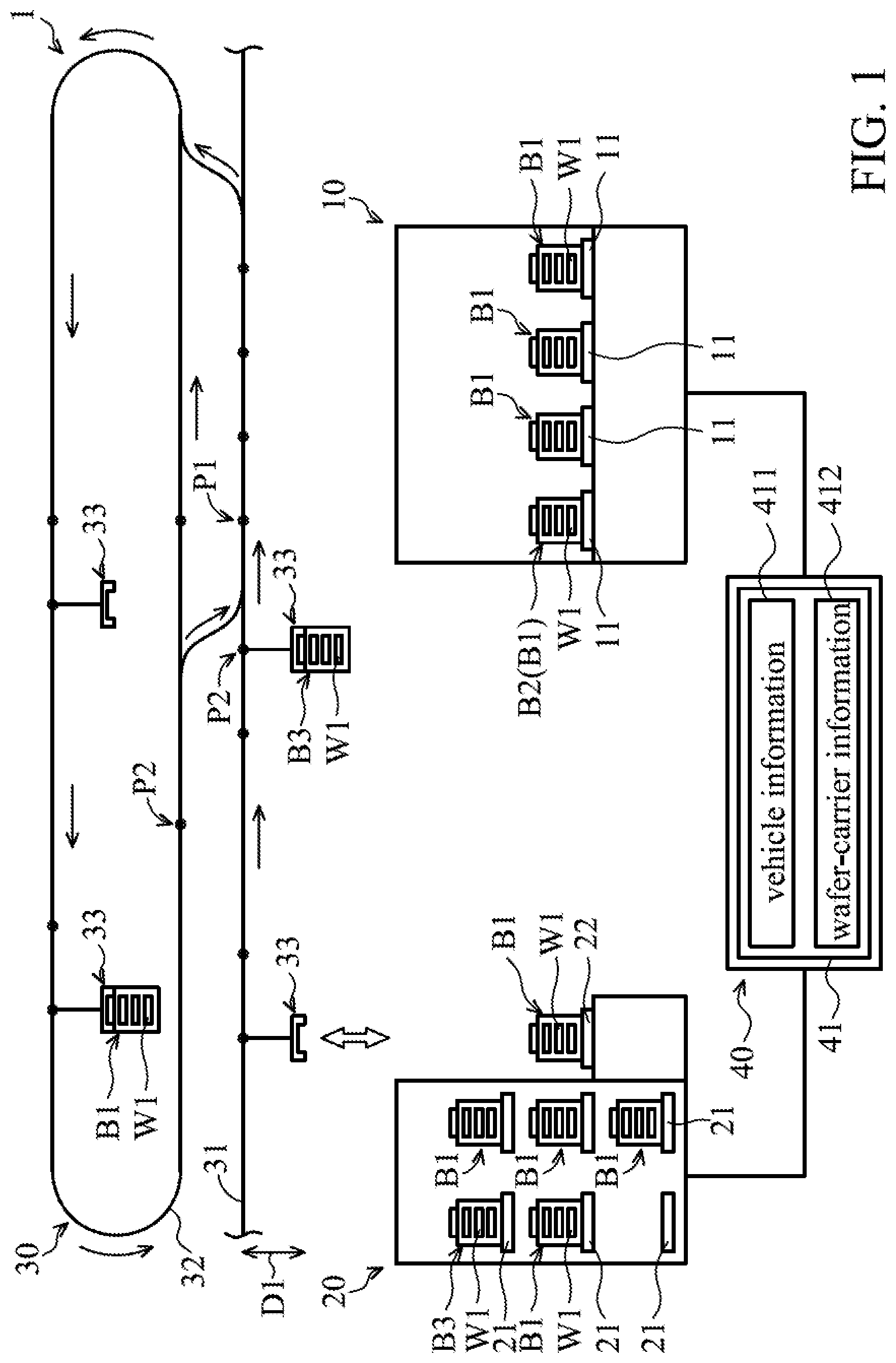
is a schematic view of a transport system 1 in accordance with some embodiments of the disclosure. The transport system 1 includes a semiconductor apparatus 10 , a stocker 20 , an OHT (Over Hoist Transport) system 30 , and a control system 40 . The semiconductor apparatus 10 is configured to perform a semiconductor manufacturing process on wafers W 1 .
In some embodiments, the semiconductor apparatus 10 includes a chemical mechanical polishing (CMP) apparatus, a physical vapor deposition (PVD) apparatus, a chemical vapor deposition (CVD) apparatus, an ion implant apparatus, an epitaxy apparatus, a sputter apparatus, a thermal processing apparatus, an etching apparatus, a photolithography apparatus, or another suitable apparatus. In some embodiments, the semiconductor manufacturing process includes a CMP process, a PVD process, a CVD process, an ALD process, a doping process, a screen printing process, a dry etching process, a wet etching process, a photolithography process, or another suitable processes.
The semiconductor apparatus 10 includes a number of load ports 11 . The load ports 11 are configured to load wafer carriers B 1 . In general, the semiconductor apparatus 10 includes, but not limited to, one to four load wafer carriers B 1 . The wafer carriers B 1 are configured to contain wafers W 1 . In some embodiments, some of the wafer carriers B 1 are empty wafer carriers without containing any wafers. In some embodiments, the wafer carrier is a wafer pod, a front opening unified pod (FOUP), a wafer lot, a wafer cassette, or a wafer boat.
When the wafer carrier B 1 is loaded at the load port 11 , the semiconductor apparatus 10 takes one or more wafers W 1 at the same time from the wafer carrier B 1 . After the wafer W 1 is processed by the semiconductor apparatus 10 , the wafer W 1 is put back into the wafer carrier B 1 .
The stocker 20 is configured to store a number of wafer carriers B 1 . The stocker 20 includes a number of support bases 21 inside the stocker 20 and a number of gate ports (load ports) 22 . The gate ports 22 are configured to load the wafer carriers B 1 . When the wafer carrier B 1 needs to be stored in the stocker 20 , the wafer carrier B 1 is to be loaded at the gate port 22 first, and afterward the stocker 20 transports the wafer carrier B 1 loaded at the gate port 22 to one of the support bases 21 . When one of the wafer carriers B 1 inside the stocker 20 needs to be transported to the semiconductor apparatus 10 , the stocker 20 transports the wafer carrier B 1 loaded at the support base 21 to the gate port 22 . Afterward, the OHT system 30 takes the wafer carrier B 1 from the gate port 22 and transports the wafer carrier B 1 to the semiconductor apparatus 10 .
The OHT system 30 includes a number of main tracks 31 , a number of circular tracks 32 and a number of vehicles 33 . In the , only one main track 31 and one circular track 32 are illustrated for clarity. The circular track 32 is connected at the main track 31 . The vehicle 33 is moveable along the main track 31 and the circular track 32 . The vehicle 33 is configured to transport one of the wafer carriers B 1 . In some embodiments, the vehicle 33 transports the wafer carrier B 1 from the stocker 20 to the semiconductor apparatus 10 , or from the semiconductor apparatus 10 to the stocker 20 .
Furthermore, the vehicle 33 is able to move along a vertical direction D 1 . In some embodiments, the vehicle 33 moves downwardly to attach the wafer carrier B 1 loaded at the load port 11 or the gate port 22 , and then the vehicle 33 hoists the wafer carrier B 1 to a position close to the main track 31 . The vehicle 33 with the wafer carrier B 1 moves along the main track 31 and/or the circular track 32 . In some embodiments, the vehicle 33 moves downwardly to put the wafer carrier B 1 at the load port 11 or the gate port 22 , and then the vehicle 33 detaches the wafer carrier B 1 . Afterward, the vehicle 33 leaves form the wafer carrier B 1 and rises up to back to the position close to the main track 31 .
The control system 40 is coupled with the semiconductor apparatus 10 , the stocker 20 , and the OHT system 30 . The control system 40 is configured to control the stocker 20 and the vehicle 33 . In some embodiments, the control system 40 is a wafer logistics system. In some embodiments, the control system 40 is a computer. The control system 40 includes a database 41 storing units of vehicle information 411 and units of wafer-carrier information 412 . Each unit of the vehicle information 411 corresponds to one of the vehicles 33 , and each unit of the wafer-carrier information 412 corresponds to one of the wafer carriers B 1 .
is a flow chart of a transport method in accordance with some embodiments of the disclosure. is a timing chart of the transport method in accordance with some embodiments of the disclosure.
In step S 101 , each of the load ports 11 loads one wafer carrier B 1 as shown in . In some embodiments, one of the wafer carriers B 1 loaded at the load ports 11 is assigned as a processing wafer carrier B 2 as shown in .
In some embodiments, the processing wafer carrier B 2 contains a number of wafers W 1 . When the processing wafer carrier B 2 is loaded at the load port 11 , the semiconductor apparatus 10 obtains the wafer-carrier information 412 corresponding to the processing wafer carrier B 2 . In some embodiments, each unit of the wafer-carrier information 412 includes wafer carrier ID (identification code) and units of wafer data. Each unit of the wafer data corresponds to one of the wafers W 1 contained in the wafer carrier B 1 .
In some embodiments, the semiconductor apparatus 10 obtains a wafer carrier ID from the processing wafer carrier B 2 . The semiconductor apparatus 10 transmits a wafer carrier-information request signal to the control system 40 . The control system 40 searches and selects one unit of the wafer-carrier information 412 that corresponds to the wafer carrier ID from the database 41 . Afterward, the control system 40 transmits the wafer-carrier information 412 that corresponds to the wafer carrier ID to the semiconductor apparatus 10 .
In step S 103 , the semiconductor apparatus 10 estimates a processed time T 4 according to the wafer data of the wafer-carrier information 412 . In some embodiments, the processed time T 4 is defined as a point of the time that the wafers W 1 of the processing wafer carrier B 2 have been processed by the semiconductor apparatus 10 .
In some embodiments, the semiconductor apparatus 10 finds out a recipe corresponding to the wafer data of the wafer-carrier information 412 . The recipe defines the processes that the semiconductor apparatus 10 performs on the wafers W 1 and the periods of the processes. The semiconductor apparatus 10 estimates the processed time T 4 and/or a process period E 1 according to the recipe, the number of wafers and the processed times of other wafer carriers B 1 loaded at the load ports 11 . In some embodiments, a process period E 1 is defined as the period between the time at which the processing wafer carrier B 2 is loaded at the load port 11 and the processed time T 4 .
In step S 105 , the semiconductor apparatus 10 transmits a request signal to the control system 40 at a request time T 1 . In some embodiments, the processing wafer carrier B 2 is loaded at the load port 11 at about the request time T 1 . In some embodiments, a process period E 1 is defined as the period between the request time T 1 and the processed time T 4 . The request time T 1 is earlier than the processed time T 4 by about the process period E 1 as shown in .
In some embodiments, the request signal includes an apparatus ID (identification code), the processed time T 4 , and a request condition. The apparatus ID corresponds to the semiconductor apparatus 10 . The request condition defines the characteristics of the semiconductor apparatus 10 , and/or the request for wafers W 1 proceeded by the semiconductor apparatus 10 .
For example, the request condition includes process data. The process data corresponds to a semiconductor manufacturing process that the semiconductor apparatus 10 performs on the wafer. In some embodiments, the request condition includes wafer-type data about what type of the wafers W 1 can be processed by the semiconductor apparatus 10 .
In step S 107 , the control system 40 receives the request signal and assigns one of the wafer carriers B 1 as an assigned wafer carrier B 3 (as shown in ) according to the request signal. In some embodiments, the control system 40 searches and finds out some units of the wafer-carrier information 412 matching the request condition of the request signal. Furthermore, the control system 40 selects the most suitable one from the units of the wafer-carrier information 412 selected by the control system 40 according to a judgment condition.
In some embodiments, the wafer-carrier information 412 further includes priority data and a quality time (Q-time). The judgment condition is that the control system 40 selects the most suitable one from the units of the wafer-carrier information 412 from the database 41 according to the priority data and/or the quality time.
In step 109 , the control system 40 controls the stocker 20 or the vehicle 33 starting to transport the assigned wafer carrier B 3 to the semiconductor apparatus 10 at a start time T 2 , which is earlier than the processed time T 4 . Since the assigned wafer carrier B 3 is transported before the wafers 11 of the processing wafer carrier B 2 are processed, a waiting period between the processed time T 4 and the delivery time T 5 is shortened. Therefore, the production rate of the semiconductor apparatus 10 is increased. Moreover, since the delivery time T 5 is early, the assigned wafer carrier B 3 can be processed by the semiconductor apparatus 10 in Q-time. Therefore, the yield of the wafers W 1 of the assigned wafer carrier B 3 is improved.
The control system 40 estimates a detaching period E 2 . The processing wafer carrier B 2 is detached from the load port 11 of the semiconductor apparatus 10 during the detaching period E 2 . The control system 40 estimates a delivery time T 5 at which the assigned wafer carrier B 3 is loaded at the load port 11 of the semiconductor apparatus 10 according to the processed time T 4 and the detaching period E 2 . In some embodiments, the delivery time T 5 is later than the processed time T 4 by about the detaching period E 2 . Thus, the delivery time T 5 is determined according to the processed time T 4 plus the detaching period E 2 .
In some embodiments, the control system 40 controls one of the vehicles 33 to transport the processing wafer carrier B 2 away from the semiconductor apparatus 10 at about the processed time T 4 . In some embodiments, the detaching period E 2 is in a range from about 6 seconds to about 10 seconds. Since the detaching period E 2 is short, the processed time T 4 is almost the same as the delivery time T 5 .
In some embodiments, the assigned wafer carrier B 3 is stored in the stocker 20 . The control system 40 plans a transport path, and then the assigned wafer carrier B 3 is transported from the stocker 20 to the load port 11 of the semiconductor apparatus 10 . Afterward, the control system 40 estimates a transport period E 3 according to a transport path. In some embodiments, the transport period E 3 is defined as a period during which the assigned wafer carrier B 3 is transported from the stocker 20 to the load port 11 of the semiconductor apparatus 10 . Therefore, in some embodiments, the start time T 2 is determined according to the processed time T 4 or the delivery time T 5 minus the transport period E 3 .
The start time T 2 is earlier than the delivery time T 5 or the processed time T 4 by about the transport period E 3 or less. In some embodiments, the process period E 1 is larger than the transport period E 3 estimated by the control system 40 . The start time T 2 is earlier than the processed time T 4 by about the process period E 1 or less.
In some embodiments, the transport period E 3 includes a stocker period E 4 and an OHT period E 5 . The control system 40 estimates the stocker period E 4 according to the time it takes for the assigned wafer carrier B 3 to be transported from the inside of the stocker 20 to the gate port 22 of the stocker 20 . The control system 40 estimates the OHT period E 5 according to the time it takes for the assigned wafer carrier B 3 to be transported from the gate port 22 of the stocker 20 to the load port 11 of the semiconductor apparatus 10 . Thus, the OHT period E 5 is defined as the period during which the assigned wafer carrier B 3 is transported by the vehicle 33 .
In some embodiments, the start time T 2 is earlier than the processed time T 4 by about the stocker period E 4 or greater. In some embodiments, the start time T 2 is earlier than the processed time T 4 by about the OHT period E 5 or greater.
In some embodiments, when the transport period E 3 estimated by the control system 40 is longer than the processed time T 4 , the control system 40 starts to transport the assigned wafer carrier B 3 to the semiconductor apparatus 10 immediately. Alternately, the control system 40 chooses to assign another wafer carrier B 1 as an assigned wafer carrier.
A to 4 C are schematic views of the transport system 1 during intermediate stages of the transport method. In step S 111 , the assigned wafer carrier B 3 is transported toward an elevation position P 1 of the main track 31 .
As shown in , 3 and 4 A , the assigned wafer carrier B 3 is transported from the support base 21 inside of the stocker 20 to the gate port 22 of the stocker 20 during the stocker period E 4 . The assigned wafer carrier B 3 is transported from the gate port 22 toward an elevation position P 1 of the main track 31 above the load port 11 by the vehicle 33 during the OHT period E 5 as shown in B .
In some embodiments, as shown in A , the vehicle 33 moves downwardly to attach the assigned wafer carrier B 3 at a departing time T 3 , and the vehicle 33 moves upwardly to the main track 31 with the assigned wafer carrier B 3 . Afterward, as shown in B , the vehicle 33 moves along the main track 31 with the assigned wafer carrier B 3 at a check position P 2 and toward the elevation position P 1 . The check position P 2 is prior to and close to the elevation position P 1 . In some embodiments, the check position P 2 is located at the circular track 32 .
In some embodiments, when the vehicle 33 with the assigned wafer carrier B 3 is located at the check position P 2 or the elevation position P 1 , the control system 40 checks whether the processing wafer carrier B 2 is loaded at the load port 11 .
In some embodiments, the vehicle 33 with the assigned wafer carrier B 3 is located at the check position P 2 and the processing wafer carrier B 2 is loaded at the load port 11 , as shown in B . The assigned wafer carrier B 3 is transported from the main track 31 to the circular track 32 when a priority value of the assigned wafer carrier B 3 is lower than a priority value of a following wafer carrier B 4 , as shown in B . Therefore, the following wafer carrier B 4 having a higher priority value can be processed early.
In some embodiments, the assigned wafer carrier B 3 is transported the assigned wafer carrier B 3 to the circular track 32 when the quality time (Q-time) of the assigned wafer carrier B 3 is longer than the quality time of a following wafer carrier B 4 as shown in B . Therefore, the following wafer carrier B 4 having a shorter quality time can be processed in time.
Afterward, the assigned wafer carrier B 3 is transported from the circular track 32 to toward the elevation position P 1 . Therefore, when the assigned wafer carrier B 3 is back to the check position P 2 or the elevation position P 1 again and the processing wafer carrier B 2 is still loaded at the load port 11 , the control system may control the vehicle 33 with the assigned wafer carrier B 3 to move to the circular track 32 again. Alternatively, the control system controls the vehicle 33 to transport the assigned wafer carrier B 3 to the stocker 20 or another semiconductor apparatus
In some embodiments, the vehicle 33 with the assigned wafer carrier B 3 is located at the check position P 2 , and the processing wafer carrier B 2 is loaded at the load port 11 . The assigned wafer carrier B 3 is stopped at the check position P 2 to wait for the processing wafer carrier B 2 to be transported away from the semiconductor apparatus 10 when the quality time of the assigned wafer carrier B 3 is less than a predetermined value. The predetermined value may be a value of a period during which the assigned wafer carrier B 3 is transported from the check position P 2 to the load port 11 via the circular track 32 . Therefore, the assigned wafer carrier B 3 having a short quality time can be processed in time.
In some embodiments, the assigned wafer carrier B 3 is stopped at the check position P 2 to wait for the processing wafer carrier B 2 to be transported away from the semiconductor apparatus 10 when the quality time of the assigned wafer carrier B 3 is shorter than the quality time of a following wafer carrier B 4 . Therefore, the assigned wafer carrier B 3 having a shorter quality time can be processed in time.
In some embodiments, the assigned wafer carrier B 3 is stopped at the check position P 2 to wait for the processing wafer carrier B 2 to be transported away from the semiconductor apparatus 10 when the priority value of the assigned wafer carrier B 3 is greater than the priority value of the following wafer carrier B 4 . Therefore, the assigned wafer carrier B 3 having a higher priority value can be processed early.
In some embodiments, the vehicle 33 with the assigned wafer carrier B 3 is located at the elevation position P 1 , and the processing wafer carrier B 2 is loaded at the load port 11 of the semiconductor apparatus 10 . The assigned wafer carrier B 3 is transported to the circular track 32 by the vehicle 33 . Afterward, the assigned wafer carrier B 3 is transported from the circular track 32 to back to the elevation position P 1 .
In some embodiments, the semiconductor apparatus 10 may be shut down during the transportation of the assigned wafer carrier B 3 . In this situation, the control system 40 may control the vehicle 33 to transport the assigned wafer carrier B 3 to the stocker 20 or another semiconductor apparatus.
In step S 113 , the processing wafer carrier B 2 is detached from the load port 11 by the vehicle 33 at the process time. The processing wafer carrier B 2 is transported away from the semiconductor apparatus 10 by the vehicle 33 during the detaching period E 2 .
In step S 115 , the vehicle 33 moves downwardly to put the assigned wafer carrier B 3 at the load port 11 . Afterward, the assigned wafer carrier B 3 is loaded at the load port 11 at about the delivery time T 5 , as shown in C . Since the assigned wafer carrier B 3 is transported at about the delivery time T 5 , a waiting period between the processed time T 4 and the delivery time T 5 is shortened. Therefore, the production rate of the semiconductor apparatus 10 is increased.
is a flow chart of a transport method in accordance with some embodiments of the disclosure. A to 6 C are schematic views of the transport system 1 during intermediate stages of the transport method.
As shown in A , the transport system 1 further includes a stocker 50 . The stocker 50 is configured to store wafer carriers, especially empty wafer carriers B 5 . The stocker 50 includes a number of support bases 51 inside the stocker 50 and gate ports 52 .
As shown in A , the processing wafer carrier B 2 is loaded on the load port 11 , and an emptied processing wafer carrier B 6 is loaded on the load port 11 . The processing wafer carrier B 2 includes a number of wafers W 1 . In this case, when the wafer W 1 is processed by the semiconductor apparatus 10 , the processed wafer W 1 is put into the processing emptied processing wafer carrier B 6 , rather than the processing wafer carrier B 2 .
In step S 201 , the wafer-carrier information 412 corresponding to the processing wafer carrier B 2 loaded at the load port 11 is obtained by the semiconductor apparatus 10 . In step S 203 , a processed time is estimated according to the wafer-carrier information 412 by the semiconductor apparatus 10 . In step S 205 , the semiconductor apparatus 10 transmits a request signal that includes the processed time to the control system 40 .
In step S 207 , the control system 40 assigns one of the wafer carriers B 1 as an assigned wafer carrier B 3 and assigns one of the empty wafer carriers B 5 as an assigned empty wafer carrier B 7 according to the request signal. In some embodiments, the assigned wafer carrier B 3 is stored in the stocker 20 , and the assigned empty wafer carrier B 7 is stored in the stocker 50 . In some embodiments, the assigned wafer carrier B 3 and the assigned empty wafer carrier B 7 are stored in the same stocker 20 or 50 .
In step S 209 , the control system 40 starts to control the stocker 20 and one of the vehicles 33 to transport the assigned wafer carrier B 3 to the semiconductor apparatus 10 at a first start time, which is earlier than the processed time. The control system 40 also starts to control the stocker 50 and one of the vehicles 33 to transport the assigned empty wafer carrier B 7 to the semiconductor apparatus 10 at a second start time, which is earlier than the processed time.
In step S 211 , the assigned wafer carrier B 3 is transported toward the elevation position P 1 of the main track 31 above the load port 11 by the vehicle 33 . The assigned empty wafer carrier B 7 is transported toward another elevation position P 1 of the main track 31 above another load port 11 by the vehicle 33 .
In step S 213 , the wafers W 1 in the processing wafer carrier B 2 are processed by the semiconductor apparatus 10 , and the processed wafers W 1 is put into the empty wafer carrier B 5 at the processed time. Therefore, the empty wafer carrier B 5 becomes a filled wafer carrier B 8 (as shown in B ). When the wafers W 1 are processed, the control system 40 controls two vehicles 33 to transport the processing wafer carrier B 2 and the filled wafer carrier B 8 away from the semiconductor apparatus 10 during a detaching time as shown in B .
In step S 215 , as shown in C , the control controls two vehicles 33 to load the assigned wafer carrier B 3 and the assigned empty wafer carrier B 7 at different load ports 11 of the semiconductor apparatus 10 .
Embodiments of transport systems and transport methods are provided. Since an assigned wafer carrier is transported before the wafers of a processing wafer carrier loaded at a semiconductor apparatus are processed, the waiting period between the time at which the wafers of the processing wafer carrier are processed and the time at which the assigned wafer carrier is delivered to the semiconductor apparatus is shortened. Therefore, the production rate of the semiconductor apparatus is increased. Moreover, since the assigned wafer carrier is delivered to the semiconductor apparatus earlier, the assigned wafer carrier can be processed by the semiconductor apparatus at the Q-time. Therefore, the yield of the wafers W 1 of the assigned wafer carrier B 3 is improved.
In some embodiments, a transport system is provided. The transport system includes a semiconductor apparatus configured to process a wafer and transmit a request signal at a request time. The request signal includes a processed time according to a processing wafer carrier loaded on a load port thereof. The processed time is defined as an estimated point of time according to the request time plus a process period, which is defined as an estimated period during which a plurality of wafers of the processing wafer carrier are processed by the semiconductor apparatus. The transport system also includes a vehicle configured to transport an assigned wafer carrier to the semiconductor apparatus along a transport path. The transport system further includes a control system configured to control the vehicle. When the control system receives the request signal, the control system estimates a delivery time according to the processed time plus a detaching period, estimates a transport period during which the assigned wafer carrier is transported along the transport path to the load port, and estimates a start time according to the delivery time minus the transport period. The delivery time is an estimated time when the assigned wafer carrier is loaded at the load port at a time later than the processed time and when the processing wafer carrier has been detached from the load port during the detaching period. The control system controls the vehicle to start transporting the assigned wafer carrier at the start time, which is earlier than the processed time.
In some embodiments, a transport method is provided. The transport method includes loading a processing wafer carrier at a load port of a semiconductor apparatus at a request time, wherein the processing wafer carrier contains a plurality of wafers. The transport method also includes estimating a processed time according to the processing wafer carrier by the semiconductor apparatus, wherein the processed time is defined as an estimated point of time according to the request time plus a process period, which is defined as an estimated period during which the plurality of wafers of the processing wafer carrier are processed by the semiconductor apparatus. The transport method also includes transmitting a request signal comprising the processed time to a control system by the semiconductor apparatus at the request time. The transport method further includes assigning an assigned wafer carrier according to the request signal, and estimating a delivery time according to the processed time plus a detaching period by the control system. The delivery time is an estimated time when the assigned wafer carrier is loaded at the load port at a time later than the processed time and when the processing wafer carrier has been detached from the load port during the detaching period. The transport method further includes estimating a transport period during which the assigned wafer carrier is transported along a transport path to the load port, and estimating a start time according to the delivery time minus the transport period by the control system. In addition, the transport method includes starting to transport the assigned wafer carrier to the semiconductor apparatus at the start time, which is earlier than the processed time.
In some embodiments, a transport method is provided. The transport method includes loading a processing wafer carrier at a load port of a semiconductor apparatus, wherein the processing wafer carrier contains a plurality of wafers. The transport method also includes estimating a processed time according to the processing wafer carrier by the semiconductor apparatus, wherein the processed time is defined as an estimated point of time that the plurality of wafers of the processing wafer carrier will be processed by the semiconductor apparatus. The transport method also includes transmitting a request signal comprising the processed time to a control system by the semiconductor apparatus at a request time. The transport method further includes assigning an assigned wafer carrier according to the request signal, and estimating a delivery time according to the processed time plus a detaching period by the control system. The delivery time is an estimated time when the assigned wafer carrier is loaded at the load port at a time later than the processed time and when the processing wafer carrier has been detached from the load port during the detaching period. The transport method further includes estimating a transport period during which the assigned wafer carrier is transported along a transport path to the load port, and estimating a start time according to the delivery time minus the transport period by the control system. In addition, the transport method includes starting to transport the assigned wafer carrier to the load port of the semiconductor apparatus at the start time, which is earlier than the processed time and later than the request time.
The foregoing outlines features of several embodiments so that those skilled in the art may better understand the aspects of the present disclosure. Those skilled in the art should appreciate that they may readily use the present disclosure as a basis for designing or modifying other processes and structures for carrying out the same purposes and/or achieving the same advantages of the embodiments introduced herein. Those skilled in the art should also realize that such equivalent constructions do not depart from the spirit and scope of the present disclosure, and that they may make various changes, substitutions, and alterations herein without departing from the spirit and scope of the present disclosure.
Figures (10)
Citations
This patent cites (38)
- US5329732
- US5980183
- US6577913
- US6745093
- US7068351
- US7195407
- US8204617
- US8483866
- US9606532
- US10042356
- US20020011203
- US20030013285
- US20060039781
- US20060190118
- US20060201375
- US20070185604
- US20080015723
- US20080275582
- US20090088895
- US20090226294
- US20100185305
- US20100278622
- US20110082579
- US20130079913
- US20140018955
- US20140067110
- US20140068753
- US20140099176
- US20140277668
- US20150162180
- US20150162228
- US20150212517
- US20160126120
- US20160276194
- US20160293461
- US20180282076
- US20190250594
- US20190258231