Display Panel and Manufacturing Method Thereof, and Display Device
Abstract
A display panel includes a base substrate and a plurality of sub-pixel groups. The plurality of sub-pixel groups includes a first sub-pixel group and a second sub-pixel group. The first sub-pixel group includes two adjacent sub-pixels with a first interval therebetween, and the second sub-pixel group includes two adjacent sub-pixels with a second interval therebetween. The first interval is different from the second interval.
Claims (8)
1. A display panel, comprising: a base substrate; and a plurality of sub-pixel groups disposed on the base substrate and arranged along a first direction, each of the plurality of sub-pixel groups comprising: a plurality of sub-pixels arranged along a second direction, the second direction intersecting the first direction; wherein the plurality of sub-pixel groups comprises a first sub-pixel group and a second sub-pixel group which are adjacent to each other, the first sub-pixel group comprising two adjacent sub-pixels with a first interval therebetween, and the second sub-pixel group comprising two adjacent sub-pixels with a second interval therebetween, the first interval being different from the second interval; the sub-pixels in the plurality of sub-pixel groups are capable of being divided into a plurality of pixels, each of the pixels comprises a plurality of sub-pixels, and two adjacent pixels have a gap in the second direction; a connecting line between two of the plurality of sub-pixels comprised in each of the pixels intersects both the first direction and the second direction; each of the pixels comprises a first sub-pixel, a second sub-pixel, a third sub-pixel, and a fourth sub-pixel; wherein the first sub-pixel and the second sub-pixel are arranged along the first direction; and the third sub-pixel and the fourth sub-pixel are on both sides of the first sub-pixel respectively, and the third sub-pixel, the first sub-pixel, and the fourth sub-pixel are arranged along the second direction; the plurality of sub-pixel groups further comprises a third sub-pixel group adjacent to the second sub-pixel group, the third sub-pixel group comprising two adjacent sub-pixels with a third interval therebetween, the third interval being different from the second interval; the first sub-pixel group comprises: a plurality of first sub-pixels, a plurality of third sub-pixels, and a plurality of fourth sub-pixels, the second sub-pixel group comprises: a plurality of first sub-pixels, a plurality of second sub-pixels, a plurality of third sub-pixels, and a plurality of fourth sub-pixels, and the third sub-pixel group comprises: a plurality of second sub-pixels; and the third interval is greater than the first interval, and the first interval is greater than the second interval.
6. A method of manufacturing a display panel, comprising: providing a base substrate; and forming a plurality of sub-pixel groups arranged along a first direction on the base substrate; wherein each of the plurality of sub-pixel groups comprises: a plurality of sub-pixels arranged along a second direction, and the second direction intersects the first direction; and the plurality of sub-pixel groups comprises a first sub-pixel group and a second sub-pixel group which are adjacent to each other, the first sub-pixel group comprising two adjacent sub-pixels with a first interval therebetween, and the second sub-pixel group comprising two adjacent sub-pixels with a second interval therebetween, the first interval being different from the second interval; the sub-pixels in the plurality of sub-pixel groups are capable of being divided into a plurality of pixels, each of the pixels comprises a plurality of sub-pixels, and two adjacent pixels have a gap in the second direction; a connecting line between two of the plurality of sub-pixels comprised in each of the pixels intersects both the first direction and the second direction; each of the pixels comprises a first sub-pixel, a second sub-pixel, a third sub-pixel, and a fourth sub-pixel; wherein the first sub-pixel and the second sub-pixel are arranged along the first direction; and the third sub-pixel and the fourth sub-pixel are on both sides of the first sub-pixel respectively, and the third sub-pixel, the first sub-pixel, and the fourth sub-pixel are arranged along the second direction; the plurality of sub-pixel groups further comprises a third sub-pixel group adjacent to the second sub-pixel group, the third sub-pixel group comprising two adjacent sub-pixels with a third interval therebetween, the third interval being different from the second interval; the first sub-pixel group comprises: a plurality of first sub-pixels, a plurality of third sub-pixels, and a plurality of fourth sub-pixels, the second sub-pixel group comprises: a plurality of first sub-pixels, a plurality of second sub-pixels, a plurality of third sub-pixels, and a plurality of fourth sub-pixels, and the third sub-pixel group comprises: a plurality of second sub-pixels; and the third interval is greater than the first interval, and the first interval is greater than the second interval.
7. A display device, comprising: a drive circuit and a display panel; wherein the display panel comprises: a base substrate; and a plurality of sub-pixel groups disposed on the base substrate and arranged along a first direction, wherein each of the plurality of sub-pixel groups comprises: a plurality of sub-pixels arranged along a second direction, and the second direction intersects the first direction; and the plurality of sub-pixel groups comprises a first sub-pixel group and a second sub-pixel group which are adjacent to each other, the first sub-pixel group comprising two adjacent sub-pixels with a first interval therebetween, the second sub-pixel group comprising two adjacent sub-pixels with a second interval therebetween, the first interval being different from the second interval; and the drive circuit is connected to the plurality of sub-pixels, and the drive circuit is configured to provide drive signals for the plurality of sub-pixels; the sub-pixels in the plurality of sub-pixel groups are capable of being divided into a plurality of pixels, each of the pixels comprises a plurality of sub-pixels, and two adjacent pixels have a gap in the second direction; a connecting line between two of the plurality of sub-pixels comprised in each of the pixels intersects both the first direction and the second direction; each of the pixels comprises a first sub-pixel, a second sub-pixel, a third sub-pixel, and a fourth sub-pixel; wherein the first sub-pixel and the second sub-pixel are arranged along the first direction; and the third sub-pixel and the fourth sub-pixel are on both sides of the first sub-pixel respectively, and the third sub-pixel, the first sub-pixel, and the fourth sub-pixel are arranged along the second direction; the plurality of sub-pixel groups further comprises a third sub-pixel group adjacent to the second sub-pixel group, the third sub-pixel group comprising two adjacent sub-pixels with a third interval therebetween, the third interval being different from the second interval; the first sub-pixel group comprises: a plurality of first sub-pixels, a plurality of third sub-pixels, and a plurality of fourth sub-pixels, the second sub-pixel group comprises: a plurality of first sub-pixels, a plurality of second sub-pixels, a plurality of third sub-pixels, and a plurality of fourth sub-pixels, and the third sub-pixel group comprises: a plurality of second sub-pixels; and the third interval is greater than the first interval, and the first interval is greater than the second interval.
Show 5 dependent claims
2. The display panel according to claim 1 , wherein a length of each sub-pixel along the second direction is m; and the first interval, the second interval, and the third interval satisfy: h 3 −h 1 =2×m; h 1 =2×h 2 +m; h 3 =3×h 2 +m, wherein h 1 is the first interval, h 2 is the second interval, and h 3 is the third interval.
3. The display panel according to claim 2 , wherein the first interval is equal to the length of five sub-pixels along the second direction, the second interval is equal to the length of two sub-pixels along the second direction, and the third interval is equal to the length of seven sub-pixels along the second direction.
4. The display panel according to claim 1 , wherein a color of the first sub-pixel is one of red and blue, a color of the second sub-pixel is the other of red and blue, and a color of the third sub-pixel and a color of the fourth sub-pixel are both green.
5. The display panel according to claim 1 , wherein the first direction is a pixel column direction, and the second direction is a pixel row direction.
8. The display device according to claim 7 , further comprising: a plurality of drive lines, wherein one end of the drive line is connected to the drive circuit, and the other end of the drive line is connected to the plurality of sub-pixels; and an orthographic projection of the drive line on the base substrate is in an edge region of an orthographic projection of a gap between two adjacent sub-pixels with an interval therebetween on the base substrate.
Full Description
Show full text →
This application claims priority to Chinese Patent Application No. 202011074634.3, filed on Oct. 9, 2020 and entitled “DISPLAY PANEL AND DISPLAY DEVICE”, which is incorporated herein by reference in its entirety.
TECHNICAL FIELD
The present disclosure relates to the field of display technologies, and in particular to a display panel and a manufacturing method thereof, and a display device.
BACKGROUND
Transparent display panels have good transparency and can display images, and thus are widely used.
In the related art, the transparent display panel includes: a base substrate and a plurality of pixel columns disposed on the base substrate. There is no gap between the plurality of pixels included in each pixel column, there is a gap between two adjacent pixel columns, and external light can pass through the gap between the two adjacent pixel columns.
SUMMARY
The present disclosure provides a display panel and a manufacturing method thereof, and a display device. The technical solutions are as follows.
In an aspect, a display panel is provided. The display panel includes: a base substrate; and a plurality of sub-pixel groups disposed on the base substrate and arranged along a first direction, wherein the sub-pixel group includes: a plurality of sub-pixels arranged along a second direction, and the second direction intersects the first direction; wherein the plurality of sub-pixel groups includes a first sub-pixel group and a second sub-pixel group which are adjacent to each other, the first sub-pixel group includes two adjacent sub-pixels with a first interval therebetween, the second sub-pixel group includes two adjacent sub-pixels with a second interval therebetween, and the first interval is different from the second interval.
Optionally, the sub-pixels in the plurality of sub-pixel groups are divided into a plurality of pixels, the pixel includes a plurality of sub-pixels, and two adjacent pixels have a gap in the second direction.
Optionally, a connecting line between two of the plurality of sub-pixels included in the pixel intersects both the first direction and the second direction.
Optionally, the pixel includes a first sub-pixel, a second sub-pixel, a third sub-pixel, and a fourth sub-pixel; wherein the first sub-pixel and the second sub-pixel are arranged along the first direction; and the third sub-pixel and the fourth sub-pixel are disposed on both sides of the first sub-pixel respectively, and the third sub-pixel, the first sub-pixel, and the fourth sub-pixel are arranged along the second direction.
Optionally, the first sub-pixel group includes: a plurality of first sub-pixels, a plurality of third sub-pixels, and a plurality of fourth sub-pixels; and the second sub-pixel group includes: a plurality of second sub-pixels; wherein the first interval is smaller than the second interval.
Optionally, a length of each sub-pixel along the second direction is m, and the first interval and the second interval satisfy: h 2 −h 1 =2×m, wherein h 1 is the first interval, and h 2 is the second interval.
Optionally, the first interval is equal to the length of one sub-pixel along the second direction, and the second interval is equal to the length of three sub-pixels along the second direction.
Optionally, the first interval is equal to the length of two sub-pixels along the second direction, and the second interval is equal to the length of four sub-pixels along the second direction.
Optionally, the plurality of sub-pixel groups further includes a third sub-pixel group adjacent to the second sub-pixel group, the third sub-pixel group has two adjacent sub-pixels with a third interval therebetween, and the third interval is different from the second interval.
Optionally, the first sub-pixel group includes: a plurality of first sub-pixels, a plurality of third sub-pixels, and a plurality of fourth sub-pixels, the second sub-pixel group includes: a plurality of first sub-pixels, a plurality of second sub-pixels, a plurality of third sub-pixels, and a plurality of fourth sub-pixels, and the third sub-pixel group includes: a plurality of second sub-pixels; wherein the third interval is greater than the first interval, and the first interval is greater than the second interval.
Optionally, the length of each sub-pixel along the second direction is m; and the first interval, the second interval, and the third interval satisfy: h 3 −h 1 =2×m; h 1 =2×h 2 +m; h 3 =3×h 2 +m, wherein h 1 is the first interval, h 2 is the second interval, and h 3 is the third interval.
Optionally, the first interval is equal to the length of five sub-pixels along the second direction, the second interval is equal to the length of two sub-pixels along the second direction, and the third interval is equal to the length of seven sub-pixels along the second direction.
Optionally, the first sub-pixel group includes: a plurality of first sub-pixels, a plurality of third sub-pixels, and a plurality of fourth sub-pixels, the second sub-pixel group includes: a plurality of second sub-pixels, and the third sub-pixel group includes: a plurality of first sub-pixels, a plurality of third sub-pixels, and a plurality of fourth sub-pixels; wherein the third interval is equal to the first interval, and the first interval is greater than the second interval.
Optionally, the length of each sub-pixel along the second direction is m; and the first interval, the second interval, and the third interval satisfy: h 1 =h 3 =2×h 2 −m, wherein h 1 is the first interval, h 2 is the second interval, and h 3 is the third interval.
Optionally, the first interval is equal to the length of five sub-pixels along the second direction, the second interval is equal to the length of three sub-pixels along the second direction, and the third interval is equal to the length of five sub-pixels along the second direction.
Optionally, a color of the first sub-pixel is one of red and blue, a color of the second sub-pixel is the other of red and blue, and a color of the third sub-pixel and a color of the fourth sub-pixel are both green.
Optionally, the first direction is a pixel column direction, and the second direction is a pixel row direction.
In another aspect, a method of manufacturing a display panel is provided. The method includes: providing a base substrate; and forming a plurality of sub-pixel groups arranged along a first direction on the base substrate; wherein the sub-pixel group includes: a plurality of sub-pixels arranged along a second direction, and the second direction intersects the first direction; the plurality of sub-pixel groups includes a first sub-pixel group and a second sub-pixel group which are adjacent to each other, the first sub-pixel group has two adjacent sub-pixels with a first interval therebetween, the second sub-pixel group has two adjacent sub-pixels with a second interval therebetween, and the first interval is different from the second interval.
In yet another aspect, a display device is provided. The display device includes: a drive circuit and a display panel; wherein the display panel includes: a base substrate; and a plurality of sub-pixel groups disposed on the base substrate and arranged along a first direction, wherein the sub-pixel group includes: a plurality of sub-pixels arranged along a second direction, and the second direction intersects the first direction; the plurality of sub-pixel groups includes a first sub-pixel group and a second sub-pixel group which are adjacent to each other, the first sub-pixel group has two adjacent sub-pixels with a first interval, the second sub-pixel group has two adjacent sub-pixels with a second interval, and the first interval is different from the second interval; and the drive circuit is connected to the plurality of sub-pixels, and the drive circuit is configured to provide drive signals for the plurality of sub-pixels.
Optionally, the display device further includes: a plurality of drive lines, wherein one end of the drive line is connected to the drive circuit, and the other end of the drive line is connected to the plurality of sub-pixels; and an orthographic projection of the drive line on the base substrate is in an edge region of an orthographic projection of a gap between two adjacent sub-pixels with an interval on the base substrate.
BRIEF DESCRIPTION OF THE DRAWINGS
For clearer descriptions of the technical solutions in the embodiments of the present disclosure, the following briefly introduces the accompanying drawings required for describing the embodiments. The accompanying drawings in the following description show merely some embodiments of the present disclosure, and persons of ordinary skill in the art may still derive other drawings from these accompanying drawings without creative efforts.
is a schematic diagram of light intensity of single-slit diffraction according to an embodiment of the present disclosure;
is a schematic diagram of light intensity of multi-slit interference according to an embodiment of the present disclosure;
is a schematic structural diagram of a grating according to an embodiment of the present disclosure;
is a schematic diagram of light intensity of multi-slit diffraction according to an embodiment of the present disclosure;
is a schematic structural diagram of a transparent display panel in the related art;
is a schematic structural diagram of another transparent display panel in the related art;
is a schematic structural diagram of yet another transparent display panel in the related art;
is a simulation diagram of a diffraction effect of the transparent display panel shown in ;
is a simulation diagram of a diffraction effect of the transparent display panel shown in ;
is a simulation diagram of a diffraction effect of the transparent display panel shown in ;
is a schematic structural diagram of a display panel according to an embodiment of the present disclosure;
is a schematic structural diagram of another display panel according to an embodiment of the present disclosure;
is a schematic structural diagram of yet another display panel according to an embodiment of the present disclosure;
is a simulation diagram of a diffraction effect of the display panel shown in ;
is a simulation diagram of a diffraction effect of the display panel shown in ;
is a schematic structural diagram of still another display panel according to an embodiment of the present disclosure;
is a schematic structural diagram of still another display panel according to an embodiment of the present disclosure;
is a simulation diagram of a diffraction effect of the display panel shown in ;
is a schematic structural diagram of still another display panel according to an embodiment of the present disclosure;
is a simulation diagram of a diffraction effect of the display panel shown in ;
is a flowchart of a method of manufacturing a display panel according to an embodiment of the present disclosure;
is a schematic structural diagram of a display device according to an embodiment of the present disclosure; and
is a schematic diagram of a partial structure of a display device according to an embodiment of the present disclosure.
DETAILED DESCRIPTION
For clearer descriptions of the objectives, technical solutions, and advantages of the present disclosure, embodiments of the present disclosure are described in detail hereinafter with reference to the accompanying drawings.
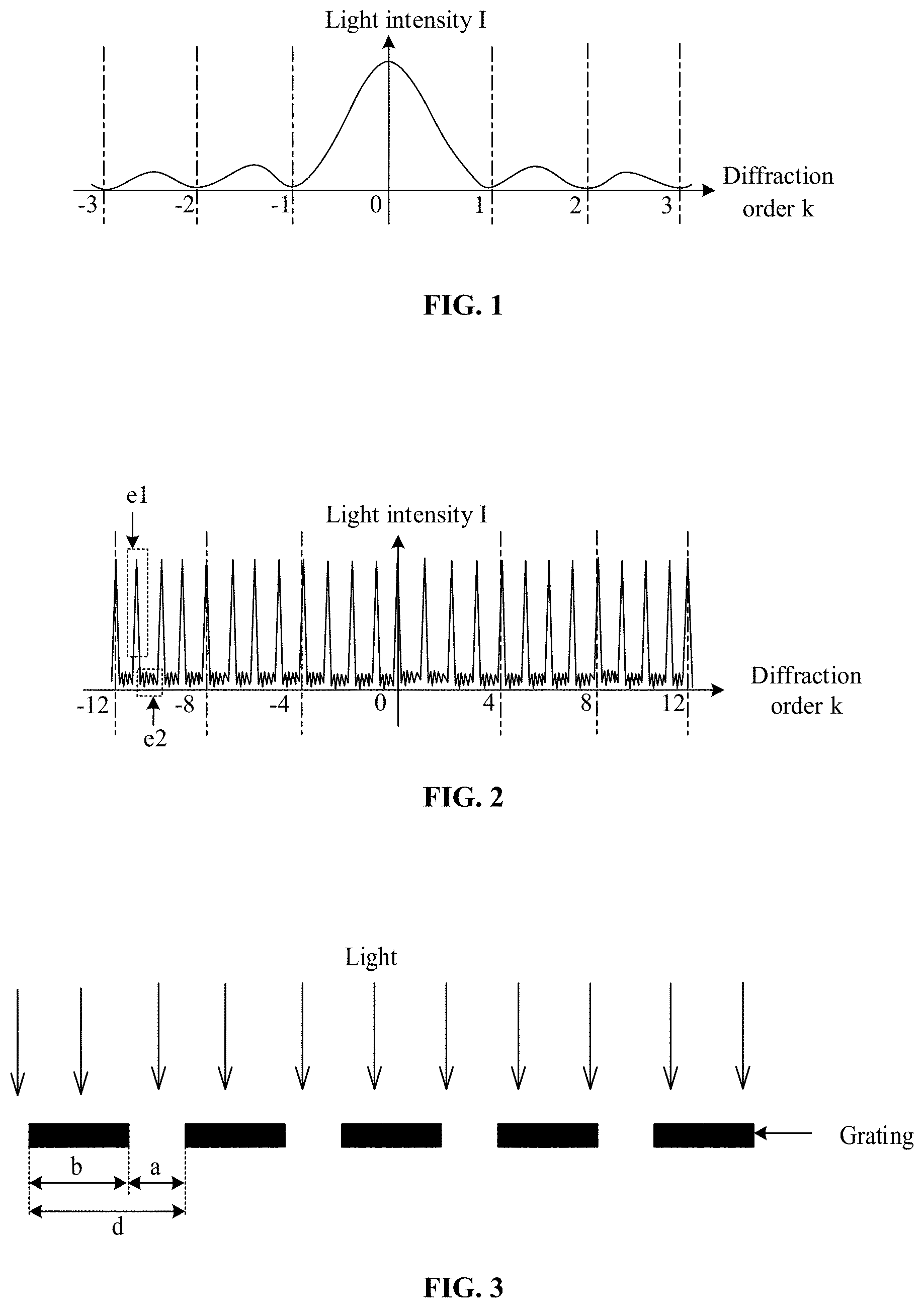
Single-slit diffraction is a phenomenon that light waves bypass an obstacle and continue to propagate when light encounters the obstacle during propagation. As shown in , in the single-slit diffraction, the smaller the absolute value of a diffraction order k is, the greater the light intensity I is; and the larger the absolute value of the diffraction order k is, the less the light intensity I is, where k may be an integer. Light interference is a phenomenon that two or more columns of light overlap each other when meeting in space, and the light is always intensified in some regions e 1 and always weakened in other regions e 2 , thereby forming a stable intensity-weakness distribution, as shown in .
is a schematic structural diagram of a grating according to an embodiment of the present disclosure. Referring to , the grating may be an optical element including a plurality of parallel slits with an equal width and equal interval. In , the width of a light-transmitting region (the light-transmitting region may also be called a slit) may be a, the width of an opaque region may be b, and the sum of the width of the light-transmitting region and the width of the opaque region may be called a length d of one period of the grating, that is, d=a+b.
The light intensity curve of multi-slit interference is shown in , and the light intensity of multi-slit interference satisfies:
I = I 0 ( sin α α ) 2 ( sin N β sin β ) 2 , Formula ( 1 ) where I 0 refers to an initial light intensity when the light irradiates the grating without bypassing the obstacle to continue to propagate.
sin α α may refer to a single-slit diffraction factor, and
sin N β sin β may refer to a multi-slit interference factor. α may satisfy:
α = π a sin θ λ . β may satisfy:
β = π d sin θ λ . θ may be a diffraction angle, λ is a wavelength of light, N is the number of light-transmitting regions, and N may be a positive integer greater than or equal to 1.
With reference to the above Formula (1), it can be seen that the single-slit diffraction is related to the width a of the light-transmitting region, and the multi-slit interference is related to the length d of one period of the grating. In addition, the multi-slit diffraction is a combined effect of the single-slit diffraction simultaneously generated by each single slit and the multi-light interference generated by parallel light diffracted by each single slit. The diffraction effect of the multi-slit diffraction can be reduced by reducing the width a of the light-transmitting region or increasing the length d of one period of the grating.
Optionally, a dark stripe of the single-slit diffraction satisfies: a×sin θ=±kλ, and a bright fringe of the multi-slit interference satisfies: d×sin θ=±kλ, where k is the diffraction order shown in to .
In the related art, referring to to , the transparent display panel includes: a plurality of pixel columns 001 . There is no gap between multiple pixels included in each pixel column 001 , and there is a gap between every two adjacent pixel columns 001 . The gap between every two adjacent pixel columns 001 may be a light-transmitting region, and light can pass through the gap between every two adjacent pixel columns. That is, the transparent display panel may be regarded as a grating composed of multiple light-transmitting regions.
The gap c 1 between two adjacent pixel columns 001 in is smaller than the gap c 2 between two adjacent pixel columns 001 in , and the gap c 2 between two adjacent pixel columns 001 in is smaller than the gap c 3 between two adjacent pixel columns 001 in . That is, the width of the light-transmitting region in the transparent display panel shown in is smaller than the width of the light-transmitting region in the transparent display panel shown in , and the width of the light-transmitting region in the transparent display panel shown in is smaller than the width of the light-transmitting region in the transparent display panel shown in .
The diffraction effect of the transparent display panel shown in is simulated as shown in , the diffraction effect of the transparent display panel shown in is simulated as shown in , and the diffraction effect of the transparent display panel shown in is simulated as shown in . It can be seen in conjunction with to that the ghost image of an image displayed on the transparent display panel shown in is more obvious than that of the image displayed on the transparent display panel shown in , and the ghost image of the image displayed on the transparent display panel shown in is more obvious than that of the image displayed on the transparent display panel shown in . That is, the diffraction effect of the transparent display panel shown in is stronger than that of the transparent display panel shown in , and the diffraction effect of the transparent display panel shown in is stronger than that of the transparent display panel shown in .
In the related art, by increasing the gap between adjacent pixel columns in the transparent display panel, the diffraction effect of the transparent display panel can be reduced. However, referring to , after increasing the gap between adjacent pixel columns in the transparent display panel, the ghost image of the image displayed on the transparent display panel is still obvious, and the display effect of the transparent display panel is poor.
The display panel according to an embodiment of the present disclosure can solve the problem of poor display effect of the display panel in the related art. Referring to , the display panel 10 may include: a base substrate 101 and a plurality of sub-pixel groups 102 . The plurality of sub-pixel groups 102 may be disposed on the base substrate 101 and arranged along a first direction A 1 . Four sub-pixel groups 102 are shown in . The sub-pixel group 102 may include a plurality of sub-pixels arranged along a second direction A 2 . The second direction A 2 intersects the first direction A 1 . For example, the second direction A 2 in may be perpendicular to the first direction A 1 .
Referring to , the plurality of sub-pixel groups 102 includes a first sub-pixel group 102 a and a second sub-pixel group 102 b which are adjacent to each other. The first sub-pixel group 102 a includes two adjacent sub-pixels (X 1 and X 2 ) with a first interval h 1 therebetween. The second sub-pixel group 102 b includes two adjacent sub-pixels (Y 1 and Y 2 ) with a second interval h 2 therebetween. The first interval h 1 is different from the second interval h 2 .
The interval between two sub-pixels included in the sub-pixel group may refer to the distance between the side of a first sub-pixel close to a second sub-pixel and the side of the second sub-pixel close to the first sub-pixel. Referring to , the first interval h 1 between the sub-pixel X 1 and the sub-pixel X 2 refers to the distance between the side of the sub-pixel X 1 close to the sub-pixel X 2 and the side of the sub-pixel X 2 close to the sub-pixel X 1 . The second interval h 2 between the sub-pixel Y 1 and the sub-pixel Y 2 refers to the distance between the side of the sub-pixel Y 1 close to the sub-pixel Y 2 and the side of the sub-pixel Y 2 close to the sub-pixel Y 1 .
In the embodiment of the present disclosure, the first interval h 1 between the two adjacent sub-pixels (X 1 and X 2 ) in the first sub-pixel group 102 a is different from the second interval h 2 between the two adjacent pixels (Y 1 and Y 2 ) in the second sub-pixel group 102 b , so the diffraction order of light passing through the gap between the two adjacent sub-pixels (X 1 and X 2 ) in the first sub-pixel group 102 a is different from the diffraction order of the light passing through the gap between the two adjacent sub-pixels (Y 1 and Y 2 ) in the second sub-pixel group 102 b . Therefore, the diffraction effect of the light emitting from the gap between adjacent sub-pixels can be reduced, and the display effect of the display panel 10 is better.
In summary, the embodiment of the present disclosure provides a display panel. In the display panel, the first sub-pixel group has two adjacent sub-pixels with the first interval, and the second sub-pixel group has two adjacent sub-pixels with the second interval. The first interval is different from the second interval, so that the diffraction order of the light passing through the gap between the two sub-pixels in the first sub-pixel group is different from that of the light passing through the gap between the two sub-pixels in the second sub-pixel group. Therefore, the diffraction effect can be reduced, and the display effect of the display panel is improved.
Optionally, the first direction A 1 may be a pixel column direction, and the second direction A 2 may be a pixel row direction. Certainly, the first direction A 1 may be a pixel row direction, and the second direction A 2 may be a pixel column direction, which is not limited in the embodiments of the present disclosure.
Referring to , it can be seen that the sub-pixels in the plurality of sub-pixel groups 102 may be divided into a plurality of pixels. Each pixel G may include a plurality of sub-pixels, and there is a gap between two adjacent pixels G in the second direction A 2 . Thus, there is a gap between two adjacent sub-pixels in the sub-pixel group 102 . The color of the combined light emitted from the plurality of sub-pixels included in each pixel may be white.
Optionally, in the plurality of sub-pixels included in the pixel G in the display panel 10 , there is a connecting line between two of the sub-pixels which intersects both the first direction A 1 and the second direction A 2 . That is, the plurality of sub-pixels included in the pixel G are not arranged in the same direction (the first direction A 1 or the second direction A 2 ). In addition, in the plurality of sub-pixels included in each pixel, at least two sub-pixels belong to different sub-pixel groups.
Referring to , it can be seen that each pixel G may include a first sub-pixel g 1 , a second sub-pixel g 2 , a third sub-pixel g 3 , and a fourth sub-pixel g 4 . That is, the pixel G may include four sub-pixels. The first sub-pixel g 1 and the second sub-pixel g 2 may be arranged along the first direction A 1 . The third sub-pixel g 3 and the fourth sub-pixel g 4 may be respectively disposed on both sides of the first sub-pixel g 1 , and the third sub-pixel g 3 , the first sub-pixel g 1 , and the fourth sub-pixel g 4 may be arranged along the second direction A 2 .
Referring to , for each pixel G, the connecting line between the second sub-pixel g 2 and the third sub-pixel g 3 , and the connecting line between the second sub-pixel g 2 and the fourth sub-pixel g 4 intersect both the first direction A 1 and the second direction A 2 . For each pixel G, the first sub-pixel g 1 , the second sub-pixel g 2 , the third sub-pixel g 3 , and the fourth sub-pixel g 4 may be arranged in a “T” shape.
Optionally, in the four sub-pixels included in the pixel G, the color of at least one sub-pixel is red (R), the color of at least one sub-pixel is green (G), and the color of at least one sub-pixel is blue (B).
Exemplarily, the color of the first sub-pixel g 1 may be one of red and blue, the color of the second sub-pixel g 2 may be the other of red and blue, and the color of the third sub-pixel g 3 and the color of the fourth sub-pixel g 4 may be both green. That is, in the four sub-pixels included in the pixel G, the color of one sub-pixel is red, the color of one sub-pixel is blue, and the color of the other two sub-pixels is green.
In the embodiment of the present disclosure, the pixel G may include less or more sub-pixels, which is not limited in the embodiment of the present disclosure, as long as the color of the combined light emitted from the plurality of sub-pixels included in the pixel G is white.
Referring to , it can be seen that the first sub-pixel group 102 a may include: a plurality of first sub-pixels g 1 , a plurality of third sub-pixels g 3 , and a plurality of fourth sub-pixels g 4 , and the second sub-pixel group 102 b may include: a plurality of second sub-pixels g 2 . The first interval h 1 may be smaller than the second interval h 2 .
In the embodiment of the present disclosure, referring to , the first pixel G 1 and the second pixel G 2 are adjacent to each other and are arranged along the second direction A 2 . The sub-pixels sequentially arranged along the second direction A 2 in the first sub-pixel group 102 a include: the third sub-pixel g 3 of the first pixel G 1 , the first sub-pixel g 1 of the first pixel G 1 , the fourth sub-pixel g 4 of the first pixel G 1 , the third sub-pixel g 3 of the second pixel G 2 , the first sub-pixel g 1 of the second pixel G 2 , and the fourth sub-pixel g 4 of the second pixel G 2 . Furthermore, the sub-pixels sequentially arranged along the second direction A 2 in the second sub-pixel group 102 b include: the second sub-pixel g 2 of the first pixel G 1 and the second sub-pixel g 2 of the second pixel G 2 .
The first pixel G 1 and the second pixel G 2 have a gap therebetween along the second direction A 2 . Referring to , the two adjacent sub-pixels with the first interval h 1 therebetween in the first sub-pixel group 102 a may include: the fourth sub-pixel g 4 of the first pixel G 1 and the third sub-pixel g 3 of the second pixel G 2 . That is, the fourth sub-pixel g 4 of the first pixel G 1 and the third sub-pixel g 3 of the second pixel G 2 have the first interval h 1 therebetween along the second direction A 2 .
In addition, the two adjacent sub-pixels with the second interval h 2 therebetween in the second sub-pixel group 102 b may include: the second sub-pixel g 2 of the first pixel G 1 and the second sub-pixel g 2 of the second pixel G 2 . That is, the second sub-pixel g 2 of the first pixel G 1 and the second sub-pixel g 2 of the second pixel G 2 have the second interval h 2 therebetween along the second direction A 2 .
In the embodiment of the present disclosure, the length of each sub-pixel included in the display panel 10 along the second direction A 2 may be the same. Referring to , the first interval h 1 may be equal to the length of one sub-pixel along the second direction A 2 , and the second interval h 2 may be equal to the length of three sub-pixels along the second direction A 2 . The white filling in or indicates that no sub-pixels are disposed.
Alternatively, referring to , the first interval h 1 may be equal to the length of two sub-pixels in the second direction A 2 , and the second interval h 2 may be equal to the length of four sub-pixels in the second direction A 2 .
The diffraction effect of the display panel shown in is simulated as shown in , and the diffraction effect of the display panel shown in is simulated as shown in . It can be seen in conjunction with and that the ghost image of the image displayed on the display panel shown in is more obvious than the ghost image of the image displayed on the display panel shown in . That is, the display panel shown in has a strong diffraction effect, and the display panel shown in has a weak diffraction effect.
The diffraction effect of the display panel 10 is negatively correlated with the first interval h 1 and the second interval h 2 . The larger the first interval h 1 and the second interval h 2 are, the weaker the diffraction effect of the display panel 10 is. The smaller the first interval h 1 and the second interval h 2 are, the stronger the diffraction effect of the display panel 10 is.
In the embodiment of the present disclosure, the first interval h 1 and the second interval h 2 may be equal to the length of other numbers of sub-pixels along the second direction A 2 , which is not limited in the embodiment of the present disclosure. However, if the arrangement of the pixels in the display panel is the same as the arrangement shown in and , and only the gap between adjacent pixels in the second direction A 2 is adjusted (that is, the sizes of the first interval h 1 and the second interval h 2 are adjusted), the difference between the second interval h 2 and the first interval h 1 may be equal to the length of two sub-pixels along the second direction A 2 .
That is, in the display panel 10 shown in and , the first interval h 1 and the second interval h 2 satisfy: h 2 −h 1 =2×m, where m is the length of one sub-pixel along the second direction A 2 .
is a schematic structural diagram of yet another display panel according to an embodiment of the present disclosure. It can also be seen with reference to that the plurality of sub-pixel groups 102 further includes a third sub-pixel group 102 c adjacent to the second sub-pixel group 102 b . The third sub-pixel group 102 c has two adjacent sub-pixels (Z 1 and Z 2 ) with a third interval h 3 therebetween. Since the third sub-pixel group 102 c is adjacent to the second sub-pixel group 102 b , the third interval h 3 is different from the second interval h 2 .
Referring to , it can be seen that the first sub-pixel group 102 a may include: a plurality of first sub-pixels g 1 , a plurality of third sub-pixels g 3 , and a plurality of fourth sub-pixels g 4 . The second sub-pixel group 102 b may include: a plurality of first sub-pixels g 1 , a plurality of second sub-pixels g 2 , a plurality of third sub-pixels g 3 , and a plurality of fourth sub-pixels g 4 . The third sub-pixel group 102 c may include: a plurality of second sub-pixels g 2 . The third interval h 3 may be greater than the first interval h 1 , and the first interval h 1 may be greater than the second interval h 2 .
In the embodiment of the present disclosure, referring to , the first pixel G 1 , the second pixel G 2 , the third pixel G 3 , and the fourth pixel G 4 are sequentially arranged along the second direction A 2 . The sub-pixels sequentially arranged along the second direction A 2 in the first sub-pixel group 102 a include: the third sub-pixel g 3 of the first pixel G 1 , the first sub-pixel g 1 of the first pixel G 1 , the fourth sub-pixel g 4 of the first pixel G 1 , the third sub-pixel g 3 of the third pixel G 3 , the first sub-pixel g 1 of the third pixel G 3 , and the fourth sub-pixel g 4 of the third pixel G 3 .
The sub-pixels sequentially arranged along the second direction A 2 in the second sub-pixel group 102 b include: the second sub-pixel g 2 of the first pixel G 1 , the third sub-pixel g 3 of the second pixel G 2 , the first sub-pixel g 1 of the second pixel G 2 , the fourth sub-pixel g 4 of the second pixel G 2 , the second sub-pixel g 2 of the third pixel G 3 , the third sub-pixel g 3 of the fourth pixel G 4 , the first sub-pixel g 1 of the fourth pixel G 4 , and the fourth sub-pixel g 4 of the fourth pixel G 4 .
The sub-pixels sequentially arranged along the second direction A 2 in the third sub-pixel group 102 c include: the second sub-pixel g 2 of the second pixel G 2 and the second sub-pixel g 2 of the fourth pixel G 4 .
Every two of the first pixel G 1 , the second pixel G 2 , the third pixel G 3 , and the fourth pixel G 4 have a gap along the second direction A 2 . In conjunction with and , the two adjacent sub-pixels with the first interval h 1 in the first sub-pixel group 102 a may include: the fourth sub-pixel g 4 of the first pixel G 1 and the third sub-pixel g 3 of the third pixel G 3 . That is, the fourth sub-pixel g 4 of the first pixel G 1 and the third sub-pixel g 3 of the third pixel G 3 have the first interval h 1 along the second direction A 2 .
The two adjacent sub-pixels with the second interval h 2 in the second sub-pixel group 102 b may include: the second sub-pixel g 2 of the first pixel G 1 and the third sub-pixel g 3 of the second pixel G 2 . Alternatively, the two adjacent sub-pixels with the second interval h 2 in the second sub-pixel group 102 b may include: the fourth sub-pixel g 4 of the second pixel G 2 and the second sub-pixel g 2 of the third pixel G 3 . Alternatively, the two adjacent sub-pixels with the second interval h 2 in the second sub-pixel group 102 b may include: the second sub-pixel g 2 of the third pixel G 3 and the third sub-pixel g 3 of the fourth pixel G 4 .
That is, the second sub-pixel g 2 of the first pixel G 1 and the third sub-pixel g 3 of the second pixel G 2 have the second interval h 2 along the second direction A 2 . The fourth sub-pixel g 4 of the second pixel G 2 and the second sub-pixel g 2 of the third pixel G 3 have the second interval h 2 along the second direction A 2 . The second sub-pixel g 2 of the third pixel G 3 and the third sub-pixel g 3 of the fourth pixel G 4 have the second interval h 2 .
The two adjacent sub-pixels with the third interval h 3 in the third sub-pixel group 102 c may include: the second sub-pixel g 2 of the second pixel G 2 and the second sub-pixel g 2 of the fourth pixel G 4 . That is, the second sub-pixel g 2 of the second pixel G 2 and the second sub-pixel g 2 of the fourth pixel G 4 have the third interval h 3 .
Referring to and , the first interval h 1 may be equal to the length of five sub-pixels along the second direction A 2 . The second interval h 2 may be equal to the length of two sub-pixels along the second direction A 2 . The third interval h 3 may be equal to the length of the seven sub-pixels along the second direction A 2 . The white filling in and indicates that no sub-pixels are disposed.
In the embodiment of the present disclosure, the diffraction effect of the display panel shown in is simulated as shown in . Referring to , it can be seen that the image displayed on the display panel shown in hardly has a ghost image. That is, the diffraction effect of the display panel shown in is weak, so that the display effect of the display panel can be ensured.
Certainly, the first interval h 1 , the second interval h 2 , and the third interval h 3 may be equal to the length of other numbers of sub-pixels along the second direction A 2 , which is not limited in the embodiment of the present disclosure. However, if the arrangement of the pixels in the display panel is the same as the arrangement in , and only the gap between adjacent pixels in the second direction A 2 is adjusted (that is, the sizes of the first interval h 1 , the second interval h 2 , and the third interval h 3 are adjusted), the difference between the third interval h 3 and the first interval h 1 may be equal to the length of the two sub-pixels along the second direction A 2 . The first interval h 1 is equal to the sum of twice the second interval h 2 and the length of one sub-pixel along the second direction A 2 . The third interval h 3 is equal to the sum of three times the second interval h 2 and the length of one sub-pixel along the second direction A 2 .
That is, in the display panel 10 shown in , the first interval h 1 , the second interval h 2 , and the third interval h 3 satisfy: h 3 −h 1 =2×m, h 1 =2×h 2 +m, h 3 =3×h 2 +m, where m is the length of one sub-pixel along the second direction A 2 .
is a schematic structural diagram of still a further display panel according to an embodiment of the present disclosure. It can be seen with reference to that the first sub-pixel group 102 a may include a plurality of first sub-pixels g 1 , a plurality of third sub-pixels g 3 , and a plurality of fourth sub-pixels g 4 . The second sub-pixel group 102 b may include: a plurality of second sub-pixels g 2 . The third sub-pixel group 102 c may include: a plurality of first sub-pixels g 1 , a plurality of third sub-pixels g 3 , and a plurality of fourth sub-pixels g 4 . The third interval h 3 may be equal to the first interval h 1 , and the first interval h 1 may be greater than the second interval h 2 .
In the embodiment of the present disclosure, referring to , the first pixel G 1 , the second pixel G 2 , the third pixel G 3 , and the fourth pixel G 4 are sequentially arranged along the second direction A 2 . The sub-pixels sequentially arranged along the second direction A 2 in the first sub-pixel group 102 a include: the third sub-pixel g 3 of the first pixel G 1 , the first sub-pixel g 1 of the first pixel G 1 , the fourth sub-pixel g 4 of the first pixel G 1 , the third sub-pixel g 3 of the third pixel G 3 , the first sub-pixel g 1 of the third pixel G 3 , and the fourth sub-pixel g 4 of the third pixel G 3 .
The sub-pixels sequentially arranged along the second direction A 2 in the second sub-pixel group 102 b include: the second sub-pixel g 2 of the first pixel G 1 , the second sub-pixel g 2 of the second pixel G 2 , the second sub-pixel g 2 of the third pixel G 3 , and the second sub-pixel g 2 of the fourth pixel G 4 .
The sub-pixels sequentially arranged along the second direction A 2 in the third sub-pixel group 102 c include: the third sub-pixel g 3 of the second pixel G 2 , the first sub-pixel g 1 of the second pixel G 2 , the fourth sub-pixel g 4 of the second pixel G 2 , the third sub-pixel g 3 of the fourth pixel G 4 , the first sub-pixel g 1 of the fourth pixel G 4 , and the fourth sub-pixel g 4 of the fourth pixel G 4 .
Every two of the first pixel G 1 , the second pixel G 2 , the third pixel G 3 , and the fourth pixel G 4 have a gap along the second direction A 2 . The two adjacent sub-pixels with the first interval h 1 in the first sub-pixel group 102 a may include: the fourth sub-pixel g 4 of the first pixel G 1 and the third sub-pixel g 3 of the third pixel G 3 .
That is, the fourth sub-pixel g 4 of the first pixel G 1 and the third sub-pixel g 3 of the third pixel G 3 have the first interval h 1 along the second direction A 2 .
The two adjacent sub-pixels with the second interval h 2 in the second sub-pixel group 102 b may include: the second sub-pixel g 2 of the first pixel G 1 and the second sub-pixel g 2 of the second pixel G 2 . Alternatively, the two adjacent sub-pixels with the second interval h 2 in the second sub-pixel group 102 b may include: the second sub-pixel g 2 of the second pixel G 2 and the second sub-pixel g 2 of the third pixel G 3 . Alternatively, the two adjacent sub-pixels with the second interval h 2 in the second sub-pixel group 102 b may include: the second sub-pixel g 2 of the third pixel G 3 and the second sub-pixel g 2 of the fourth pixel G 4 .
That is, the second sub-pixel g 2 of the first pixel G 1 and the second sub-pixel g 2 of the second pixel G 2 have the second interval h 2 along the second direction A 2 . The second sub-pixel g 2 of the second pixel G 2 and the second sub-pixel g 2 of the third pixel G 3 have the second interval h 2 along the second direction A 2 . The second sub-pixel g 2 of the third pixel G 3 and the second sub-pixel g 2 of the fourth pixel G 4 have the second interval h 2 .
The two adjacent sub-pixels with the third interval h 3 in the third sub-pixel group 102 c may include: the fourth sub-pixel g 4 of the second pixel G 2 and the third sub-pixel g 3 of the fourth pixel G 4 .
That is, the fourth sub-pixel g 4 of the second pixel G 2 and the third sub-pixel g 3 in the fourth pixel G 4 have the third interval h 3 .
Referring to , the first interval h 1 may be equal to the length of five sub-pixels along the second direction A 2 , the second interval h 2 may be equal to the length of three sub-pixels along the second direction A 2 , and the third interval h 3 may be equal to the length of five sub-pixels along the second direction A 2 . The white filling in indicates that no sub-pixels are disposed.
In the embodiment of the present disclosure, the diffraction effect of the display panel shown in is simulated as shown in . It can be seen with reference to that the image displayed on the display panel 10 shown in hardly has a ghost image. That is, the diffraction effect of the display panel 10 shown in is weak, so that the display effect of the display panel 10 can be ensured.
Certainly, the first interval h 1 , the second interval h 2 , and the third interval h 3 may be equal to the length of other numbers of sub-pixels along the second direction A 2 , which is not limited in the embodiment of the present disclosure. However, if the arrangement of the pixels in the display panel is the same as the arrangement in , and only the gap between adjacent pixels in the second direction A 2 is adjusted (that is, the sizes of the first interval h 1 , the second interval h 2 , and the third interval h 3 are adjusted), the third interval h 3 may be equal to the first interval h 1 , and the first interval h 1 may be equal to the difference between twice the second interval h 2 and the length of one sub-pixel along the second direction A 2 .
That is, in the display panel 10 shown in , the first interval h 1 , the second interval h 2 , and the third interval h 3 satisfy: h 1 =h 3 =2×h 2 −m, where m is the length of one sub-pixel along the second direction A 2 .
In the embodiment of the present disclosure, the ratio of the area of regions where no sub-pixels are disposed in the display panel to the area of the display panel may be an aperture ratio of the display panel. The transmittance of the display panel is positively correlated with the aperture ratio of the display panel. That is, the transmittance of the display panel is positively correlated with the area of the regions where no sub-pixels are disposed in the display panel. The larger the area of the regions where no sub-pixels are disposed in the display panel is, the higher the transmittance of the display panel is. The smaller the area of the regions where no sub-pixels are disposed in the display panel is, the lower the transmittance of the display panel is.
Exemplarily, the area of the regions where no sub-pixels are disposed in the display panel shown in accounts for ½ of the area of the display panel (the aperture ratio is 50%). The area of the regions where no sub-pixels are disposed in the display panel shown in and accounts for ⅔ of the area of the display panel (the aperture ratio is approximately 66.7%). Therefore, the transmittance of the display panel shown in and is greater than the transmittance of the display panel shown in .
In summary, the embodiment of the present disclosure provides a display panel. In the display panel, the first sub-pixel group has two adjacent sub-pixels with the first interval, and the second sub-pixel group has two adjacent sub-pixels with the second interval. The first interval is different from the second interval, so that the diffraction order of light passing through the gap between the two sub-pixels in the first sub-pixel group is different from that of the light passing through the gap between the two sub-pixels in the second sub-pixel group. Therefore, the diffraction effect can be reduced, and the display effect of the display panel is improved.
is a flowchart of a method of manufacturing a display panel according to an embodiment of the present disclosure. The manufacturing method may be adopted to manufacture the display panel according to the above embodiment. Referring to , the method may include following steps.
In step 201 : a base substrate is provided.
In the embodiment of the present disclosure, when the display panel 10 is manufactured, a base substrate 101 may be acquired at first. The base substrate may be a glass substrate.
In step 202 , a plurality of sub-pixel groups arranged along a first direction are formed on the base substrate.
In the embodiment of the present disclosure, the sub-pixel group 102 may include a plurality of sub-pixels arranged along the second direction A 2 . The second direction A 2 may intersect the first direction. For example, in , the second direction A 2 is perpendicular to the first direction A 1 .
Referring to , the plurality of sub-pixel groups 102 have a first sub-pixel group 102 a and a second sub-pixel group 102 b which are adjacent to each other. The first sub-pixel group 102 a has two adjacent sub-pixels (X 1 and X 2 ) with a first interval h 1 , and the second sub-pixel group 102 b has two adjacent sub-pixels (Y 1 and Y 2 ) with a second interval h 2 . The first interval h 1 is different from the second interval h 2 .
In the embodiment of the present disclosure, the first interval h 1 of the two adjacent sub-pixels (X 1 and X 2 ) in the first sub-pixel group 102 a is different from the second interval h 2 of the two adjacent sub-pixels (Y 1 and Y 2 ) in the second sub-pixel group 102 b . Therefore, the diffraction order of light passing through the gap between two adjacent sub-pixels (X 1 and X 2 ) in the first sub-pixel group 102 a is different from that of the light passing through the gap between two adjacent sub-pixels (Y 1 and Y 2 ) in the second sub-pixel group 102 b . Hence, the diffraction effect of the light emitting from the gap between adjacent sub-pixels can be reduced, and the manufactured display panel 10 has a good display effect.
In summary, the embodiment of the present disclosure provides a method of manufacturing a display panel. In the display panel, the first sub-pixel group has two adjacent sub-pixels with the first interval, and the second sub-pixel group has two adjacent sub-pixels with the second interval. The first interval is different from the second interval, so that the diffraction order of light passing through the gap between the two sub-pixels in the first sub-pixel group is different from that of the light passing through the gap between the two sub-pixels in the second sub-pixel group. Therefore, the diffraction effect can be reduced, and the display effect of the display panel is improved.
is a schematic structural diagram of a display device according to an embodiment of the present disclosure. It can be seen with reference to that the display device may include a drive circuit 30 and a display panel 10 . The display panel 10 may be any one of the display panels shown in , , , , and .
The drive circuit 30 may be connected to a plurality of sub-pixels (the first sub-pixel g 1 , the second sub-pixel g 2 , the third sub-pixel g 3 , and the fourth sub-pixel g 4 ) in the display panel 10 . The drive circuit 30 may provide drive signals for the sub-pixels.
Optionally, the display device may further include: a plurality of drive lines 40 . One end of each drive line 40 may be connected to the drive circuit 30 , and the other end of each drive line 40 may be connected to the plurality of sub-pixels.
Exemplarily, referring to , the drive circuit 30 may include a gate drive circuit 301 and a source drive circuit 302 . The plurality of drive lines 40 may include: a plurality of gate lines 401 and a plurality of data lines 402 . One end of the gate line 401 may be connected to the gate drive circuit 301 , and the other end of the gate line 401 may be connected to the sub-pixels. One end of the data line 402 may be connected to the source drive circuit 302 , and the other end of the data line 402 may be connected to the sub-pixels.
That is, the gate drive circuit 301 may be connected to each row of sub-pixels in the display panel 10 through the gate line 401 , and is configured to provide a gate drive signal for each row of sub-pixels. The source drive circuit 302 may be connected to each column of sub-pixels in the display panel 10 through the data line 402 and is configured to provide a data signal for each column of sub-pixels.
In the embodiment of the present disclosure, an orthographic projection of the drive line 40 on the base substrate 101 in the display panel 10 may be in the edge region of the orthographic projection of a gap between two adjacent sub-pixels with an interval in the display panel 10 on the base substrate 101 , such that the drive line 40 is prevented from interfering with the light transmitting through the gap. Thus, the diffraction effect can be reduced, the light transmittance is ensured, and the display effect of the display device is better.
Exemplarily, referring to , the orthographic projection of the data line 402 on the base substrate 101 is in the edge region of the orthographic projection of the gap between two adjacent sub-pixels with an interval on the base substrate 101 . Certainly, the orthographic projection of the gate line 401 on the base substrate 101 may also be in the edge region of the orthographic projection of the gap between two adjacent sub-pixels with an interval on the base substrate 101 .
is a schematic diagram of a partial structure of a display device according to an embodiment of the present disclosure. Referring to , it can be seen that the display device may further include: a plurality of emission (EM) lines 50 , a plurality of power lines 60 , and a plurality of reset lines 70 . The power line 60 may be a VDD line. shows one EM line 50 , two power lines 60 , and one reset line 70 .
The orthographic projections of the EM line 50 , the power line 60 , and the reset line 70 on the base substrate 101 are all in the edge region of the orthographic projection of the gap p between two adjacent sub-pixels with an interval on the base substrate 101 . Therefore, each line is prevented from interfering with the light passing through the gap, the diffraction effect can be reduced, the transmittance of light is ensured, and the display effect of the display device is better.
In the embodiment of the present disclosure, the display panel may be a transparent display panel, and correspondingly the display device may be a transparent display device. Therefore, in order to ensure the transmittance of all regions of the display panel, the sub-pixels in all regions of the display panel may all adopt the arrangement according to the above embodiment.
Alternatively, the display device may include an image sensor. The image sensor may be disposed in a target region of the display panel. Therefore, in order to ensure the transmittance of the target region of the display panel, the sub-pixels in the target region of the display panel may adopt the arrangement according to the above embodiment. The sub-pixels in other regions of the display panel except the target region may be arranged in an array. Optionally, the image sensor may be a front camera of the display device for capturing images.
Optionally, the display device may be any product or component with a display function and a fingerprint recognition function, such as an organic light-emitting diode (OLED) display device, a piece of electronic paper, a mobile phone, a tablet computer, a television, a display, a notebook computer, a digital photo frame, or a navigator.
Described above are merely optional embodiments of the present disclosure, and are not intended to limit the present disclosure. Within the spirit and principles of the disclosure, any modifications, equivalent substitutions, improvements, and the like are within the protection scope of the present disclosure.
Figures (13)
Citations
This patent cites (41)
- US7495722
- US9312312
- US11335754
- US11410591
- US20110147770
- US20130113843
- US20170053971
- US20170179441
- US20180129328
- US20190250450
- US20200265798
- US20210035485
- US20210050389
- US20210134889
- US20210151712
- US20210159286
- US20210225292
- US20220028900
- US20220115483
- US20220165808
- US20220181401
- US20220190055
- US20220328568
- US109448575
- US110047897
- US110854296
- US110854296
- US111010468
- US210516181
- US111446281
- US111477113
- US111627959
- US111739915
- US112151590
- US212323004
- US112366224
- US110767702
- USWO2019192219
- USWO2020133994
- USWO2020199994
- USWO2020261191