Abstract
A display panel includes a light emitting element layer comprising a pixel definition layer having an opening defined therethrough and a light emitting element disposed in the opening. The pixel definition layer includes a first barrier portion and a second barrier portion spaced apart from each other in a first direction to define a first space having a first length in the first direction. A first inorganic layer covers the light emitting element layer. The first inorganic layer includes an uneven upper surface corresponding to the first space. An organic layer is in contact with an upper surface of the first in layer. A first groove is defined by the upper surface of the first inorganic layer overlapping the first space. A thickness of the first inorganic layer overlapping the first space varies. The organic layer is filled in the first groove.
Claims (20)
1. A display panel comprising: a light emitting element layer comprising a pixel definition layer having an opening defined therethrough and a light emitting element disposed in the opening; the pixel definition layer comprises a base portion and first and second barrier portions that are disposed on the base portion and extend above the base portion, the opening is defined through the base portion and the first and second barrier portions are spaced apart from each other in a first direction to define a first space above the base portion, the first space having a first length in the first direction; and a first inorganic layer covering the light emitting element layer, the first inorganic layer comprising an uneven upper surface corresponding to the first space; and an organic layer in contact with an upper surface of the first inorganic layer, wherein a first groove is defined by the upper surface of the first inorganic layer overlapping the first space, a thickness of the first inorganic layer overlapping the first space varies, and the organic layer is filled in the first groove.
20. A display panel comprising: a light emitting element layer comprising a pixel definition layer having an opening defined therethrough and a light emitting element disposed in the opening, and the pixel definition layer comprises a base portion and a plurality of barrier portions that are disposed on the base portion and extend above the base portion, the opening is defined through the base portion and the plurality of barrier portions are spaced apart from each other to form a predetermined space above the base portion, wherein adjacent barrier portions of the plurality of barrier portions form a plurality of barrier groups; a first inorganic layer covering the light emitting element layer and disposed to correspond to the predetermined space; each of the plurality of barrier groups includes at least one first groove defined by the upper surface of the first inorganic layer overlapping the predetermined space, the at least one first groove has an upper portion having a smaller width than a width of a lower portion of the at least one first groove; and an organic layer is in direct contact with an upper surface of the first inorganic layer and fills the at least one first groove.
Show 18 dependent claims
2. The display panel of claim 1 , wherein: the first inorganic layer overlapping the first space comprises a first portion disposed substantially parallel to the light emitting element layer, a second portion bent from the first portion, and a third portion bent from the first portion, the third portion is spaced apart from the second portion and faces the second portion, wherein an upper portion of each of the second portion and the third portion has a thickness that is greater than a thickness of a lower portion of each of the second portion and the third portion.
3. The display panel of claim 1 , wherein a width of an upper portion of the first groove is smaller than a width of a lower portion of the first groove.
4. The display panel of claim 1 , further comprising a third barrier portion that is spaced apart from the first barrier portion to define a second space having a second length in a second direction crossing the first direction, wherein the second length is greater than the first length.
5. The display panel of claim 4 , wherein: a second groove is defined by the upper surface of the first inorganic layer overlapping the second space; and a width of an upper portion of the second groove is greater than a width of an upper portion of the first groove.
6. The display panel of claim 4 , wherein the first space and the second space are integral with each other.
7. The display panel of claim 5 , wherein the width of the upper portion of the second groove is greater than or equal to a width of a lower portion of the second groove.
8. The display panel of claim 5 , wherein the first groove and the second groove are integral with each other.
9. The display panel of claim 1 , wherein each of the first barrier portion and the second barrier portion has a triangular shape, a quadrangular shape, or a fan shape in a plane.
10. The display panel of claim 1 , wherein: the first barrier portion comprises a lower surface and a first lateral surface; the second barrier portion comprises a lower surface and a second lateral surface facing the first lateral surface, and wherein each of a first angle between the lower surface of the first barrier portion and the first lateral surface of the first barrier portion and a second angle between the lower surface of the second barrier portion and the second lateral surface of the second barrier portion is in a range of about 45 degrees to about 180 degrees.
11. The display panel of claim 10 , wherein the first lateral surface is parallel to the second lateral surface.
12. The display panel of claim 1 , wherein the base portion is in direct contact with a lower surface of each of the first barrier portion and the second barrier portion, the base portion includes the opening defined therethrough.
13. The display panel of claim 12 , wherein the first barrier portion and the second barrier portion are integral with the base portion.
14. The display panel of claim 1 , wherein each of the first barrier portion and the second barrier portion is provided in plural, and the plurality of the first and second barrier portions form a pattern shape in a plane.
15. The display panel of claim 4 , wherein the first space and the second space have a radial shape in a plane.
16. The display panel of claim 1 , wherein the light emitting element comprises: a first electrode having at least a partial portion exposed through the opening; a light emitting layer disposed on the first electrode; and a second electrode disposed on the light emitting layer, wherein the second electrode is disposed on the pixel definition layer to correspond to a shape of an upper surface of the pixel definition layer.
17. The display panel of claim 16 , wherein the light emitting element further comprises: a hole control layer disposed between the first electrode and the light emitting layer; and an electron control layer disposed between the light emitting layer and the second electrode.
18. The display panel of claim 1 , further comprising a second inorganic layer disposed on the organic layer.
19. The display panel of claim 1 , wherein the display panel further comprises a foldable base layer disposed under the light emitting element layer.
Full Description
Show full text →
CROSS-REFERENCE TO RELATED APPLICATION
This application claims priority under 35 U.S.C. § 119 to Korean Patent Application No. 10-2020-0105897, filed on Aug. 24, 2020 in the Korean Intellectual Property office, the disclosure of which is incorporated by reference in its entirety herein.
1. TECHNICAL FIELD
The present inventive concepts relate to a display panel. More particularly, the present inventive concepts relate to a display panel having increased reliability.
2. DISCUSSION OF RELATED ART
Various multimedia electronic devices include display devices to provide images to users, such as television sets, mobile phones, tablet computers, a notebook computer, a game unit, etc. Various flexible display devices, such as rollable display devices, foldable display devices, etc., are being developed for increased user convenience and portability.
The display device includes a display panel, such as a liquid crystal display panel, an organic light emitting diode display panel, a micro-light-emitting-diode display panel, or the like.
However, delamination defects occur between stacked components of the display panel due to the bending of the display panel in rollable or foldable display devices. Accordingly, research to reduce or prevent delamination defects of the stacked components is on-going.
SUMMARY
The present inventive concepts provide a display panel that reduces or prevents delamination detects between stacked components thereof and has increased reliability.
According to an embodiment of the present inventive concepts, a display panel includes a light emitting element layer comprising a pixel definition layer having an opening defined therethrough and a light emitting element disposed in the opening. The pixel definition layer includes a first barrier portion and a second barrier portion spaced apart from each other in a first direction to define a first space having a first length in the first direction. A first inorganic layer covers the light emitting element layer. The first inorganic layer includes an uneven upper surface corresponding to the first space. An organic layer is in contact with an upper surface of the first inorganic layer. A first groove is defined by the upper surface of the first inorganic layer overlapping the first space. A thickness of the first inorganic layer overlapping the first space varies. The organic layer is filled in the first groove.
In an embodiment, the first inorganic layer overlapping the first space includes a first portion disposed to be substantially parallel to the light emitting element layer, a second portion bent from the first portion, and a third portion bent from the first portion, spaced apart from the second portion, and facing the second portion. An upper portion of each of the second portion and the third portion has a thickness greater than a thickness of a lower portion of each of the second portion and the third portion.
In an embodiment, a width of an upper portion of the first groove is smaller than a width of a lower portion of the first groove.
In an embodiment, the display panel further includes a third barrier portion that defines a second space with a second length together with the first barrier portion in a second direction crossing the first direction, and the second length is greater than the first length.
In an embodiment, a second groove is defined by the upper surface of the first inorganic layer overlapping the second space, and a width of an upper portion of the second groove is greater than a width of an upper portion of the first groove.
In an embodiment, the first space and the second space are provided integrally with each other.
In an embodiment, the width of the upper portion of the second groove is equal to or greater than a width of a lower portion of the second groove.
In an embodiment, the first groove and the second groove are provided integrally with each other.
In an embodiment, each of the first and second barrier portions has a triangular shape, a quadrangular shape, or a fan shape in a plane.
In an embodiment, the first barrier portion includes a lower surface and a first lateral surface, the second barrier portion includes a lower surface and a second lateral surface facing the first lateral surface. Each of an angle between the lower surface and the first lateral surface of the first barrier portion and an angle between the lower surface and the second lateral surface of the second barrier portion is equal to or greater than about 45 degrees and smaller than about 180 degrees.
In an embodiment, the first lateral surface is parallel to the second lateral surface.
In an embodiment, the pixel definition layer further includes a base portion in contact with the lower surface of each of the first barrier portion and the second barrier portion and is provided with the opening defined therethrough.
In an embodiment, the first and second barrier portions are provided integrally with the base portion.
In an embodiment, each of the first barrier portion and the second barrier portion is provided in plural, and the plurality of the first and second barrier portions have a pattern shape in a plane.
In an embodiment, the first space and the second space have a radial shape with respect to an imaginary center in a plane.
In art embodiment, the light emitting element includes a first electrode whose at least a portion is exposed through the opening, a light emitting, layer disposed on the first electrode, and a second electrode disposed on the light emitting layer, and the second electrode is disposed on the pixel definition layer to correspond to a shape of an upper surface of the pixel definition layer.
In an embodiment, the light emitting element further includes a hole control layer disposed between the first electrode and the light emitting layer and an electron control layer disposed between the light emitting layer and the second electrode.
In an embodiment, the display panel further includes a second inorganic layer disposed on the organic layer.
In an embodiment, the display panel further includes a foldable base layer disposed under the light emitting element layer.
According to an embodiment of the present inventive concepts, a display panel includes a light emitting element layer comprising a pixel definition layer having an opening defined therethrough and a light emitting element disposed in the opening. The pixel definition layer comprises a plurality of barrier portions that are spaced apart from each other to form a predetermined space. A first inorganic layer covers the light emitting element layer and is disposed to correspond to the predetermined space. An organic layer is in direct contact with an upper surface of the first inorganic layer. A second inorganic layer is disposed on the organic layer. The plurality of barrier portions comprises a first barrier portion and a second barrier portion spaced apart from the first barrier portion. The first barrier portion includes a first lateral surface and the second barrier portion includes a second lateral surface that faces the first lateral surface. The first inorganic layer disposed on the first lateral surface of the first barrier portion and the second lateral surface of the second barrier portion has a thickness at an upper portion thereof that is greater than a thickness at a lower portion thereof.
According to an embodiment of the present inventive concepts, a display panel includes a light emitting, element layer comprising a pixel definition layer having an opening defined therethrough and a light emitting element disposed in the opening. The pixel definition layer comprises a plurality of barrier portions that are spaced apart from each other to form a predetermined space. Adjacent barrier portions of the plurality of barrier portions form a plurality of barrier groups. A first inorganic layer covers the light emitting element layer and is disposed to correspond to the predetermined space. Each of the plurality of barrier groups includes at least one first groove defined by the upper surface of the first inorganic layer overlapping the predetermined space. The at least one first groove has an upper surface having a smaller width than a width of a lower surface of the at least one first groove. An organic layer is in direct contact with an upper surface of the first inorganic layer and fills the at least one first groove.
According to the above, the delamination defects occurring between the stacked components of the display panel due to the repeated folding and unfolding operations may be reduced or prevented.
BRIEF DESCRIPTION OF THE DRAWINGS
The above and other advantages of the present inventive concepts will become readily apparent by reference to the following detailed description when considered in conjunction with the accompanying drawings wherein:
A is a perspective view showing a display panel according to an embodiment of the present inventive concepts;
B is a perspective view showing the display panel shown in A in a folded state according to an embodiment of the present inventive concepts;
C is a cross-sectional view showing the display panel shown in B in the folded state according to an embodiment of the present inventive concepts;
is a cross-sectional view showing a display panel according to an embodiment of the present inventive concepts;
is a plait view showing a display panel according to an embodiment of the present inventive concepts;
A is a cross-sectional view taken along line of showing a portion of a display panel according to an embodiment of the present inventive concepts;
B is a cross-sectional view taken along line I-I′ of showing a portion of a display panel according to an embodiment of the present inventive concepts;
A is a cross-sectional view showing a portion of a display panel according to an embodiment of the present inventive concepts;
B is a cross-sectional view showing a portion of a display panel according to an embodiment of the present inventive concepts;
is a cross-sectional view taken along line II-II′ of showing a portion of a display panel according to an embodiment of the present disclosure;
A is a cross-sectional view showing a portion of a display panel according to an embodiment of the present inventive concepts;
B is a cross-sectional view showing a portion of a display panel according to an embodiment of the present inventive concepts;
A is a plan view showing a pixel definition layer according to an embodiment of the present inventive concepts;
B is a plan view showing a pixel definition layer according to an embodiment of the present inventive concepts; and
C is a plan view showing a pixel definition layer according to an embodiment of the present inventive concepts.
DETAILED DESCRIPTION OF EMBODIMENTS
In the present inventive concepts, it will be understood that, when an element or layer is referred to as being “on”, “connected to” or “coupled to” another element or layer, it can be directly on, connected or coupled to the other element or layer or intervening elements or layers may be present. When an element or layer is referred to as being “directly on”, “directly connected to” or “directly coupled to” another element or layer, no intervening elements may be present.
Like numerals refer to like elements throughout. In the drawings, the thickness, ratio, and dimension of components may be exaggerated for effective description of the present inventive concepts. As used herein, the term “and/or” includes any and all combinations of one or more of the associated listed items.
It will be understood that, although the terms first, second, etc. may be used herein to describe various elements, components, regions, layers and/or sections, these elements, components, regions, layers and/or sections should not be limited by these terms. These terms are only used to distinguish one element, component, region, layer or section from another region, layer or section. Thus, a first element, component, region, layer or section discussed below could be termed a second element, component, region, layer or section without departing from the teachings of the present inventive concepts. As used herein, the singular forms, “a”, “an” and “the” are intended to include the plural forms as well, unless the context clearly indicates otherwise.
Spatially relative terms, such as “beneath”, “below”, “lower”, “above”, “upper” and the like, may be used herein for ease of description to describe the relationship of one element or feature to another element(s) or feature(s) as shown in the figures.
It will be further understood that the terms “includes” and/or “including”, when used in this specification, specify the presence of stated features, integers, steps, operations, elements, and/or components, but do not preclude the presence or addition of one or more other features, integers, steps, operations, elements, components, and or groups thereof.
Unless otherwise defined, all terms (including technical and scientific terms) used herein have the same meaning as commonly understood by one of ordinary skill in the art to which the present inventive concepts belong. It will be further understood that terms, such as those defined in commonly used dictionaries, should be interpreted as having a meaning that is consistent with their meaning in the context of the relevant art and will not be interpreted in an idealized or overly formal sense unless expressly so defined herein.
Hereinafter, the present inventive concepts will be explained in detail with reference to the accompanying drawings.
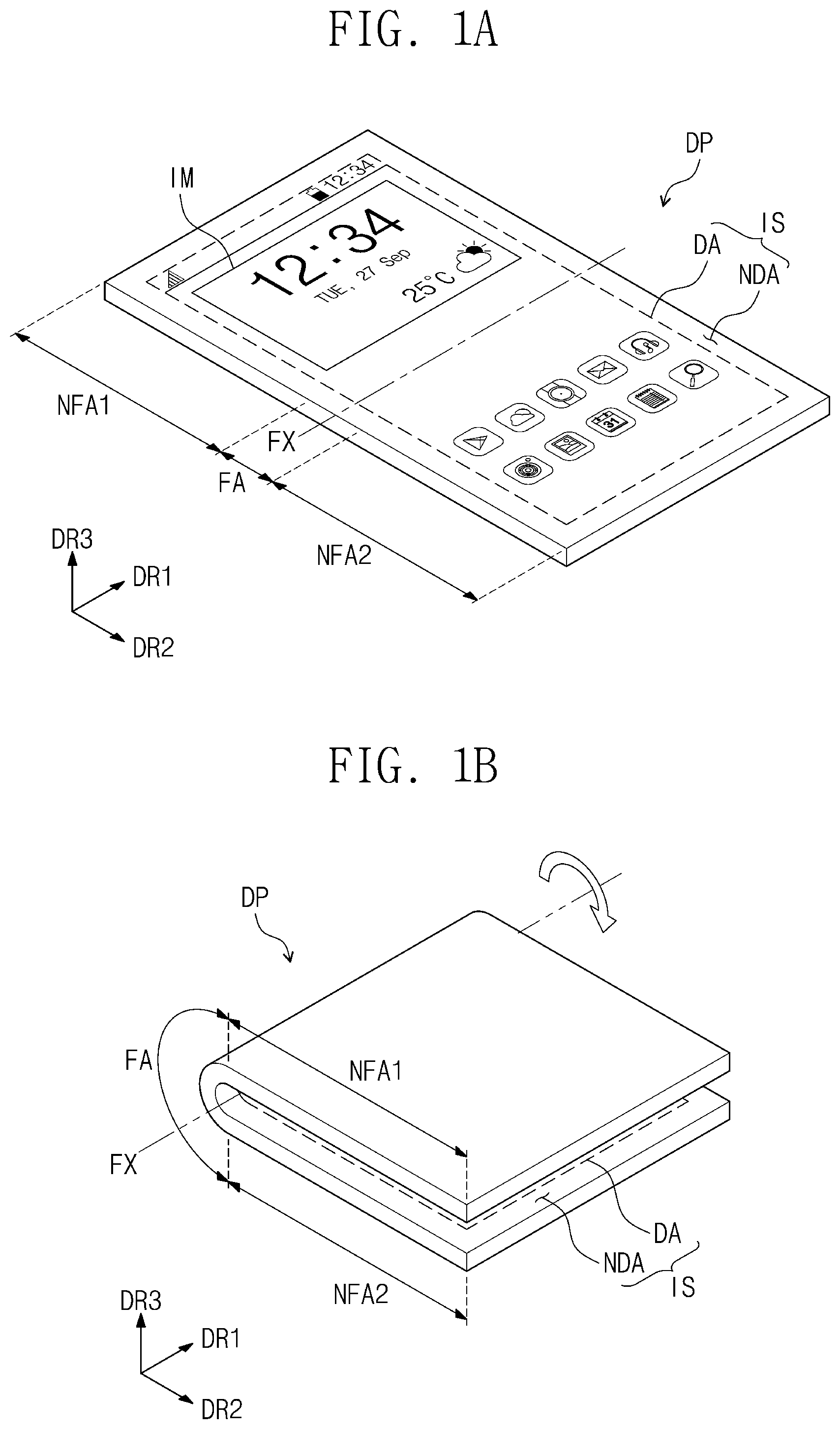
A is a perspective view showing a display panel DP according to an embodiment of the present inventive concepts. B is a perspective view showing the display panel DP shown in A in a folded state. C is a cross-sectional view showing the display panel DP shown in B in the folded state.
The display panel DP according to an embodiment of the present inventive concepts may be a device that is activated in response to electrical signals to display an image. In an embodiment, the display panel DP may be applied to various electronic devices, such as a mobile phone, a notebook computer, a tablet computer, a navigation unit, a game unit, or a television set. However, embodiments of the present inventive concepts are not limited thereto and the display panel DP may be applied to other small, medium and large sized electronic devices.
Referring to the embodiment A , the display panel DP may have a rectangular shape with relatively shorter sides in a first direction DR 1 and relatively longer sides in a second direction DR 2 crossing the first direction DR 1 . An upper surface of the display panel DP may be defined as a display surface IS. The display surface IS may extend in a plane defined by the first direction DR 1 and the second direction DR 2 . However, embodiments of the present inventive concepts are not limited thereto and the shape of the display panel DP may have a variety of shapes and the display surface IS may extend on one or more planes extending in a variety of different directions.
The display surface IS may include a display area DA and a non-display area NDA adjacent to the display area DA. The display area DA may be an area in which an image IM is displayed, and the non-display area NDA may be an area in which the image IM is not displayed. In an embodiment, the image IM may be at least one moving and/or still images. In the embodiment of A , the image IM is software application icons and a clock, temperature and calendar window. However embodiments of the present inventive concepts are not limited thereto and the image IM may be various different subject matter.
As shown in the embodiment of A , the display area DA may have a rectangular shape. The non-display area NDA may surround the display area DA. For example, as shown in the embodiment of A , the non-display area NDA may completely surround the display area DA (e.g., in the first and second directions DR 1 , DR 2 ). However, embodiments of the present inventive concepts are not limited thereto. For example, the shape of the display area DA and the shape of the non-display area NDA may have various different shapes. Additionally, the non-display area NDA may not surround one or more sides of the display area DA. For example, the non-display area NDA may be adjacent to only one side of the display area DA or may be omitted.
Meanwhile, upper (or front) and lower (or rear) surfaces of each member are defined with respect to a direction in which the image IM is displayed. The front and rear surfaces are opposite to each other in a third direction DR 3 , and a normal line direction of each of the font and lower surfaces may be substantially parallel to the third direction DR 3 .
Directions indicated by the first, second, and third directions DR 1 , DR 2 , and DR 3 may be relative to each other and may be changed to other directions. Hereinafter, the first, second, and third directions respectively are assigned with the same reference numerals as those of the first, second, and third directions DR 1 , DR 2 , and DR 3 .
The display panel DP of the present inventive concepts may be flexible. For example, the display panel DP may have a flexible property, and the display panel DP may be fully bent or may be bent in the scale of a few nanometers. For example, the display panel DP may be a curved display panel or a foldable display panel. However, embodiments of the present inventive concepts are not limited thereto. For example, in an embodiment, the display panel DP may be rigid.
As shown in the embodiments of A to 1 C , the display panel DP according to an embodiment may be folded or unfolded about a folding axis FX extending in one direction. The display panel DP may be inwardly folded (in-folding) or outwardly folded (out-folding) about the folding axis FX. The embodiment of A shows the unfolded display panel DP, and the embodiments of B and 1 C show the inwardly folded (in-folding) display panel DP.
In an embodiment, the folding axis FX may extend along one direction of the display panel DP. For example, the folding axis FX may correspond to an axis substantially parallel to the relatively shorter sides of the display panel DP (e.g. the first direction DR 1 ) as shown in the embodiments of A to 1 C . However, embodiments of the present inventive concepts are not limited thereto or thereby, and the folding axis may correspond to an axis substantially parallel to the relatively longer sides of the display panel DP (e.g., the second direction DR 2 ), may extend along a diagonal line between the first and the second directions DR 1 , DR 2 , etc.
The display panel DP may include a folding area FA in which a change in shape occurs with respect to the folding axis FX and first and second non-folding areas NFA 1 and NFA 2 respectively adjacent to both ends of the folding area FA such that the folding area FA is disposed between the first and second non-folding areas NFA 1 and NFA 2 . Referring to the embodiment of A , the display panel DP may include a first non-folding area NFA 1 adjacent to one side of die folding area FA (e.g., in the second direction DR 2 ), which is substantially parallel to the folding axis FX, and a second non-folding area NFA 2 adjacent to the other side of the folding area FA (e.g., in the second direction DR 2 ), which is substantially parallel to the folding axis FX. The embodiments of A to 1 C show one folding area FA. However, embodiments of the present inventive concepts are not limited thereto and the display panel DP may include a plurality of folding areas defined therein.
Referring to the embodiment of B , the display panel DP may be inwardly folded (in-folding) about the folding axis FX. When the display panel DP is inwardly folded (in-folding), the display surface IS of the first non-folding area NFA 1 and the display surface IS of the second non-folding area NFA 2 face each other. Accordingly, a rear surface of the display panel DP, which is opposite to the display surface IS of the display panel DP, may be exposed to the outside, and the display surface IS of the display panel DP may be protected from external impacts.
Meanwhile, the display panel DP may be outwardly folded (out-folding) about the folding axis FA. When the display panel DP is outwardly folded, the display surface IS of the first non-folding area NFA 1 , the second non-folding area NFA 2 , and the folding area FA may be exposed to the outside. The image IM may be displayed through the display surface IS exposed to the outside of the display panel DP that is outwardly folded.
Referring to the embodiment of , the display panel DP may include a display module DM and an encapsulation layer TFE. The encapsulation layer TFE may be disposed on the display module DM. The encapsulation layer TFE may cover the display module DM.
C shows a cross-section of the inwardly folded display panel DP, and an upper surface of the display module DM and the encapsulation layer TFE may face each other in the third direction DR 3 . The folded display panel DP may have a predetermined radius of curvature RR with respect to the folding axis FX. A stress applied to the folding area FA may vary depending on a value of the radius of curvature RR, and a delamination defect may occur between interfaces of each component of the display panel DP due to the stress.
According to the display panel DP of the present inventive concepts, the delamination defect between the display module DM and the encapsulation layer TFE covering the display module DM may be reduced or prevented. Accordingly, although the folding and unfolding operations are repeatedly performed, the display module DM and the encapsulation layer TFE are not easily separated from each other, and a reliability of the display panel DP may be increased. The display module DM and the encapsulation layer TFE will be described in detail later.
is a cross-sectional view showing the display panel DP according to an embodiment of the present inventive concepts. In an embodiment, the display panel DP may be a light emitting type display panel. For example, the display panel DP may be a liquid crystal display panel, an organic electroluminescence display panel, or a quantum dot light emitting display panel. However, embodiments of the present inventive concepts are not limited thereto. Hereinafter, for convenience of explanation, the display panel DP will be described as an organic electroluminescence display panel.
As shown in the embodiment of , the display panel DP may include a base layer BL, a circuit layer DP-CL, a light emitting element layer DP-LE, and the encapsulation layer TFE, which are sequentially stacked in the third direction DR 3 . The display panel DP may include a plurality of light emitting areas PXA that emit a light and a peripheral area NPXA surrounding the light emitting areas PXA.
In an embodiment, the base layer BL may be a flexible substrate and may be folded and unfolded. In an embodiment, the base layer BL may include a synthetic resin substrate. The synthetic resin substrate may include at least one material selected from a polyimide-based resin, an acrylic-based resin, a methacrylic-based resin, a polyisoprene-based resin, a vinyl-based resin, an epoxy-based resin, a urethane-based resin, a cellulose-based resin, a siloxane-based resin, a polyamide-based resin, and a perylene-based resin. However, embodiments of the present inventive concepts are not limited thereto or thereby. In an embodiment, the base layer BL may include a glass substrate, a metal substrate, or an organic/inorganic composite material, and the base layer BL may be rigid.
The circuit layer DP-CL may be disposed on the base layer BL (e.g., directly thereon in the third direction DR 3 ). In an embodiment, the circuit layer DP-CSL may include at least one insulating layer and a circuit element. The circuit element may include a signal line and a pixel driving circuit. In an embodiment, the circuit layer DP-CL may be formed by a coating or depositing process to form at insulating layer, a semiconductor layer, and a conductive layer and several photolithography processes to pattern the insulating layer, the semiconductor layer, and the conductive layer. However, embodiments of the present inventive concepts are not limited thereto.
As shown in the embodiment of , the circuit layer DP-CL may include a buffer layer BFL, a plurality of insulating layers, such as first to third insulating layers 10 , 20 , and 30 , and a plurality of transistors TR. The embodiment of shows two transistors TR. However, embodiments of the present inventive concepts are not limited thereto and the number of the transistors TR may vary.
The buffer layer BFL may be disposed on the base layer BL (e.g., directly thereon in the third direction DR 3 ). The buffer layer BFL may be formed on an upper surface of the base layer BL. The buffer BFL layer may include at least one inorganic layer. Its an embodiment, the inorganic layer may include at least one compound selected from aluminum oxide, titanium oxide, silicon oxide, silicon oxynitride, zirconium oxide, and hafnium oxide. The buffer layer BFL may have a multi-layer structure in which a silicon oxide layer and a silicon nitride layer are alternately stacked one on another. However, embodiments of the present inventive concepts are not limited thereto and the material for the buffer layer BFL may vary.
A semiconductor pattern may be disposed on the buffer layer BFL (e.g., directly thereon in the third direction DR 3 ). The buffer layer BFL may increase an adhesion between the base layer BL and the semiconductor pattern. In an embodiment, the semiconductor pattern may include polysilicon, amorphous silicon or metal oxide. However, embodiments of the present inventive concepts are not limited thereto.
shows an arrangement of an active AD, a source SD, a drain DD, and a gate GD that form the transistor TR. The active AD, the source SD, and the drain DD may be distinct from each other by a doping concentration or a conductivity of the semiconductor pattern.
A first insulating layer 10 may be disposed on the buffer layer BFL (e.g., directly thereon in the third direction DR 3 ). The first insulating layer 10 may cover the semiconductor pattern. In an embodiment, the first insulating layer 10 may be an inorganic layer and/or an organic layer and may have a single-layer or multi-layer structure.
The gate GD may be disposed on the first insulating layer 10 (e.g., directly thereon in the third direction DR 3 ). In an embodiment, the gate GD may be a portion of a metal pattern. The gate GD may overlap the active AD (e.g., in the third direction DR 3 ).
A second insulating layer 20 may be disposed on the first insulating layer 10 (e.g., directly thereon in the third direction DR 3 ) and may cover the gate GD. In an embodiment, the second insulating layer 20 may be an inorganic layer and/or an organic layer and may have a single-layer or multi-layer structure.
A third insulating layer 30 may be disposed on the second insulating layer 20 (e.g., directly thereon in the third direction DR 3 ). In an embodiment, the third insulating layer 30 may be an inorganic layer and/or an organic layer and may have a single-layer structure of a silicon oxide layer.
In an embodiment, each of the first insulating layer 10 , the second insulating layer 20 , and the third insulating layer 30 may include at least one compound selected from aluminum oxide, titanium oxide, silicon oxide, silicon oxynitride, zirconium oxide, and hafnium oxide. However, embodiments of the present inventive concepts are not limited thereto and the materials for the first insulating layer 10 , the second insulating layer 20 , and the third insulating layer 30 may vary.
The light emitting element layer DP-LE may be disposed on the circuit layer DP-CL (e.g., directly thereon in the third direction DR 3 ). The light emitting element layer DP-LE may include a light emitting element LE and a pixel definition layer PDL. The pixel definition layer PDL may be include an opening OP defined therethrough, and the light emitting element LE may be disposed to overlap the opening OP. The light emitting element LE may be disposed in the opening OP.
The light emitting element LE may include a first electrode AE, a second electrode CE, and a light emitting layer EML disposed between the first and second electrodes AE and CE (e.g., in the third direction DR 3 ). The light emitting element LE may further include functional layers disposed between the light emitting layer EML and each of the first electrode AE and the second electrode CE. For example, in the embodiment of , the light emitting element LE may include the first electrode AE, the second electrode CE, the light emitting layer EML, a hole control layer HCL, and an electron control layer ECL. However, embodiments of the present inventive concepts are not limited thereto and the functional layers included in the light emitting element LE may vary.
The first electrode AE may be disposed on the third insulating layer 30 (e.g., directly is thereon in the third direction DR 3 ). The first electrode AE may be connected directly or indirectly to the transistor TR. At least a partial portion of the first electrode AE may be exposed through the opening OP defined through the pixel definition layer PDL. For example, as shown in the embodiment of , a central portion of the first electrode AE (e.g., in the first direction DR 1 ) may be exposed by the opening OP.
The light emitting layer EML may be disposed between the first electrode AE and the second electrode CE (e.g., in the third direction DR 3 ). In an embodiment, the light emitting layer EML may be activated according to a difference in electric potential between the first electrode AE and the second electrode CE and may generate a light. The light generated by the light emitting layer EML may exit through the upper surface of the display panel DP. For example, the generated light may be a blue light. However, embodiments of the present inventive concepts are not limited thereto.
As shown in the embodiment of , the light emitting element LE may include the hole control layer HCL disposed between the first electrode AE and the light emitting layer EML (e.g., in the third direction DR 3 ) and the electron control layer ECL disposed between the second electrode CE and the light emitting layer EML (e.g., in the third direction DR 3 ). The hole control layer HCL may include at least one of a hole transport layer and a hole injection layer. The electron control layer ECL may include at least one of an electron transport layer and an electron injection layer.
The pixel definition layer PDL may be disposed on the circuit layer DP-CL. The pixel definition layer PDL may be disposed on the third, insulating layer 30 included its the circuit layer DP-CL. For example, as shown in the embodiment of , a lower portion of the pixel definition layer PDL may directly contact an upper surface of third insulation layer 30 and lateral ends of the first electrode AE. In an embodiment, the opening OP defined through the pixel definition layer PDL may be provided in plural, and the openings OP may respectively overlap the light emitting areas PXA (e.g., in the third direction DR 3 ). The pixel definition layer PDL may be disposed to overlap the peripheral area NPXA (e.g., in the third direction DR 3 ). In an embodiment, the pixel definition layer PDL may include an organic layer.
The pixel definition layer PDL may include a base portion BS and a plurality of barrier portions, such as first and second barrier portions BK 1 and BK 2 . A lower surface of first and second barrier portions BK 1 and BK 2 may be in direct contact with the base portion BS. The first and second barrier portions BK 1 and BK 2 may be spaced apart from each other (e.g., in the first direction DR 1 ) to form a space. However, embodiments of the present inventive concepts are not limited thereto and the configuration of the pixel definition layer PDL may vary. For example, in an embodiment the base portion BS included in the pixel definition layer PDL may be omitted.
The light emitting later EML may be commonly disposed or may be independently disposed in the light emitting areas PXA. The expression “independently disposed” means that the light emitting layer EML is divided into discrete, plural portions and the portions are respectively disposed in the light emitting areas PXA to be separated from each other as shown in the embodiment of . The expression “commonly disposed” means that the light emitting layer EML is disposed commonly in the light emitting areas PXA and the peripheral area NPXA and is not disposed separately.
As shown in the embodiment of , the hole control layer HCL, the electron control layer ECL, and the second electrode CE be commonly disposed in the light emitting areas PXA and the peripheral area NPXA. The hole control layer HCL, the electron control layer ECL, and the second electrode CE, which are commonly disposed, may be defined as a common layer EL. The common layer EL may be disposed on the pixel definition layer PDL, and the common layer EL may be formed to correspond to an uneven upper surface of the pixel definition layer PDL. For example, as shown in the embodiment of , the hole control layer HCL, the electron control layer ECL, and the second electrode CE may correspond to a shape of the uneven upper surface of the pixel definition layer PDL. However, embodiments of the present inventive concepts are not limited thereto and the elements of the comm on layer EL may vary.
The encapsulation layer TFE may be disposed on the light emitting element layer DP-LE (e.g., directly thereon in the third direction DR 3 ). The encapsulation layer TFE may encapsulate the light emitting element layer DP-LE. The encapsulation layer TFE may include at least one insulating layer. In an embodiment, the encapsulation layer TFE may include at least one organic layer and at least one inorganic layer. For example, as shown in the embodiment of , the encapsulation layer TFE may include a first inorganic layer IO 1 , an organic layer MN, and a second inorganic layer IO 2 sequentially stacked on the light emitting element layer DP-LE in the third direction DR 3 .
The first inorganic layer IO 1 and the second inorganic layer IO 2 may protect the light emitting element layer DP-LE from oxygen and moisture, and the organic layer MN may protect the light emitting element layer DP-LE from foreign substance such as dust particles. For example, in an embodiment, the first inorganic layer IO 1 and the second inorganic layer IO 2 may include a silicon nitride layer, a silicon oxynitride layer, a silicon oxide layer, a titanium oxide layer, or an aluminum oxide layer. However, embodiments of the present inventive concepts are not limited thereto. In an embodiment, the organic layer MN may include an acrylic-based organic layer. However, embodiments of the present inventive concepts are not limited thereto.
The first inorganic layer IO 1 may be disposed on the common layer EL. For example, a lower surface of the first inorganic layer IO 1 may be in direct contact with the common layer EL. As shown in the embodiment of , the first inorganic layer IO 1 may be n direct contact with the second electrode CE that is commonly disposed. The organic layer MN may be disposed on the first inorganic layer IO 1 . For example, the organic layer MN may be directly disposed on the first inorganic layer IO 1 and an upper surface of the first inorganic layer IO 1 may be in direct contact with the organic layer MN.
In comparative embodiments, when a display panel is folded, a light emitting element layer and an encapsulation layer, or an inorganic layer and an organic layer of the encapsulation layer may be separated from each other due to the stress applied to a folding area (refer to C ). However, the display panel DP of the present inventive concepts may reduce or prevent the delamination defect between the light emitting element layer DP-LE and the encapsulation layer TFE, and between the first inorganic layer IO 1 and the organic layer MN of the encapsulation layer TFE.
The level of the upper surface of the pixel definition layer PDL (e.g., distance in the third direction DR 3 from an upper surface of the base layer BL) may be uneven by the first and second barrier portions BK 1 and BK 2 and the predetermined space defined by the first and second barrier portions BK 1 and BK 2 . The first inorganic layer IO 1 may include a curved upper surface corresponding to a shape of the curved upper surface of the pixel definition layer PDL. The first inorganic layer IO 1 may be deposited in various shapes by covering the first and second barrier portions BK 1 and BK 2 of the pixel definition layer PDL, and thus, the delamination defect between the light emitting element layer DR-LE and the encapsulation layer TFE and the delamination defect between the stacked components in the encapsulation layer TFE may be reduced or prevented.
is a plan view showing a display panel according to an embodiment of the present inventive concepts. For the convenience of explanation, shows a plan view of the pixel definition layer PDL, and portions corresponding to first to fourth barrier portions BK 1 , BK 2 , BK 3 and BK 4 are shaded in the illustration. The common layer EL, the first inorganic layer IO 1 and the organic layer MN are disposed on the pixel definition layer PDL shown in the embodiment of .
The light emitting areas PXA may be divided into a plurality of groups according to a color of a light exiting from the display panel DP. For example, as shown in the embodiment of , the display panel DP may include three light emitting areas, such as the first to third light emitting areas PXA 1 , PXA 2 , and PXA 3 , respectively emitting a blue light, a red light, and a green light. However, embodiments of the present inventive concepts are not limited thereto and the number of the light emitting areas and the colors that the light emitting areas may emit may vary. In an embodiment, the light emitting areas may include a first light emitting area PXA 1 emitting the blue light, a second light emitting area PXA 2 emitting the red light, and a third light emitting area PXA 3 emitting the green light.
The first to third light emitting areas PXA 1 , PXA 2 , and PXA 3 may be spaced apart from each other in a plane (e.g., a plane defined in the first and second directions DR 1 , DR 2 ). The first to third light emitting areas PXA 1 , PXA 2 , and PXA 3 may be separated from each other by the pixel definition layer PDL. The peripheral area NPXA may be an area between the first to third light emitting areas PXA 1 , PXA 2 , and PXA 3 adjacent to each other and may correspond to the pixel definition layer PDL. The peripheral area NPXA may serve as a boundary between the first to third light emitting areas PXA 1 , PXA 2 , and PXA 3 and may prevent colors of lights respectively exiting from the first to third light emitting areas PXA 1 , PXA 2 , and PXA 3 from being mixed with each other.
As shown in the embodiment of , the first to third light emitting areas PXA 1 , PXA 2 , and PXA 3 may have different sizes from each other depending on a wavelength range of the light exiting therefrom. The size of the first to third light emitting areas PXA 1 , PXA 2 , and PXA 3 may indicate an area in a plane defined in the first direction DR 1 and the second direction DR 2 . However, embodiments of the present inventive concepts should not be limited thereto or thereby, and the sizes of two or more of the first to third light emitting areas PXA 1 , PXA 2 , and PXA 3 may be substantially similar to each other.
In an embodiment, the first to third light emitting areas PXA 1 , PXA 2 , and PXA 3 may be arranged in a pentile pattern. Referring to the embodiment of , the first light emitting area PXA 1 and the second light emitting area PXA 2 may be alternately arranged with each other in the first direction DR 1 and the second direction DR 2 , and the third light emitting area PXA 3 may be substantially disposed in an area between the first light emitting areas PXA 1 and the second light emitting areas PXA 2 along a diagonal direction (e.g., a direction between the first and second directions DR 1 , DR 2 and perpendicular to the third direction DR 3 ). However, embodiments of the present inventive concepts are not limited thereto and the arrangement of the first to third light emitting areas PXA 1 , PXA 2 , and PXA 3 may vary. For example, in an embodiment, the first to third light emitting areas PXA 1 , PXA 2 , and PXA 3 may be arranged in a stripe pattern or a lozenge pattern.
The pixel definition layer PDL may be provided with a plurality of openings, such as first to third openings OP 1 , OP 2 , and OP 3 . The first to third openings OP 1 , OP 2 , and OP 3 may correspond to the shape of the first to third light emitting areas PXA 1 , PXA 2 , and PXA 3 in a plane (e.g., in a plane defined in the first and second directions DR 1 , DR 2 ). The pixel definition layer PDL shown in the embodiment of may be provided with a first opening OP 1 corresponding to the shape of the first light emitting area PXA 1 , a second opening OP 2 corresponding to the shape of the second light emitting area PXA 2 , and a third opening OP 3 corresponding to the shape of the third light emitting area PXA 3 . However, the shapes of the first to third openings OP 1 , OP 2 , OP 3 should not be limited to those shown in the embodiment of , and the shapes of the first to third openings OP 1 , OP 2 , OP 3 may vary, such as depending on the shapes of the light emitting areas.
The pixel definition layer PDL may include a plurality of barrier portions. Some barrier portions of the of the barrier portions may be disposed adjacent to each other. The embodiment of shows first, second, third, and fourth barrier portions BK 1 , BK 2 , BK 3 , and BK 4 disposed adjacent to each other (e.g., in the first and/or second directions DR 1 , DR 2 ). However, the number of the barrier portions disposed adjacent to each other should not be limited thereto provided that the pixel definition layer PDL includes the barrier portions defining the predetermined space while being spaced apart from each other.
As shown in the embodiment of , the pixel definition layer PDL may include the first barrier portion BK 1 and the second barrier portion BK 2 , which are spaced apart from each other by a predetermined distance in the first direction DR 1 to form the space. The pixel definition layer PDL may further include the third barrier portion BK 3 that is spaced apart from the first barrier portion BK 1 by a predetermined distance in the second direction DR 2 to form the space.
In the space defined by the barrier portions, the distance between the barrier portions may vary depending on a location thereof. For example, a distance in the first direction DR 1 between the first barrier portion BK 1 and the second barrier portion BK 2 may be different from a distance in the second direction DR 2 between the first barrier portion BK 1 and the third barrier portion BK 3
The first inorganic layer IO 1 (refer to A ) ma be disposed on the pixel definition layer PDL and may include an uneven upper surface corresponding to the space defined by the barrier portions. Accordingly, a groove GM may be defined by the upper surface of the first inorganic layer IO 1 to overlap the space. The groove GM may have a shape corresponding to a shape of the space defined by the barrier portions when viewed in a plane.
The plurality of the barrier portions disposed adjacent to each other may be defined as one barrier group BKG. For example, the embodiment of includes the barrier group BKG defined by the first, second, third, and fourth barrier portions BK 1 , BK 2 , BK 3 , and BK 4 disposed adjacent to each other. However, embodiments of the present inventive concepts are not limited thereto and the barrier group BKG may vary such as shown in the embodiments of A to 8 C .
A shape obtained by connecting an outer side of the barrier portions disposed adjacent to each other and the space defined by the barrier portions in a plane may vary. For example, in an embodiment, the shape may be a polygonal shape, such as a triangular shape, a quadrangular shape, a lozenge shape, and the like, or a circular shape. shows the shape obtained by connecting the outer side of the barrier portions and the space defined by the barrier portions with a dotted line, and the shape may be defined as a shape of the barrier group BKG. The embodiment of shows the shape of the barrier group BKG having a quadrangular shape. However, embodiments of the present inventive concepts are not limited thereto and the shape may vary as long as the shape is obtained by connecting the outer side of the harder portions defining the space.
In an embodiment, the barrier group BKG may be provided in plural, and the plurality of the barrier groups BKG may be disposed in a portion of the peripheral area NPXA to overlap the peripheral area NPXA. The barrier group BKG may be disposed not to overlap the first to third light emitting areas PXA 1 , PXA 2 , and PXA 3 (e.g., in third direction DR 3 ). As the number of the barrier groups BKG disposed on the light emitting element layer DP-LE (refer to ) increases, a resistance of the display panel DP to external tensile force may be strengthened. In addition, the delamination defect between the common layer EL and the pixel definition layer PDL and between the common layer EL and the first inorganic layer IO 1 , which is caused by the folding operation, may be more effectively reduced or prevented.
A is a cross-sectional view taken along line I-I′ of to show the pixel definition layer PDL and the encapsulation layer TFE. B is a cross-sectional view showing a pixel definition layer PDL and an encapsulation layer TFE, which have substantially the same configurations as those of A except a shape of a first inorganic layer IO 1 in a side view.
Referring to the embodiment of A , the first barrier portion BK 1 and the second barrier portion BK 2 , which are included in the pixel definition layer PDL, may form a first space SP 1 having a first distance D 1 (refer to ) in the first direction DR 1 (or a first length D 1 in the first direction DR 1 ). A first groove GM 1 may be defined by the upper surface of the first int inorganic layer IO 1 overlapping the first space SP 1 . The first inorganic layer IO 1 overlapping the first space SP 1 may have a thickness that varies depending on its position.
In an embodiment, the first inorganic layer IO 1 may be formed on the light emitting element layer DP-LE by a chemical vapor deposition (CVD) process. The thickness of the first inorganic layer IO 1 may vary due to a material of a composition forming the first inorganic layer IO 1 , a deposition angle, and a shape of an upper surface on which the first inorganic layer IO 1 is deposited. The deposition shape of the first inorganic layer IO 1 may be controlled by, adjusting the thickness of the first inorganic layer IO 3 during the deposition process.
As shown in the embodiment of A , the first inorganic layer IO 1 overlapping the first space SP 1 may include first, second, and third portions IO 1 - 1 , IO 1 - 2 , and IO 1 - 3 . The first, second, and third portions IO 1 - 1 , IO 1 - 2 , and IO 1 - 3 may be formed to correspond to the shape of the first space SP 1 .
As shown in the embodiment of A , the first portion IO 1 - 1 of the first inorganic layer IO 1 may be disposed to be substantially parallel to the light emitting element layer DP-LE. A normal line direction of an upper surface of the first portion IO 1 - 1 may be substantially parallel to the third direction DR 3 . Each of the second portion IO 1 - 2 and the third portion IO 1 - 3 of the first inorganic layer IO 1 may be bent from the first portion IO 1 - 1 . The second portion IO 1 - 2 and the third portion IO 1 - 3 may be spaced apart from each other in the first direction DR 1 and may face each other.
As shown in the embodiment of A , the first groove GM 1 may be defined by the upper surfaces of the first, second, and third portions IO 1 - 1 , IO 1 - 2 , and IO 1 - 3 . The first groove GM 1 may be defined by being recessed from a plane. The organic layer MN may be filled in the recessed first groove GM 1 . As the organic layer MN is filled in the first groove GM 1 , the delamination reelect between the organic layer MN and the first inorganic layer IO 1 , which is caused by the folding operation, may be reduced or prevented.
A thickness (e.g., length in the first direction DR 1 ) of the second portion IO 1 - 2 and a thickness (e.g., length in the first direction DR 1 ) of the third portion IO 1 - 3 may vary depending on its position. For example, as shown in the embodiment of A , upper portions of the second portion IO 1 - 2 and the third portion IO 1 - 3 may be relatively thriller away from the first portion IO 1 - 1 in the third direction DR 3 , and lower portions of the second portion IO 1 - 2 and the third portion IO 1 - 3 may be relatively closer to the first portion IO 1 - 1 in the third direction DR 3 . The thickness of the upper portion of each of the second portion IO 1 - 2 and the third portion IO 1 - 3 may be greater than the thickness of the lower portion of each of the second portion IO 1 - 2 and the third portion IO 1 - 3 .
As shown in the embodiment of A , the thickness t 1 of the upper portion of the second portion IO 1 - 2 may be greater than the thickness t 2 of the lower portion of the second portion IO 1 - 2 . The shape of the first inorganic layer IO 1 deposited on the pixel definition layer PDL and the common layer EL may be changed due to the different thicknesses of the upper portion and the lower portion. For example, the upper portion of the second portion IO 1 - 2 may protrude in the first direction DR 1 and may have an overhang shape that is due to the greater thickness of the upper portion of the second portion IO 1 - 2 as compared to the lower portion of the second portion IO 1 - 2 .
As shown in the embodiment of A , the thickness of the second portion IO 1 - 2 may gradually increase and the inner wall which defines a portion of the first groove GM 1 may be oblique with respect to the base portion BS in a direction towards the third portion IO 1 - 3 . The upper portion of the second portion IO 1 - 2 may protrude from an adjacent portion of the second portion IO 1 - 2 in a non-gradual manner and may form the overhang-shaped portion. The thickness of the third portion IO 1 - 3 may have a similar arrangement and the inner wall of the third portion IO 1 - 3 may be oblique with respect to the base portion BS in a direction towards the second portion IO 1 - 2 .
The first groove GM 1 may have a width (e.g., length in the first direction DR 1 ) that changes depending on its position. The shape of the first groove GM 1 defined by the upper surfaces of the first, second, and third portions IO 1 - 1 , IO 1 - 2 , and IO 1 - 3 may vary due to the thickness of the first, second, and third portions IO 1 - 1 , IO 1 - 2 , and IO 1 - 3 . For example, an upper portion of the first groove GM 1 may have a width t 3 that is smaller than a width t 4 of a lower portion of the first groove GM 1 .
Due to the first inorganic layer IO 1 having the overhang shape in some areas, the width t 3 of the upper portion of the first groove GM 1 may be relatively narrower than the width t 4 of the lower portion of the first groove GM 1 .
The organic layer MN may be in direct contact with the upper surface of the first inorganic layer IO 1 . In an embodiment, the organic layer MN may be formed by coating a composition forming the organic layer MN on the upper surface of the first inorganic layer IO 1 and curing the composition. During the forming of the organic layer MN, the composition for the organic layer MN may be filled in the first groove GM 1 and may be cured. The adhesion between the organic layer MN and the first inorganic layer IO 1 may become stronger by a force of an interface between the organic layer MN filled in the first groove GM 1 and the first inorganic layer IO 1 and the shape of the first groove GM 1 of which the width of the upper portion is relatively narrow as compared to the width of the lower portion thereof. Accordingly, the delamination defect between the organic layer MN and the first inorganic layer IO 1 , which is caused by the folding operation, may be reduced or prevented.
As shown in the embodiment of A , the first inorganic layer IO 1 may be disposed in direct contact with an upper surface of the common layer EL. The first inorganic layer IO 1 and the common layer EL, which are disposed to overlap the first space SP 1 , may be in direct contact with each other along the first direction DR 1 that is a lateral direction, and thus, the first inorganic layer IO 1 may apply a pressure (e.g., a pressure in the third direction DR 3 towards the base portion BS) to allow the common layer EL to be fully attached to the pixel definition layer PDL. Accordingly, the delamination defect between the first inorganic layer IO 1 and the common layer EL and between the common layer EL and the pixel definition layer PDL, which is caused by the folding operation, may be reduced or prevented.
The first inorganic layer IO 1 shown in the embodiment of B has substantially the same configuration as the first inorganic layer IO 1 shown in the embodiment of A except the shape of the first inorganic layer IO 1 and the shape of the first groove GM 1 , which are disposed to overlap the first space SP 1 .
The thickness t 1 (e.g., length in the first direction DR 1 ) of the upper portion of the second portion IO 1 - 2 of the first inorganic layer IO 1 may be greater than the thickness t 2 of the lower portion of the second portion IO 1 - 2 . However, different from the shape of A , the second portion IO 1 - 2 and the third portion IO 1 - 3 may have a shape in which the thickness of each of the second portion IO 1 - 2 and the third portion IO 1 - 3 gradually increase as a distance from the first portion IO 1 - 1 increases along the third direction DR 3 and the upper portions of the second and third portions IO 1 - 2 , IO 1 - 3 may not protrude to form the overhang shape. Accordingly, a width t 3 (e.g., length in the first direction DR 1 ) of the upper portion of the first groove GM 1 shown in B may be greater than the width t 3 of the upper portion of the first groove GM 1 shown in A .
As the width t 3 of the upper portion of the first groove GM 1 decreases, the organic layer MN filled in the first groove GM 1 may not easily come out from the first groove GM 1 , and thus, the organic layer MN and the first inorganic layer IO 1 may not be easily separated from each other in a delamination defect. The width and the shape of the first groove GM 1 may be comforted by adjusting the arrangement distance between the first and second barrier portions BK 1 and BK 2 and the deposition process of the first inorganic layer IO 1 . Therefore, the organic layer MN array be sufficiently filled in the first groove GM 1 and the delamination defect of the organic layer MN may be effectively reduced or prevented by controlling the width and the shape of the first groove GM 1 .
A and 5 B are cross-sectional views showing a pixel definition layer, a common layer, and a first inorganic layer according to an embodiment of the present inventive concepts. The pixel definition layer PDL, the common layer EL, and the first inorganic layer IO 1 include substantially the same configurations as those shown in the embodiments of to 4 B , and thus, a description of substantially similar elements described with reference to to 4 B may be applied to the pixel definition layer PDL, the common layer EL, and the first inorganic layer IO 1 of the embodiments of A and 5 B and may not be repeated for convenience of explanation. Referring to the embodiments of A and 5 B , a shape of a first barrier portion BK 1 and a shape of a second barrier portion BK 2 , which are included in the pixel definition layer PDL, will be mainly described.
Referring to the embodiments of A and 5 B , the first barrier portion BK 1 may include a lower surface B 1 -B and a first lateral surface B 1 -S. The second barrier portion BK 2 may include a lower surface B 2 -B and a second lateral surface B 2 -S. Each of the lower surface B 1 -B of the first harder portion BK 1 and the lower surface B 2 -B of the second barrier portion BK 2 may be substantially parallel to a plane defined b the first direction DR 1 and the second direction DR 2 . The lower surfaces B 1 -B, B 2 -B of the first and second barrier portions BK 1 , BK 2 may be substantially parallel with an upper surface of the base portion BS. The first lateral surface B 1 -S and the second lateral surface B 2 -S may be spaced apart from each other in the first direction DR 1 and may face each other.
As shown in the embodiment of A , an angle between the lower surface B 1 -B and the first lateral surface B 1 -S of the first barrier portion BK 1 may be defined as a first angle θ 1 , and an angle between the lower surface B 2 -B and the second lateral surface B 2 -S of the second barrier portion BK 2 may be defined as a second angle θ 2 . In an embodiment, each of the first angle θ 1 and the second angle θ 2 may be in a range of about 45 degrees to about 180 degrees.
In the embodiment of A , the first barrier portion BK 1 and the second barrier portion BK 2 have a first angle θ 1 and second angle θ 2 , respectively, that are both greater than about 90 degrees. In the embodiment of B , the first barrier portion BK 1 and the second barrier portion BK 2 have the first angle θ 1 and the second angle θ 2 , respectively, that are both less than about 90 degrees. As shown in the embodiment of A , the first angle θ 1 and the second angle θ 2 may be about 90 degrees, and the first lateral surface B 1 -S and the second lateral surface B 2 -S may be substantially parallel to each other.
The first angle θ 1 and the second angle θ 2 may exert an influence on a frictional force between the common layer EL and the first inorganic layer IO 1 or a frictional force between the pixel definition layer PDL and the first inorganic layer IO 1 , which are disposed on the first lateral surface B 1 -S and the second lateral surface B 2 -S. As the first angle θ 1 and the second angle θ 2 increase, the frictional force at an interface between components increases, and as the frictional force increases, the components may be more difficult to be separated from each other. Accordingly, the delamination defect between the common layer EL and the first inorganic layer IO 1 , which are disposed on the first and second barrier portions BK 1 and BK 2 , may be reduced or prevented by adjusting the first angle θ 1 and the second angle θ 2 .
is a cross-sectional view taken along line II-II′ of to show a pixel definition layer and at encapsulation layer. The pixel definition layer PDL may include first, second, and third barrier portions BK 1 , BK 2 , and BK 3 . The first barrier portion BK 1 may be spaced apart from the second barrier portion BK 2 (e.g., in the first direction DR 1 ) and may define a first space SP 1 having a first distance D 1 in the first direction DR 1 (or a first length D 1 in the first direction DR 1 ). The third barrier portion BK 3 may be spaced apart from the first barrier portion BK 1 (e.g., in the second direction DR 2 ) and may define a second spaces SP 2 having a second distance D 2 in the second direction DR 2 (or a second length D 2 in the second direction DR 2 ).
A plurality of barrier portions, such as the first to third barrier portions BK 1 , BK 2 , and BK 3 , included in the pixel definition layer PDL and adjacent to each other may be spaced apart from each other at different distances. For example, as shown in the embodiment of , the first distance D 1 may be less than the second distance D 2 . A first inorganic layer IO 1 deposited to overlap the space having a relatively larger distance may be easily deposited at a relatively uniform thickness.
The adhesion between the pixel definition layer PDL, a common layer EL, and the first inorganic layer IO 1 may increase by the first inorganic layer IO 1 disposed to overlap the space defined by the barrier portions. Accordingly, the delamination defect between the pixel definition layer PDL, the common layer EL, and the first inorganic layer IO 1 may be reduced or prevented.
The deposition shape of the first inorganic layer IO 1 overlapping the spaces formed with different distances may be different from each other to correspond to the spaces. Thus, grooves defined by the upper surface of the first inorganic layer IO 1 overlapping the spaces formed with different distances may have different widths and different shapes.
A first groove GM 1 may be defined by the upper surface of the first inorganic layer IO 1 overlapping the first space SP 1 , and a second groove GM 2 may be defined by the upper surface of the first inorganic layer IO 1 overlapping the second space SP 2 . The first groove GM 1 and the second groove GM 2 may have different shapes from each other.
The first groove GM 1 may have a shape in which a width t 3 (e.g., length in the first direction DR 1 ) of an upper portion of the first groove GM 1 is less than a width t 4 (e.g. length in the first direction DR 1 ) of a lower portion of the first groove GM 1 . The second groove GM 2 may have a shape in which a width t 5 (e.g., length in the second direction DR 2 ) of an upper portion of the second groove GM 2 is equal to or similar to a width (e.g., length in the second direction DR 2 ) of a lower portion of the second groove GM 2 , or the width t 5 of the upper portion of the second groove GM 2 may be greater than the width of the lower portion of the second groove GM 2 .
An organic layer MN filled in the first groove GM 1 having the width t 3 of the upper portion that is relatively small does not easily come out from the first groove GM 1 , and thus, the first inorganic layer IO 1 and the organic layer MN may not be easily separated from each other. The organic layer MN filled in the second groove GM 2 whose width t 5 of the upper portion is relatively greater than the width t 3 of the upper portion of the first groove GM 1 may be sufficiently filled in the space defined as the second groove GM 2 without leaving an empty space.
In an embodiment, the first space SP 1 and the second space SP 2 may be a space formed integrally and may not be discrete and separated from each other. Accordingly, the first groove GM 1 and the second groove GM 2 defined by the upper surface of the first inorganic layer IO 1 may be defined integrally.
A and 7 B show a pixel definition layer and an encapsulation layer according to an embodiment of the present inventive concepts. Components include substantially the same configurations as those of the embodiments of to 4 B , and thus, the descriptions with reference to the embodiments to 4 B may be applied to the components of A and 7 B and a repeated description may not be provided for convenience of explanation. In the embodiments of A and 7 B the pixel definition layer PDL is different from that shown in the embodiment of A , and different features from the pixel definition layer PDL of the embodiment of A will be mainly described.
In the pixel definition layer PDL shown in the embodiment of A , the base portion BS may be omitted. A plurality of barrier portions, such as the first and second barrier portions BK 1 and BK 2 , included in the pixel definition layer PDL may be disposed to be in direct contact with an upper surface of the third insulating layer 30 .
A first barrier portion BK 1 and a second barrier portion BK 2 , which are spaced apart from each other to define a predetermined first space SP 1 , may directly contact the upper surface of the third insulating layer 30 included in the circuit layer DP-CL (refer to ). A lower surface of the common layer EL disposed to overlap the first space SP 1 may directly contact the upper surface of the third insulating layer 30 . Outer lateral sides of the first barrier portion BK 1 and the second barrier portion BK 2 may extend at an oblique angle with respect to the upper surface of the third insulating layer 30 .
The pixel definition layer PDL shown in the embodiment of B may include a base portion BS and a plurality of barrier portions, such as first and second barrier portions BK 1 and BK 2 , that are integrally formed with the base portion BS. For example, in an embodiment, the first and second barrier portions BK 1 and BK 2 of the pixel definition layer PDL may be formed by etching portions of a layer with a flat upper surface. The base portion BS and the first and second barrier portions BK 1 and BK 2 may include the same material. However, embodiments of the present inventive concepts are not limited thereto and the pixel definition layer PDL may vary. For example, the pixel definition layer may be formed by disposing the first and second barrier portions BK 1 and BK 2 on the base portion BS with the flat upper surface, and the base portion BS may include a material that is different from that of the first and second barrier portions BK 1 and BK 2 .
A to 8 C are plan views showing pixel definition layers according to embodiments of the present inventive concepts. A to 8 C show various shapes of a plurality of barrier portions in a plane according to various embodiments of the present inventive concepts. For convenience of explanation, the barrier portions are shaded in the illustration.
Each of the first to fourth barrier portions BK 1 , BK 2 , BK 3 , and BK 4 may be provided in plural and may have a pattern shape in a plane. Various examples of the first to fourth barrier portions BK 1 , BK 2 , BK 3 , and BK 4 having the pattern shape are shown in the embodiments of A to 8 C . However, embodiments of the present inventive concepts are not limited thereto and the pattern shape may vary provided the pattern is formed by the first to fourth barrier portions BK 1 , BK 2 , BK 3 , and BK 4 arranged in a certain rule.
As shown in the embodiment of A , predetermined first and second spaces SP 1 and SP 2 defined by the first to fourth barrier portions BK 1 , BK 2 , BK 3 , and BK 4 may be arranged in a radial shape with respect to an imaginary center CP when viewed in a plane. In the present specification, the term “radial shape” means a shape in which the spaces extend in several directions with respect to the imaginary center CP.
Referring to the embodiments of A and 8 B , a width D 3 of the first, space SP 1 may be different from a width D 4 of the second space SP 2 when viewed in a plane. The first and second spaces SP 1 and SP 2 having different widths may be integrally formed with each other.
As shown in the embodiment of B , the second space SP 2 may extend longitudinally substantially in the first direction DR 1 and the second direction DR 2 crossing the first direction DR 1 at the imaginary center CP. The first space SP 1 may extend in a diagonal direction between the first direction DR 1 and the second direction DR 2 with respect to the imaginary center CP. However, the shape in plane of the predetermined space defined by the first to fourth barrier portions BK 1 , BK 2 , BK 3 , and BK 4 should not be particularly limited as long as the shape is defined by the barrier portions spaced apart from each other.
The first to fourth barrier portions BK 1 , BK 2 , BK 3 , and BK 4 may have various shapes in a plane and should not be particularly limited. For example, in an embodiment, each of the first to fourth barrier portions BK 1 , BK 2 , BK 3 , and BK 4 may have a triangular shape, a quadrangular shape, or a fan shape when viewed in a plan view.
The first to fourth barrier portions BK 1 , BK 2 , BK 3 , and BK 4 may have the sat e area as each other or different areas from each other in a plane. The embodiment of C shows a pixel definition layer PDL of which a partial portion of the barrier portions have the same area as each other in a plane and a partial portion of the barrier portions have different areas from each other in a plane. Referring to the embodiment of C , a first barrier portion BK 1 may have substantially the same area as that of a fourth barrier portion BK 4 and may have a different area from that of each of a second barrier portion BK 2 and a third barrier portion BK 3 . The second and third barrier portions BK 2 , BK 3 may have the same area as each other which is smaller than the area of the first and fourth barrier portions BK 1 , BK 4 .
As described with reference to the embodiment of , the barrier portions disposed adjacent to each other may be defined as one barrier group BKG-a, BKG-b, or BKG-c. Each of the shape of the barrier groups BKG-a, BKG-b, and BKG-c, which are obtained by connecting the outer sides of the barrier portions disposed adjacent to each other and the space defined by the barrier portions in a plane, may be various shapes. For example, the barrier group BKG-a shown in the embodiment of A may have a lozenge shape, the barrier group BKG-b shown in the embodiment of B may have an oval shape, and the barrier group BKG-c shown in the embodiment of C may have a quadrangular shape. However, embodiments of the present inventive concepts are not limited to the shapes of the barrier groups shown in the embodiments of A to 8 C and the shapes of the barrier groups may vary.
The display panel according to an embodiment of the present inventive concepts may include the pixel definition layer including the barrier portions spaced apart from each other to define the predetermined space, the inorganic layer disposed on the pixel definition layer to correspond to the shape of the pixel definition layer, and the groove defined by the upper surface of the inorganic layer which may have a variety of shapes by varying the thickness of the inorganic layer disposed to overlap the predetermined space depending on its position, and the organic layer disposed on the inorganic layer. The delamination defect between the inorganic layer and the components of the light emitting element layer in direct contact with the lower surface of the inorganic layer may be reduced or prevented by the inorganic layer disposed to overlap the predetermined space, and the delamination defect between the inorganic layer and the organic layer may be reduced or prevented by the organic layer filled in the groove defined by the upper surface of the inorganic layer. Accordingly, the delamination defect between the components in the display panel of the present inventive concepts may be reduced or prevented even though the display panel is repeatedly folded or unfolded, and the reliability of the display panel may be increased.
Although embodiments of the present inventive concepts have been described, it is understood that the present inventive concepts should not be limited to these embodiments but various changes and modifications can be made by one ordinary skilled in the art within the spirit and scope of the present inventive concepts.
Therefore, the present inventive concepts should not be limited to any single embodiment described herein.
Figures (13)
Citations
This patent cites (11)
- US9271371
- US9685629
- US20190181205
- US20190237703
- US20200127233
- US20200161582
- US20210184169
- US20210234125
- US10-2016-0104804
- US10-1980231
- USWO-2020004730