Abstract
Semiconductor devices including active regions and gate electrodes are disclosed. An example semiconductor device according to the disclosure includes a gate electrode extending in a first direction, and first and second active regions extending in a second direction. The gate electrode has a side extending in the first direction. The first active region includes: a first center portion having a first width in the first direction; and a first end portion disposed at a first end of the first center portion, and having a second width in the first direction that is greater than the first width. The second active region includes: a second center portion having a third width in the first direction. The gate electrode overlaps along the side with portions of the first end portion and the second center portion.
Claims (21)
1. A semiconductor device comprising: a gate electrode extending in a first direction, the gate electrode including a side extending in the first direction; a first active region extending in a second direction perpendicular to the first direction, the first active region including: a first center portion having a first width in the first direction; and a first end portion at a first end of the first center portion, having a second width in the first direction, the second width greater than the first width; and a second active region extending in the second direction, the second active region including: a second center portion having a third width in the first direction; and a second end portion disposed at a second end of the second center portion, having a fourth width in the first direction, the fourth width greater than the third width, wherein the gate electrode is configured to overlap along the side with a portion of the first end portion and to overlap along the side with a portion of the second center portion, and wherein the gate electrode is configured to overlap along another side opposite to the side with a portion of the second end portion and to overlap along the other side with a portion of the first center portion.
3. A semiconductor device comprising: a gate electrode extending in a first direction, the gate electrode including a side extending in the first direction; a first active region extending in a second direction perpendicular to the first direction, the first active region including: a first center portion having a first width in the first direction; and a first end portion at a first end of the first center portion, having a second width in the first direction, the second width greater than the first width; and a second active region extending in the second direction, the second active region including: a second center portion having a third width in the first direction; and a second end portion disposed at a second end of the second center portion, having a fourth width in the first direction, the fourth width greater than the third width, wherein the gate electrode is configured to overlap along the side with a portion of the first end portion and to overlap along the side with a portion of the second center portion, wherein the first end portion comprises a drain, wherein the gate electrode has a recess region along the side, and wherein the recess region is configured to provide a distance between a contact of the drain and the gate electrode.
5. A semiconductor device comprising: an area including a plurality of transistors of a same type, the area comprising: a gate electrode extending in a first direction; a first sub-region extending in a second direction perpendicular to the first direction, the first sub-region including a first active region, the first active region including: a first center portion having a first width in the first direction; and a first end portion in contact with the first center portion, the first end portion having a second width in the first direction; and a second sub-region adjacent to the first sub-region, extending in the second direction, and including a second active region, the second active region including: a second center portion having the first width in the first direction; and a second end portion in contact with the second center portion, the second end portion having the second width in the first direction, wherein the second width is greater than the first width, wherein the gate electrode includes a side extending in the first direction, and wherein the gate electrode is configured to overlap with a portion of the first end portion and a portion of the second center portion along the side, wherein the first end portion comprises a drain, wherein the gate electrode has a recess region along the side, and wherein a contact of a drain is disposed in the recess region with a distance from the gate electrode.
11. A semiconductor device comprising: a first subword driver including a first transistor comprising: a first gate, a first drain and a first source; a second subword driver including a second transistor comprising: a second gate, a second drain and a second source; a gate electrode comprising the first gate and the second gate, and having a side along a first direction; a first active region extending in a second direction perpendicular to the first direction, the first active region including: a first center portion having a first width in the first direction and comprising the first source; and a first end portion having a second width greater than the first width in the first direction and comprising the first drain; and a second active region extending in the second direction, the second active region including: a second center portion comprising the second source and having a third width; and a second end portion comprising the second drain and having a fourth width greater than the third width, wherein the gate electrode is configured to overlap along the side with a portion of the first end portion and to overlap along the side with a portion of the second center portion.
17. The semiconductor device of 14 , wherein the gate electrode is configured to overlap along another side opposite to the side with a portion of the second end portion and to overlap along the other side with a portion of the first center portion along another side opposite to the side.
18. A semiconductor device comprising: a gate electrode extending in a first direction; a first active region extending in a second direction perpendicular to the first direction across the gate electrode, the first active region including: a first source/drain region, a second source/drain region; and a first channel region therebetween, and the first channel region of a side of the first source/drain region has a width smaller than a width of the first channel region of a side of the second source/drain region; and a second active region extending in the second direction across the gate electrode, the second active region including: a third source/drain region; a fourth source/drain region; and a second channel region therebetween, the second channel region of a side of the third source/drain region has a width smaller than a width of a side of the fourth source/drain region, wherein the second channel region of the side of the third source/drain region is arranged adjacent to the second source/drain region in the first direction, and wherein the first channel region of the side of the first source/drain region is arranged adjacent to the fourth source/drain region in the first direction.
Show 15 dependent claims
2. The semiconductor device of claim 1 , wherein the second center portion comprises a source and a contact of the source, and wherein a width of the contact in the first direction is smaller than the first width.
4. The semiconductor device of claim 3 , wherein the second width of the first end portion is greater than a width of the recess region in the first direction.
6. The semiconductor device of claim 5 , wherein the second width of the first end portion is greater than a width of the recess region in the first direction.
7. The semiconductor of claim 5 , wherein the gate electrode is coupled a main word line, and wherein the contact of the drain is coupled to a word line coupled to a memory cell.
8. The semiconductor of claim 7 , wherein the first center portion comprises a source coupled to a word driver line.
9. The semiconductor of claim 8 , further comprising another area, wherein the area comprises p-channel type transistors including a first transistor comprising a gate included in the gate electrode, the drain in the first end portion, and the source in the first center portion, and wherein the other area comprises n-channel type transistors.
10. The semiconductor device of claim 9 , wherein the n-channel type transistors include: a second transistor including: a gate coupled to the main word line; a source coupled to a non-active potential; and a drain coupled to the word line; and a third transistor including: a gate coupled to another word driver line configured to transmit a signal complementary to a signal of the word driver line; a source coupled to the non-active potential; and a drain coupled to the word line.
12. The semiconductor device of claim 11 , wherein the first transistor and the second transistor are p-channel type transistors.
13. The semiconductor device of claim 11 , wherein the gate electrode has a recess region along the side, and wherein the recess region is configured to provide a distance between a contact of the first drain and the gate electrode.
14. The semiconductor device of claim 13 , wherein the second width of the first end portion is greater than a width of the recess region in the first direction.
15. The semiconductor of claim 13 , wherein the contact of the first drain is coupled to a word line coupled to a memory cell.
16. The semiconductor device of claim 15 , wherein the gate electrode is coupled to a main word line.
19. The semiconductor device of claim 18 , wherein the second source/drain region is coupled to a word line and the fourth source/drain region is coupled to another word line.
20. The semiconductor device of claim 18 , wherein the first source/drain region is coupled to a word driver line and the second source/drain region is coupled to another word driver line.
21. The semiconductor device of claim 18 , wherein the gate electrode is coupled to a main word line.
Full Description
Show full text →
BACKGROUND
A semiconductor memory device, such as a Dynamic Random Access Memory (DRAM), includes a memory cell array having memory cells disposed at intersections between word lines and bit lines. The semiconductor memory device may include hierarchically structured main word lines (MWL) and word lines. The main word line is driven by a respective main word driver and is positioned at an upper hierarchy, and is selected by a first portion of a row address. The word line is driven by a respective subword driver and is positioned at a lower hierarchy, and is selected based on a corresponding main word line and a word driver line (FX) selected by a second portion of the row address.
During driving process of the subword lines, when the subword line is driven to an active potential, the memory cell is connected to the corresponding bit line. On the other hand, during a period in which the subword line is driven to a non-active potential, the memory cell and the bit line are kept in a cut-off state. In driving subword lines to the active potential, relatively high voltages are provided to the subword drivers of a memory mat in a memory cell array. In contrast, in driving the subword line to a nonactive potential, relatively low voltages are provided to the subword drivers of the memory mat. The relatively low voltages that are provided while the subword lines are driven to the non-active potential establishes a condition for transistors of the subword drivers that may result in leakage currents. For example, the relatively low voltage provided to a source of a transistor of the subword driver while a relatively high voltage is provided to a gate of the transistor and a relatively low voltage is provided to the drain of the transistor may result in voltage differences sufficient to induce leakage currents in the transistor. An example of leakage currents may be gate induced drain leakage (GIDL).
On the other hand, when the relatively high voltage provided to a source of a transistor of the subword driver while a relatively high voltage is provided to a gate of the transistor and a relatively low voltage is provided to the drain of the transistor may result in hot electron induced punch-through (HEIP). Hot electrons are accumulated at an edge of the drain of the transistor defined by an isolation region. The isolation region may be a shallow trench isolation (STI) structure including an insulating film such as a silicon dioxide (SiO2) film and a silicon nitride (SiN) film to fill the trenches. For example, the hot electrons are trapped through the SiO2 film and accumulate in the SiN film of the STI. The accumulated hot electrons affect an adjacent transistor's source, and as a result, lower a threshold voltage (Vth) of the adjacent transistor. The lower Vth of the adjacent transistor increases leakage currents in the transistor. The increase of leakage currents in the transistor result in accumulating more hot electrons in the edge of the drain of the transistor. Thus, the leak currents are increased in a recursive manner.
Leakage currents due to GIDL and HEIP increase power consumption by a semiconductor memory device. In systems where low power consumption is important, leakage currents may cause unacceptable power consumption. Therefore, reducing leakage currents in semiconductor memory devices may be desirable.
BRIEF DESCRIPTION OF THE DRAWINGS
is a block diagram of a semiconductor device according to some examples described in the disclosure.
is a schematic diagram of a portion of a memory bank according to some examples described in the disclosure.
is a schematic diagram of a subword driver and a memory cell.
is a plan view of an example layout diagram of subword drivers showing active regions according to some examples described in the disclosure.
is a plan view of an example layout diagram of portions of subword drivers showing active regions according to some examples described in the disclosure.
DETAILED DESCRIPTION
Certain details are set forth below to provide a sufficient understanding of examples of various embodiments of the disclosure. However, it is appreciated that examples described herein may be practiced without these particular details. Moreover, the particular examples of the present disclosure described herein should not be construed to limit the scope of the disclosure to these particular examples. In other instances, well-known circuits, control signals, timing protocols, and software operations have not been shown in detail in order to avoid unnecessarily obscuring embodiments of the disclosure. Additionally, terms such as “couples” and “coupled” mean that two components may be directly or indirectly electrically coupled. Indirectly coupled may imply that two components are coupled through one or more intermediate components. Shapes and dimensions of the various semiconductor structures shown by the drawings are not to scale. For example, the layout diagrams are provided merely as examples, and the shapes and dimensions may be modified for an actual semiconductor device.
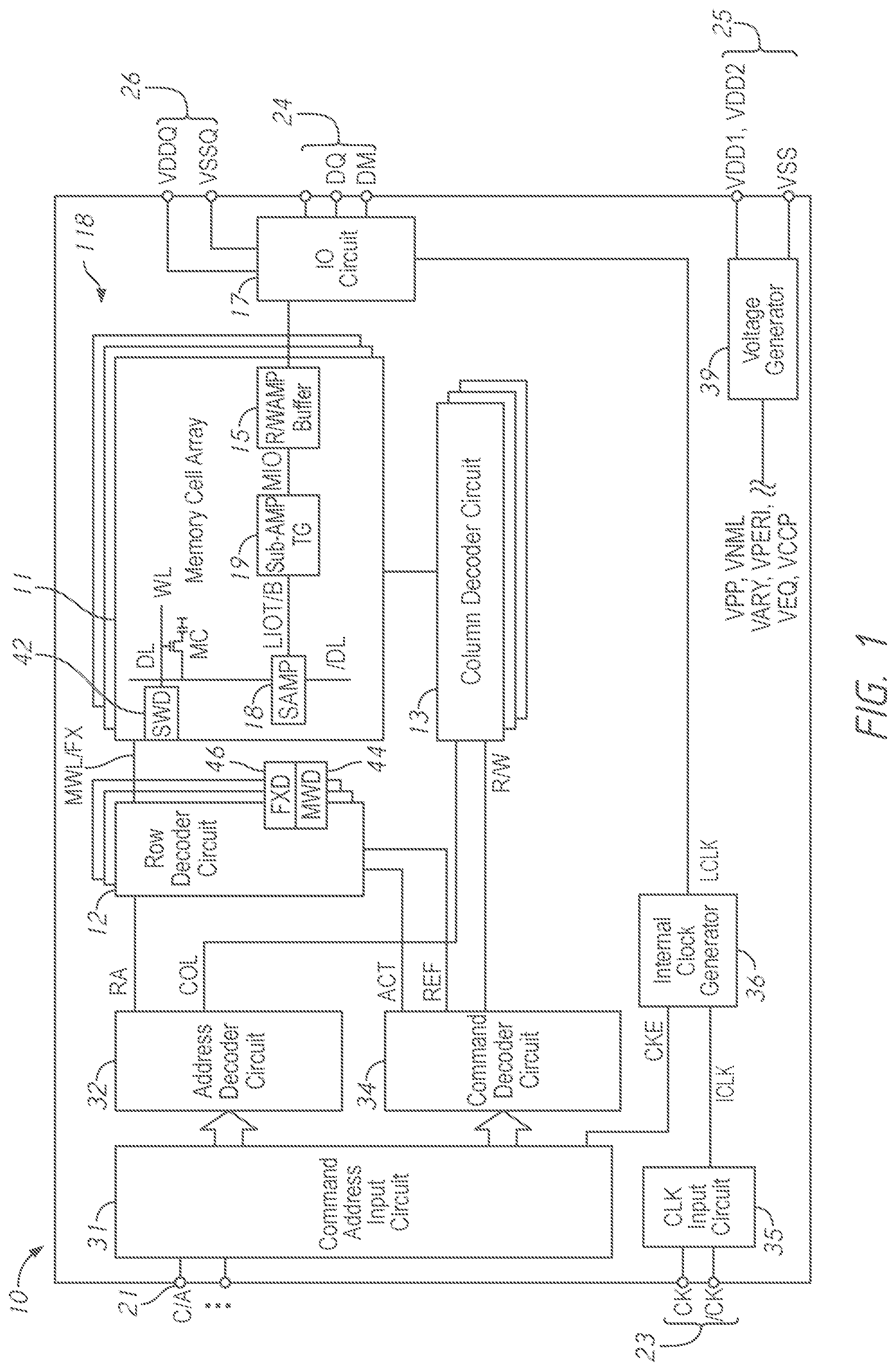
is a block diagram of a semiconductor device 10 according to some examples described in the disclosure. The semiconductor device 10 may be a dynamic random access memory (DRAM) in some embodiments of the disclosure. The semiconductor device 10 includes a memory cell array 11 . The memory cell array 11 includes a plurality of word lines WL and a plurality of data lines DL that intersect with each other, with memory cells (MC) disposed at the intersections. The WLs may be driven by respective subword drivers SWD. For clarity, only one WL, SWD, DL, and MC are shown in . A plurality of main word lines MWL and word driver lines FX may be provided to respective SWDs in the memory cell array 11 . For example, a selection of a main word line MWL and a word driver line FX is carried out by the row decoder circuit 12 , and the selection of the data line DL is carried out by a column decoder circuit 13 . In some examples, the word driver lines FX may be driven by respective word drivers FXD 46 . The main word lines MWL may be driven by respective main word drivers (MWD) 44 . For example, a memory device may have 128 main word lines and 128 main word drivers providing respective main word lines.
In some examples, the semiconductor device 10 may include multiple memory cell arrays 11 arranged in multiple memory banks. The semiconductor device 10 may also include multiple row decoder circuits 12 and multiple column decoder circuits, each coupled to a respective memory cell array 11 .
With further reference to , sense amplifiers 18 are coupled to corresponding data lines DL and coupled to local I/O line pairs LIOT/B. Local IO line pairs LIOT/B are coupled to main IO line pairs MIOT/B via transfer gates TG 19 which function as switches to read/write amplifiers and buffers 15 .
Turning to the explanation of a plurality of external terminals included in the semiconductor device 10 , the plurality of external terminals includes command and address terminals 21 , clock terminals 23 , data terminals 24 , and power supply terminals 25 and 26 . The command and address terminals 21 are supplied with command and address signals CA. The CA signals provided to the command and address terminals 21 include commands and addresses. Addresses included in the CA signals are transferred via a command/address input circuit 31 to an address decoder circuit 32 . The address decoder circuit 32 receives the addresses and supplies a decoded row address signal RA to the row decoder circuit 12 , and a decoded column address signal COL to the column decoder circuit 13 .
Commands included in the CA signals provided to the command and address terminals 21 are input to a command decoder circuit 34 via the command/address input circuit 31 . The command decoder circuit 34 decodes the commands to provide various internal command signals. For example, the internal commands may include a row command signal to select a word line and a column command signal, such as a read command or a write command, to select a data line.
When a activation command is issued and a row address is timely supplied with the activation command, and a column address is timely supplied with a read command, read data is read from a memory cell MC in the memory cell array 11 designated by these row address and column address. More specifically, the row decoder circuit 12 selects a main word line MWL, word driver line FX, and word line WL indicated by the row address RA so that the associated memory cell MC is subsequently connected to the data line DL. Further, when the memory cell MC is selected by the row address and the associated row is activated by the activation command, the main word line M W L may be active and the word driver line FX may be active. This results in the word line WL being active. Conversely, when the memory cell MC is not selected, e.g., in a precharge operation, the word driver line FX may be inactive, and the main word line MWL may also be inactive. This drives the word line WL to a non-active potential, e.g., off-state word line voltage VNWL. With further reference to , the read data DQ is output externally from the data terminals 24 via a read/write amplifier 15 and an input/output circuit 17 .
Similarly, when the activation command is issued and a row address are timely supplied with the activation command, and a column address is timely supplied with a write command, the input/output circuit 17 may receive write data DQ at the data terminals 24 . The write data DQ is supplied via the input/output circuit 17 and the read/write amplifier 15 to the memory cell array 11 and written in the memory cell MC designated by the row address and the column address.
The clock terminals 23 are supplied with external clock signals CK and/CK, respectively. These external clock signals CK and/CK are complementary to each other and are supplied to a clock input circuit 35 . The clock input circuit 35 receives the external clock signals CK and/CK and provides an internal clock signal ICLK. The internal clock signal ICLK is supplied to an internal clock generator 36 and thus a phase controlled internal clock signal LCLK is provided based on the received internal clock signal ICLK and a clock enable signal CKE from the command/address input circuit 31 . In a non-limiting example, a DLL circuit can be used as the internal clock generator 36 . The phase controlled internal clock signal LCLK is supplied to the input/output circuit 17 and is used as a timing signal for determining an output timing of the read data DQ.
The power supply terminals 25 are supplied with power supply voltages VDD1, VDD2, and VSS. These power supply voltages VDD1. VDD2, and VSS are supplied to an internal voltage generator circuit 39 . The internal voltage generator circuit 39 provides various internal voltages, such as, VPP, VARY, VPERI, VEQ, VCCP, and VNWL.
The internal potentials VCCP, VNWL are potentials to be mainly used in the row decoder circuit 12 , the main word drivers MWDs 44 and the word drivers FXDs 46 . For example, a word driver FXD, when selected based upon the address signal ADD, may be configured to drive a potential on the word driver line FX to a VCCP level corresponding to a high potential (e.g., 3.1 V). When a row is in pre-charge state, an associated subword driver, responsive to an inactive signal on a main word line (MWL) and an inactive signal on a word driver line (e.g., FXT, FXB), may be configured to pull down the word line (WL) to the internal voltage VNWL (e.g. a non-active potential, which may be a negative voltage).
The internal potential VARY and VEQ are potentials to be used by the sense amplifier 18 , transfer gates 19 and/or read/write amplifiers 15 . When the sense amplifier 18 is activated, the read data read out is amplified by driving one of the paired data lines to a VARY level with the other one being driven to a VSS level. The internal potential VPERI is used as a power supply potential for most of the peripheral circuits, such as the command/address input circuit 31 . By using the internal potential VPERI having a lower potential than the external potential VDD as the power supply potential of these peripheral circuits, it may be possible to reduce power consumption of the semiconductor device 10 .
The power supply terminals 26 are supplied with power supply voltages VDDQ and VSSQ. These power supply voltages VDDQ and VSSQ are supplied to the input/output circuit 17 . The power supply voltages VDDQ and VSSQ may be the same voltages as the power supply voltages VDD2 and VSS that are supplied to the power supply terminals 25 , respectively. However the dedicated power supply voltages VDDQ and VSSQ may be used for the input/output circuit 17 so that power supply noise generated by the input/output circuit 17 does not propagate to the other circuit blocks of device 10 .
is a schematic diagram of a portion of a memory bank 200 according to some examples described in the disclosure. In some embodiments of the disclosure, the portion of the memory bank 200 may be included in one bank of the multiple banks in the memory cell array 11 of .
The portion of the memory bank 200 may include multiple word lines 210 , each provided by a respective subword driver SWDj 216 . For example, a word line 214 may be provided by a corresponding subword driver SWD 5 associated with a main word line driven by a main word driver MWD 1 and also associated with a word driver line 202 (e.g., FX 5 ) associated with a word driver 208 . In other words, for each subword driver, a corresponding main word line MWL and word driver line FX and non-active potential (e.g., off-state word line voltage VNWL) are provided. The signals on the main word lines MWLs and the word driver lines FXs may be provided by main word drivers MWD 0 -N and word drivers FXDs 204 , based upon the row address RA.
A main word line MWL may extend over array regions of a respective memory mat to provide the main word signal to the subword driver rows SWD 0 - 7 of the memory mat to activate those subword drivers SWD 0 - 7 . That is, when a main word driver MWD is activated, it may provide active main word signals to all the subword drivers SWD 0 - 7 of the mat. As will be described below, a word driver line FX may include FXT and FXB that transmits a signal complementary to a signal of the FXT. In some examples, when the FXT is active, the FXB line is inactive. Conversely, the FXB may be active while the FXT is inactive. Each word driver line 202 of word driver FXD 204 provides word driver lines to at least one subword driver SWD in each mat. In the example shown in , the word driver FXD 204 includes even word drivers 206 and odd word drivers 208 . The even word drivers 206 provide respective word driver lines to even-numbered subword drivers SWIX), SWD 2 , SWD 4 , and SWD 6 , of each memory mat and odd word drivers 208 provide respective word driver lines to odd-numbered subword drivers SWD 1 , SWD 3 , SWD 5 , and SWD 7 of each memory mat. However other arrangements may be used in other examples. In the example shown in , each word driver line of the word driver 204 may be coupled to a corresponding subword driver SWD 0 - 7 in each memory mat. For example, FX line 5 may be coupled to the subword driver SWD 5 of each memory mat.
In the example operation shown in , a row address RA has indicated MWD 1 should be activated and odd word driver 208 associated with word driver line FX 5 should be activated. As shown by the shaded regions 212 , word lines 210 associated with the inactive main word drivers MWD 0 , MWDn remain inactive, even the subword lines associated with word driver line FX 5 are active. However, among the word lines 222 that are associated with activated MWD 1 , the word line 214 driven by subword driver SWD 5 associated with activated MWD 1 and FX 5 is activated. By way of example, an activated MWD may be configured to provide an active signal on the associated main word line, and an activated word driver FXD may be configured to provide an active signal on the word driver line (e.g., FXT, FXB). Similarly, an activated subword driver may be configured to provide an active signal on the associated word line. Thus, a selected word line WL of the selected memory mat associated with MWD 1 is driven to the active potential by the corresponding activated subword driver SWD 5 .
In some examples, the other subword drivers SW D of the selected memory mat drive the respective unselected word lines WL to the non-active potential (e.g., VNWL) to remain inactive. Subword drivers SWD of unselected memory mats MAT (e.g., memory mats associated with MWD 0 and MWDn) remain deactivated, and the word lines WL of the unselected memory mats MAT are not provided a voltage, or instead, provided with a non-active potential (e.g., VNWL) in some examples. Whereas a subword driver SWD is coupled to a word driver FXD and a main word driver MWD, in order for a word line WL associated with the subword driver SWD to be activated, both the associated word driver FXD and the main word driver MWD must be activated.
is a schematic diagram of a conventional subword driver and a memory cell. As shown in , the output of a subword driver 302 is coupled to a word line WL, which is coupled to memory cell 312 . The memory cell 312 includes at least a transistor and a capacitor. The word line WL is connected to the gate of the transistor and the data line DL is connected to the drain/source (drain or source) of the transistor. The memory cell is capable of storing 1-bit data. The memory cell 312 is coupled to a sense amplifier 310 configured to sense a signal of the memory cell 312 on the data line DL and drive the signal to a desired voltage.
The subword driver 302 includes two transistors of different conductivity types (e.g., a p-channel type transistor 304 and an n-channel type transistor 306 ) serially coupled at the word line WL. A main word line MWL is coupled to the gates of the transistors 303 and 306 . A word driver line FXT is coupled to the drain/source of the transistor 304 , and the non-active potential VNWL is provided to the drain/source of the transistor 306 . The word line WL is also coupled to the non-active potential VNWL through an n-channel type transistor 308 . A word driver line FXB is coupled to the gate of the transistor 308 .
The word line of the memory cell 312 is coupled to the subword driver 302 , which operates responsive to the signals on the main word line signal MWL and the word driver line FXT. In operation, the transistors 304 and 306 are configured to provide an active/inactive signal on the word line WL. The n-channel type transistor 308 is used to prevent unselected word lines from floating. For example, when the main word line MWLB is active low, the transistor 304 is turned on and the transistor 306 is turned off. If FXT is inactive, the FXB will be active to turn on the transistor 308 , which pulls down the potential at the word line WL to VNWL, preventing the word line from floating. As shown in , the subword driver 302 in the conventional circuit includes at least three transistors.
is a plan view of an example layout diagram of subword drivers showing active regions according to some examples described in the disclosure. In some examples, layout 400 may include a gate layer overlaid on a p-channel type area 402 and an n-channel type area 404 to form p-channel type or n-channel type transistors. As shown in , the p-channel type area has multiple sub-regions, e.g., 406 A-D, each extending in a direction 410 B. The n-channel type area has multiple sub-regions, e.g., 409 A-D, each extending in the direction 410 B. It is appreciated that, although only four sub-regions are shown, both the p-channel type area and n-channel type area may have any suitable number of sub-regions.
In some examples, the gate layer may include multiple gate electrodes, each extending in a direction 410 A that is perpendicular to the direction 410 B. Each gate electrode may be coupled to a respective main word line MWLB. In , four gate electrodes respectively for main word lines MWLBn−1, MWLBn, MWLBn+1, and MWLBn+2 are shown, where “n” is an integer. Although the layout 400 shows only a portion of the memory device, it is appreciated that additional gate electrodes for other main word lines may be included.
With further reference to , the layout 400 may also include contacts for active regions or gate layers. As shown, diffusion contacts may be arranged in an active region on each side of a gate. In the p-channel type area 402 , gate electrodes may overlap with active regions including P+ diffusion materials to form respective p-channel type transistors. For example, the respective p-channel type transistors may be the p-channel type transistor 304 in . For example, p-channel type transistors 424 A and 424 B may be formed over respective gate electrodes in a P+ diffusion sub-region 406 B. Also, p-channel type transistors 424 C and 424 D may be formed over respective gate electrodes in a P+ diffusion sub-region 406 C. A contact on the active region may be coupled to a word line WLm+j or a word driver line (e.g., FXTj), where “m” and “j” are integers. A FXT word driver line (e.g., FXT 0 , FXT 1 , FXT 2 , FXT 3 ) is connected to a common source/drain between adjacent main word lines (MWLB).
In some embodiments, p-channel type transistor 424 A is formed over the gate electrode associated with MWLBn+2 with two contacts on each side of the gate electrode, where the two contacts are coupled to a word line (e.g., WLm+16) and a word driver line (e.g., FXT 0 ), respectively. Also, p-channel type transistor 424 B is formed over the gate electrode associated with MWLBn+1 with two contacts on each side of the gate electrode, where the two contacts are coupled to a word line (e.g., WLm+2) and a word driver line (e.g., FXT 0 ), respectively. Similarly, p-channel type transistor 424 C is formed over the gate electrode associated with MWLBn+1 with two contacts on each side of the gate electrode, where the two contacts are coupled to a word line (e.g., WLm+6) and a word driver line (e.g., FXT 4 ), respectively. Additionally, p-channel type transistor 424 D is formed over the gate electrode associated with MWLBn with two contacts on each side of the gate electrode, where the two contacts are coupled to a word line (e.g., WLm−4) and a word driver line (e.g., FXT 4 ), respectively.
In the embodiment of , FXT 0 and FXT 2 are coupled to respective common sources/drains between adjacent gate electrodes associated with MWLBn−1 and MWLBn. FXT 0 and FXT 2 are also coupled to respective common sources/drains between adjacent main word lines MWLBn+1 and MWLBn+2. FXT 4 and FXT 6 are coupled to respective common drains/sources between adjacent main word lines MWLBn and MWLBn+1. For each gate, on the opposite side from the common source/drain, a respective word line is coupled to the drain/source. Along the gate electrode associated with main word line MWLBn+1, a word line WLm+2 is coupled to the drain of the transistor 424 B, opposite the common source with transistor 424 A coupled to FXT 0 . The drain of the transistor 424 A is coupled to a word line WLm+16, and the gate of the transistor 424 A is coupled the gate electrode associated with main word line MWLBn+2. Also, along the gate electrode associated with MWLBn, a word line WLm−4 is coupled to the drain of the transistor 424 D, opposite the common source with transistor 424 C coupled to FXT 4 . Similarly, along the gate electrode associated with main word line MWLBn+1, a word line WLm+6 is coupled to the drain of the transistor 424 C. This pattern repeats for additional word lines.
Each sub-region of the multiple sub-regions, e.g., 406 A-D may include active regions. For example, in , the sub-region 406 B may include an active region 401 A and the sub-region 406 C may include an active region 401 B. The active region 401 A may include drains/sources (e.g., drain and source regions) and channel regions between the respective drains and sources for the transistors 424 A and 424 B. The active region 401 A includes end portions 4012 A and 4013 A, and a center portion 4011 A between the end portions. One of the end portions 4012 A may include the drain of the transistor 424 A coupled to the word line WLm+16. Another end portion 4013 A of the end portions may include the drain of the transistor 424 B coupled to the word line WLm+2. The center portion 4011 A of the active region 401 A may include the common source between the transistors 424 A and 424 B coupled to FXT 0 . The active region 401 B includes end portions 4012 B and 4013 B, and a center portion 4011 B between the end portions. One end portion 4012 B of the end portions may include the drain of the transistor 424 C coupled to the word lines WLm+6. Another end portion 4013 B of the end portions may include the drain of the transistor 424 D coupled to the word line WLm−4. The center portion 4011 B of the active region 401 B may include the common source between the transistors 424 A and 424 B coupled to FXT 4 . The drain of the transistor 424 B is included in the end portion 4013 A of the active region 401 A and the source of the transistor 424 C is included in the center portion 4011 B of the active region 401 B. The drain of the transistor 424 B and the source of the transistor 424 C are disposed along the same side of the gate electrode associated with the main word line MWLBn+1 and on the sub-regions 406 B and 406 C adjacent to each other, respectively. Thus, the end portion 4013 A including the drain of the transistor 424 B and the center portion 4011 B including the source of the transistor 424 C may be adjacent to each other.
A width of the center portion 4011 B of the active region 401 B may be shorter than a width of the end portions 4012 B and 4013 B of the active region 401 B. As a result, a distance between the end portion 4013 A of the active region 401 A including the drain of the transistor 424 B and the center portion 4011 B of the active region 401 B including the source of the transistor 424 C may be greater than a distance between the end portion 4013 A of the active region 401 A including the drain of the transistor 424 B and the end portion 4012 B of the active region 401 B including the drain of the transistor 424 C.
In the n-channel type area 404 , the gate electrodes overlay with N+ diffusion sub-regions to form respective n-channel type transistors. In some embodiments, the respective n-channel type transistors may include the n-channel type transistor 306 and the n-channel type transistor 308 in . A contact on the active region may be coupled to a word line WLm+i or a non-active potential VNWL, where “i” is an integer. In other words, non-active potential VNWL and respective word lines are coupled to the source/drain of each transistor. A gate of each n-channel transistor may be coupled to a non-active potential VNWL, if the n-channel transistor functions as the n-channel type transistor 306 . A gate of each n-channel transistor may be coupled to a FXB word driver line (e.g., FXB 0 , FXB 1 , FXB 2 , FXB 3 ) that transmits a complementary signal of the FXT word driver line (e.g., FXT 0 , FXT 1 , FXT 2 , FXT 3 ), if the n-channel transistor functions as the n-channel type transistor 308 .
In some embodiments, transistor 426 D is formed and coupled to main word line MWLBn at the gate, and transistor 428 D is formed and coupled to FXB 4 at the gate. The transistors 426 D and 428 D are further coupled to VNWL and WLm−4 at the respective sources/drains. Transistor 426 C is formed and coupled to main word line MWLBn+1 at the gate, and transistor 428 C is formed and coupled to FXB 4 at the gate. The transistors 426 C and 428 C are further coupled to VNWL and WLm+6 at the respective sources/drains. Transistor 426 B is formed and coupled to main word line MWLBn+1 at the gate, and transistor 428 B is formed and coupled to FXB 0 at the gate. The transistors 426 B and 428 B are further coupled to VNWL and WLm+2 at the respective sources/drains. Transistor 426 A is formed and coupled to main word line MWLBn+2 at the gate, and transistor 428 A is formed and coupled to FXB 0 at the gate. The transistor 426 A and 428 A are further coupled to VNWL and WLm+16 at the respective sources/drains. This pattern repeats for additional word lines.
The transistors 424 A, 426 A and 428 A may be included in a subword driver, as the subword driver 302 in . For example, the transistor 424 A, 426 A and 428 A may be included as the transistors 304 , 306 and 308 of , respectively, to form a subword driver that receives a main word line signal MWLBn+2 and complementary word line signals FXT 0 /FXB 0 as input signals to either active or deactivate the word line WLm+16. Similarly, the transistors 424 B, 426 B and 428 B may be included as the transistors 304 , 306 and 308 of , respectively, to form a subword driver that receives a main word line signal MWLBn+1 and complementary word line signals FXT 0 /FXB 0 as input signals to either active or deactivate the word line WLm+2. The transistors 424 C, 426 C and 428 C may be included as the transistors 304 , 306 and 308 of , respectively, to form a subword driver that receives a main word line signal MWLBn+1 and complementary word line signals FXT 4 /FXB 4 as input signals to either active or deactivate the word line WLm+6. The transistors 424 D, 426 D and 428 D may be included as the transistors 304 , 306 and 308 of , respectively, to form a subword driver that receives a main word line signal MWLBn+1 and complementary word line signals FXT 4 /FXB 4 as input signals to either active or deactivate the word line WLm−4.
In the example in , even-numbered word lines are shown in the layout 400 , which may implement the subword driver 216 of or the subword driver 302 of . With reference to , 3 and 4 , it is appreciated that the circuit implemented in the layout 400 may implement one or more subword drivers 302 . For example, for a given memory cell array (e.g., a memory cell array 11 of ), subword drivers associated with even-numbered word lines for the given memory cell array may be laid out in a similar manner as shown in and arranged adjacent to one side of the memory cell army. Similarly, subword drivers associated with odd-numbered word lines for the memory cell array may be laid out in a similar manner as shown in and arranged adjacent to another side of the memory cell array. In some embodiments of the disclosure, the layout of the subword drivers associated with the odd numbered word lines may be arranged in a mirror arrangement relative to the subword drivers associated with the even numbered word lines.
is a plan view of an example layout diagram of portions of subword drivers showing active regions according to some examples described in the disclosure. In some examples, layout 500 of the portions of subword drivers may include active regions 501 A and 501 B that extend in a direction 510 B. Each active region of the active regions 501 A and 501 B implements portions of multiple subword drivers. Each subword driver of the multiple subword drivers may be one of subword drivers 216 in the portion of the memory bank 200 of , or a subword driver 302 of .
An active region may include one or more drains, sources and channels. For example, an active region may include P+ diffusion materials to form p-channel type transistor. The active regions 501 A and 501 B include P+ diffusion materials and implement p-channel type transistors in the subword drivers. For example, the active region 501 A may implement p-channel type transistors 520 A and 520 B, and the active region 501 B may implement p-channel type transistors 520 C and 520 D. In some embodiments, the p-channel type transistors 520 A, 520 B, 520 C and 520 D may be the p-channel type transistors 424 A, 424 B, 424 C and 424 D of . Each p-channel type transistor of the p-channel type transistors 520 A, 520 B, 520 C and 520 D may include a source and a drain. For example, the p-channel type transistor 520 A may include a drain 503 A having a contact and a source 504 A having a contact included in the active region 501 A. The p-channel type transistor 520 B may include a drain 503 B having a contact and the source 504 A having the contact shared with the p-channel type transistor 520 A included in the active region 501 A. The p-channel type transistor 520 B may further include a channel region between the drain 503 B and the source 504 A. The channel region may include a portion 505 A of a side of the drain 503 B and a portion 505 B of a side of the source 504 A. The p-channel type transistor 520 C may include a drain 503 C having a contact and a source 504 B having a contact. The p-channel type transistor 520 C may further include a channel region between the drain 503 C and the source 504 B. The channel region may include a portion 505 C of a side of the drain 503 c and a portion 5051 ) of a side of the source 504 B. The p-channel type transistor 5201 ) may include a drain 503 D having a contact and the source 504 B having the contact shared with the p-channel type transistor 520 C. In some embodiments, the drain 503 B may be arranged adjacent to the portion 505 D of the channel region of the p-channel type transistor 520 C of the side of the source 504 B. The drain 503 C may be arranged adjacent to the portion 505 B of the channel region of the p-channel type transistor 520 B of the side of the source 504 A.
In some examples, layout 500 of subword drivers may include gate electrodes 502 A 502 B and 502 C. In some embodiments, each gate electrode of the gate electrodes 502 A, 502 B and 502 C extends in a direction 510 A that is perpendicular to the direction 510 B on the plan view of . In the layout 500 , each gate electrode of the gate electrodes 502 A, 502 B and 502 C may overlap with at least portions of active regions 501 A and 501 B including P+ diffusion materials to form respective p-channel type transistors. For example, the gate electrodes 502 A and 502 B may overlap with portions of the active region 501 A and the gate electrodes 502 B and 502 C may overlap with portions of the active region 501 B. In some embodiments, portions of the active region 501 A may overlap with the gate electrodes 502 A and 502 B, and portions of the active region 50 L B may overlap with the gate electrodes 502 B and 502 C. In the layout 500 , each gate electrode of the gate electrodes 502 A, 502 B and 502 C may be disposed in parallel. The source 504 A may be disposed between the gate electrodes 502 A and 502 B. The source 504 B may be disposed between the gate electrodes 502 B and 502 C.
Each of the p-channel type transistors 520 A, 520 B, 520 C and 520 D may include a gate. For example, the p-channel type transistor 520 A may include a gate included in the gate electrode 502 A that is between the drain 503 A and the source 504 A. The p-channel type transistor 520 B may include a gate included in the gate electrode 502 B that is between the drain 503 B and the source 504 A. The p-channel type transistor 520 C may include a gate included in the gate electrode 502 B that is between the drain 503 C and the source 504 B. The p-channel type transistor 520 D may include a gate included in the gate electrode 502 C that is between the drain 503 D and the source 504 B.
In some embodiments, each active region of the active regions 501 A and 501 B may have a center portion and two end portions disposed at ends of the center portion in the direction 510 B. Each center portion may include a source and each end portion may include a drain. For example, the end portions 5012 A, 5013 A, 5012 B, and 5013 B may include drains 503 A, 503 B, 503 C, and 503 D of the transistors 520 A, 520 B, 520 C and 520 D, respectively. The center portion 5011 A may include the source 504 A shared by the transistors 520 A and 520 B and the center portion 501 B may include the source 504 B shared by the transistors 520 C and 520 D. A width of each contact of the sources 504 A and 504 B may be smaller than widths W 1 and W 3 of each respective center portion of the center portions 5011 A and 50111 B. In some embodiments, W 1 and W 3 may be the same.
In each active region, the widths of the end portions are greater than the width of the center portion. The active region 501 A may include the center portion 5011 A, the end portion 5012 A disposed at an end 5014 A of the center portion 5011 A and another end portion 5013 A disposed at another end 5015 A of the center portion 5011 A. The end portion 5012 A and the center portion 5011 A are in contact with each other at the end 5014 A of the center portion 5011 A in the direction 510 A. The center portion 5011 A and the end portion 5013 A are in contact with each other at the other end 5015 A of the center portion 5011 A in the direction 510 A. A width of the end portion 5012 A may be defined by a distance between sides of the end portion 5012 A that extend in the direction 510 B. A width of the center portion 5011 A W 1 may be defined by a distance between sides of the center portion 5011 A that extend in the direction 510 B. A width W 2 of the end portion 5013 A may be defined by a distance between sides of the end portion 5013 A that extend in the direction 510 B. The width W 2 of the end portion 5013 A may be greater than the width W 1 of the center portion 5011 A. The width W 1 of the portion 505 B of the channel region of the transistor 520 B of the side of the source 504 A is smaller than the width W 2 of the portion 505 A of the transistor 520 B of the channel region of the side of the drain 503 B. In another example, the active region 5011 B may include a center portion 50111 B and an end portion 5012 B disposed at an end 5014 B of the center portion 50111 B and another end portion 5013 B disposed at another end 5015 B of the center portion 50111 B. The end portion 5012 B and the center portion 5011 B are in contact with each other at the end 5014 B of the center portion 5011 B that extends in the direction 510 A. The center portion 5011 B and the end portion 5013 B are in contact with each other at the other end 5015 B of the center portion 5011 B that extends in the direction 510 A. A width W 4 of the end portion 5012 B may be defined by a distance between sides of the end portion 5012 B. A width W 3 of the center portion 5011 B may be defined by a distance between sides of the center portion 5011 B that extend in the direction 510 B. A width of the end portion 5013 B may be defined by a distance between sides of the end portion 5013 B that extend in the direction 510 B. The width W 4 of the end portion 5012 B may be greater than the width of the center portion 5011 B. The width W 3 of the portion 505 D of the channel region of the transistor 520 C of the side of the source 504 B is smaller than the width W 4 of the portion 505 C of the channel region of the transistor 520 C of a side of the drain 503 C.
In some embodiments, it may be desired to increase a distance L 2 between each contact of each drain and its adjacent gate electrode to prevent leakage currents due to the gate induced drain leakage (GIDL). Each gate electrode of the gate electrodes 502 A, 502 B and 502 C may have recess regions on sides that extend in the direction 510 A. For example, the gate electrode 502 A includes a recess region 5021 A on a side that extends in the direction 510 A. The contact of the drain 503 A may be disposed within the recess region 5021 A and may maintain a distance from the gate electrode 502 A. Thus, the recess region 5021 A may provide a distance L 2 between the contact of the drain 503 A and the gate electrode 502 A. The gate electrode 502 B may include a recess region 5021 B on a side that extends in the direction 510 A. The contact of the drain 503 B may be disposed within the recess region 5021 B and may maintain a distance L 2 from the gate electrode 502 B. Thus, the recess region 5021 B may provide a distance L 2 between the contact of the drain 503 B and the gate electrode 502 B. The gate electrode 502 B may include another recess region 5021 C on another side that extends in the direction 510 A. The contact of the drain 503 C may be disposed within the recess region 5021 C and may maintain a distance L 2 from the gate electrode 502 B. Thus, the recess region 5021 C may provide a distance L 2 between the contact of the drain 503 C and the gate electrode 502 B. The gate electrode 502 C includes a recess region 5021 D on a side that extends in the direction 510 A. The contact of the drain 503 D may be disposed within the recess region 5021 D and may maintain a distance L 2 from the gate electrode 502 C. The recess region 50211 D may provide a distance L 2 between the contact of the drain 503 D and the gate electrode 502 C. Thus, active regions having end portions with a greater width that provide the greater distance L 2 may prevent the GIDL between drains and adjacent gate electrodes.
In some embodiments, it may be desired to increase the distance between adjacent active regions overlapped by the same gate electrode to prevent leakage currents due to the hot electron induced punch-through (HEIP). For example, the width W 2 of the end portion 5013 A of the active region 501 A may include an overlapping width L 1 with the gate electrode 502 B next to the recess region 5021 B and include the width L 2 between the contact of the drain 503 B and sides of the recess region 5021 B that extend in the direction 510 B. The width of the center portion 5011 B W 3 of the active region 501 B may be smaller than the width W 4 of the end portion 5012 B of the active region 501 B. The end portion 5013 A of the active region 501 A and the center portion 5011 B of the active region 501 B may be adjacent to each other on the side of the gate electrode 502 b having the recess region 5021 B. A distance L 3 between the end portion 5013 A of the active region 501 A and the center portion 5011 B of the active region 5011 B may be provided. The distance L 3 may be provided by having the width W 3 of the center portion 5011 B of the active region 5011 B including the portion 505 D of the channel region of the transistor 520 C smaller than the width W 4 of the end portion 5012 B of the active region 501 B including the portion 505 C of the channel region of the transistor 520 C. Increasing the distance 13 by having a smaller width W 3 of the center portion 5011 B may prevent hot electrons around the drain of 503 B of the p-channel type transistor 520 B from affecting the source 504 B of the adjacent p-channel type transistor 520 C to lower a threshold voltage (Vth) of the p-channel type transistor 520 C. Thus, active regions having center portions with a less width to provide the greater distance L 3 may prevent the HEIP between drains and sources of adjacent transistors.
Semiconductor devices of provide various advantages in reducing leakage currents over conventional subword driver layouts. For example, active regions having end portions with a greater width allow large recess regions of gate electrodes overlapping drains. The large recess regions provide a greater distance between the drains and the gate electrodes. The greater distance between the drains and the gate electrodes described above as the embodiments of the current disclosure may reduce leakage currents, such as the GIDL, between the drains and the gate electrodes. For further example, the end portions of each active region have a width greater than a width of a center portion between the end portions. This configuration may provide a greater distance between an end portion of one active region including a drain and a center portion of another active region adjacent to the active region that includes a source. The greater distance between the end portion of the one active region and the center portion of the other active region described above as the embodiments of the current disclosure may reduce leakage currents between the drain in the one active region and the source of the other active region due to the HEIP.
From the foregoing it will be appreciated that, although specific embodiments of the disclosure have been described herein for purposes of illustration, various modifications may be made without deviating from the spirit and scope of the disclosure. Accordingly, the scope of the disclosure should not be limited any of the specific embodiments described herein.
Figures (5)
Citations
This patent cites (2)
- US20130058155
- US20180166119