Pixel Circuit and Image Sensor Including Thereof
Abstract
An image sensor includes a pixel array including a first shared pixel and a second shared pixel that are adjacent to each other in a row direction. The first shared pixel includes two or more photo diodes in a first row and two or more photo diodes in a second row, and the first shared pixel includes a first floating diffusion region shared by the photo diodes of the first shared pixel. The second shared pixel includes two or more photo diodes in the first row and two or more photo diodes in the second row, and the second shared pixel includes a second floating diffusion region shared by the photo diodes of the second shared pixel.
Claims (18)
1. An image sensor comprising: a first shared pixel comprising first to fourth subpixels configured to share a first floating diffusion area; a second shared pixel disposed close to the first shared pixel in a first direction, and comprising fifth to eighth subpixels configured to share a second floating diffusion area; and a row driver connected to the first to fourth subpixels respectively through first to fourth transmission control signal lines, and to the fifth to eighth subpixels respectively through fifth to eighth transmission control signal lines, and configured to control exposure time in response to respective signals of the first to eighth transmission control signal lines for the first to eighth subpixels, wherein the image sensor is configured such that, in a first operation mode, the first to fourth subpixels are exposed for a long time, and the fifth to eighth subpixels are exposed for a short time, wherein the first to eighth transmission control signal lines are different from each other, and wherein the image sensor is configured such that, in a second operation mode, at least one of the first to fourth subpixels is exposed for a short time, others of the first to fourth subpixels are exposed for a long time, at least one of the fifth to eighth subpixels is exposed for a short time, and others of the fifth to eighth subpixels are exposed for a long time.
8. A pixel array comprising: a first shared pixel comprising first subpixels configured to share a first floating diffusion area; a second shared pixel disposed directly adjacent to the first shared pixel in a first direction, and comprising second subpixels configured to share a second floating diffusion area; a third shared pixel disposed directly adjacent to the first shared pixel in a second direction orthogonal to the first direction, and comprising third subpixels configured to share a third floating diffusion area; and a fourth shared pixel disposed directly adjacent to the third shared pixel in the first direction, and comprising fourth subpixels configured to share a fourth floating diffusion area, wherein each of the first subpixels of the first shared pixel is respectively connected to first transmission control signal lines, and is configured to be exposed to light in response to a respective signal of the first transmission control signal lines, wherein each of the second subpixels of the second shared pixel is respectively connected to second transmission control signal lines, and is configured to be exposed to light in response to a respective signal of the second transmission control signal lines, wherein the third subpixels of the third shared pixel, and the fourth subpixels of the fourth shared pixel are configured to: share third transmission control signal lines, and be exposed to light in response to respective signals of the third transmission control signal lines, and wherein the first to third transmission control signal lines are different from each other.
16. An image sensor comprising: a first shared pixel configured to share a first floating diffusion area, and comprising first to fourth subpixels respectively connected to first to fourth transmission signal lines; a second shared pixel disposed close to the first shared pixel in a first direction, configured to share a second floating diffusion area, and comprising fifth to eighth subpixels respectively connected to fifth to eighth transmission signal lines; a third shared pixel disposed close to the second shared pixel in the first direction, configured to share a third floating diffusion area, and comprising ninth to twelfth subpixels respectively connected to the first to fourth transmission signal lines; and a timing controller configured to control exposure of the first and second shared pixels in units of any one of shared pixels and subpixel units by using signals of the first to eighth transmission signal lines according to an operation mode, wherein the first to eighth transmission signal lines are different from each other, and wherein, in a first operation mode, the timing controller is configured to control the first and third shared pixels to be exposed for a long time by using signals of the first to fourth transmission signal lines, and the second shared pixel to be exposed for a short time by using signals of the fifth to eighth transmission signal lines.
Show 15 dependent claims
2. The image sensor of claim 1 , further comprising: a third shared pixel disposed close to the first shared pixel in a second direction orthogonal to the first direction, and comprising ninth to twelfth subpixels configured to share a third floating diffusion area; and a fourth shared pixel disposed close to the third shared pixel in the first direction, and comprising thirteenth to sixteenth subpixels configured to share a fourth floating diffusion area, wherein the row driver is: connected to the ninth to twelfth subpixels respectively through ninth to twelfth transmission control signal lines, and connected to the thirteenth to sixteenth subpixels respectively through the ninth to twelfth transmission control signal lines, and configured to control exposure time in response to signals of the ninth to twelfth transmission control signal lines for the ninth to sixteenth subpixels, and wherein, the image sensor is configured such that, in the first operation mode, the ninth to sixteenth subpixels are exposed for a long time.
3. The image sensor of claim 1 , further comprising: a third shared pixel disposed close to the second shared pixel in the first direction, the third shared pixel comprising ninth to twelfth subpixels configured to share a third floating diffusion area, wherein the row driver is connected to the ninth to twelfth subpixels respectively through the first to fourth transmission control signal lines, and wherein, the image sensor is configured such that, in the first operation mode, the ninth to twelfth subpixels are exposed for a short time.
4. The image sensor of claim 1 , wherein the row driver is: connected to the first and second shared pixels through a selection signal line and a reset signal line, configured to select a shared pixel of the first and second shared pixels in response to a signal of the selection signal line, and configured to reset a floating diffusion area of the first and second floating diffusion areas in response to a signal of the reset signal line.
5. The image sensor of claim 1 , wherein each of the first to fourth subpixels comprises a first color filter, and wherein each of the fifth to eighth subpixels comprises a second color filter.
6. The image sensor of claim 1 , wherein the first shared pixel is connected to a first column output line, and wherein the second shared pixel is connected to a second column output line.
7. The image sensor of claim 1 , further comprising: a timing controller configured to control the row driver to perform exposure in units of shared pixels in the first operation mode, and perform exposure in units of subpixels in a second operation mode.
9. The pixel array of claim 8 , wherein the pixel array is configured such that the first shared pixel is exposed for a first time through the first transmission control signal lines, the second shared pixel is exposed for a second time through the second transmission control signal lines, and the third and fourth shared pixels are exposed for a third time through the third transmission control signal lines.
10. The pixel array of claim 9 , wherein the third time is the same as the first time.
11. The pixel array of claim 9 , wherein the third time is the same as the second time.
12. The pixel array of claim 9 , wherein each of the first subpixels comprises a first color filter, each of the second subpixels and each of the third subpixels comprises a second color filter, and each of the fourth subpixels comprises a third color filter.
13. The pixel array of claim 12 , wherein the first color filter is a blue filter, the second color filter is a green filter, and the third color filter is a red filter.
14. The pixel array of claim 8 , wherein the first and second shared pixels are configured to: share a first selection signal line and a first reset signal line, select a shared pixel of the first and second shared pixels in response to a signal of the first selection signal line, and reset a floating diffusion area of the first and second floating diffusion areas in response to a signal of the first reset signal line, and wherein the third and fourth shared pixels are configured to: share a second selection signal line and a second reset signal line, select a shared pixel of the third and fourth shared pixels in response to a signal of the second selection signal line, and reset a floating diffusion area of the third and fourth floating diffusion areas in response to a signal of the second reset signal line.
15. The pixel array of claim 8 , wherein each of the first to fourth shared pixels comprises 3×3 or 4×4 subpixels.
17. The image sensor of claim 16 , wherein, in a first operation mode, the timing controller is configured to control the first shared pixel to be exposed for a long time by using signals of the first to fourth transmission signal lines, and the second shared pixel to be exposed for a short time by using signals of the fifth to eighth transmission signal lines.
18. The image sensor of claim 16 , wherein, in a second operation mode, the timing controller is configured to: by using signals of the first to fourth transmission signal lines, control at least one of the first to fourth subpixels to be exposed for a long time, and others of the first to fourth subpixels to be exposed for a short time, and by using signals of the fifth to eighth transmission signal lines, control at least one of the fifth to eighth subpixels to be exposed for a long time, and others of the fifth to eighth subpixels to be exposed for a short time.
Full Description
Show full text →
CROSS-REFERENCE TO RELATED APPLICATION
This U.S. non-provisional patent application is a Continuation of U.S. patent application Ser. No. 16/699,430, filed on Nov. 29, 2019, which is a Continuation of U.S. patent application Ser. No. 15/844,279, filed on Dec. 15, 2017, U.S. Pat. No. 10,547,800, which claims priority under 35 U.S.C. § 119 to Korean Patent Application No. 10-2017-0064388, filed on May 24, 2017, in the Korean Intellectual Property Office, the disclosure of each of which is incorporated herein in its entirety by reference.
BACKGROUND
The present disclosure relates to an image sensor, and more particularly, to an image sensor including a pixel circuit including a shared pixel.
Image sensors that capture an image and convert it into an electrical signal are used in cameras installed in, for example, vehicles, security devices, and robots as well as in consumer electronics such as digital cameras, cameras for mobile phones, and portable camcorders. Such image sensors may include a pixel array, and each pixel included in the pixel array may include a photo detecting device. The photo detecting device may generate an electrical signal depending on intensity of the absorbed light.
Sizes of pixels of image sensors have been gradually reduced to improve resolution, but image quality needs to be fully guaranteed even with the reduced pixel size. In relation to quality of an image sensor, a dynamic range can be problematic, and when a wide dynamic range (WDR) is provided, both a bright region and a dark region of an image may be expressed in detail.
SUMMARY
The present disclosure provides a pixel circuit which is easily embodied and provides a wide dynamic range under various illumination conditions, and provides an image sensor including the pixel circuit.
According to an aspect of the inventive concept, there is provided an image sensor including a pixel array including a plurality of shared pixels arranged in rows and columns, wherein a first shared pixel and a second shared pixel of the shared pixels are adjacent to each other in a row direction and connected to one selection signal line; and a timing controller configured to control a generation of pixel signals from the first shared pixel and the second shared pixel based on an operation mode of the image sensor, wherein the first shared pixel includes two or more photo diodes in a first row and two or more photo diodes in a second row adjacent to the first row, the photo diodes of the first shared pixel are configured to be exposed to light during a first period of time, and the first shared pixel comprises a first floating diffusion region shared by the photo diodes of the first shared pixel, and the second shared pixel includes two or more photo diodes in the first row and two or more photo diodes in the second row, the photo diodes of the second shared pixel are configured to be exposed to light during a second period of time shorter than the first period of time, and the second shared pixel comprises a second floating diffusion region by the photo diodes of the second shared pixel.
According to another aspect of the inventive concept, there is provided an image sensor including a pixel array including a first shared pixel that includes a first sub-pixel connected to a first row line and a second sub-pixel connected to a second row line and a second shared pixel that includes a third sub-pixel connected to the first row line and a fourth sub-pixel connected to the second row line; and a timing controller configured to control a long-time exposure operation for the first shared pixel and a short-time exposure operation for the second shared pixel such that the pixel array outputs pixel signals based on an operation mode of the image sensor. Each of the first and second sub-pixels has a first color filter sensing a first color and each of the third and fourth sub-pixels has a second color filter sensing a second color different from the first color. Each of the first and second row lines includes at least two transmission control signal lines.
According to another aspect of the inventive concept, there is provided a pixel circuit of an image sensor including a first pixel circuit; and a second pixel circuit adjacent to the first pixel circuit in a row direction, wherein the first pixel circuit includes a first photo diode and a second photo diode that are exposed to light for a long time; and a first transmission transistor and a second transmission transistor respectively connected to the first photo diode and the second photo diode to receive a transmission control signal for controlling a long-time exposure, and the second pixel circuit includes a third photo diode and a fourth photo diode that are exposed for a short time; and a third transmission transistor and a fourth transmission transistor respectively connected to the third photo diode and the fourth photo diode to receive a transmission control signal for controlling a short-time exposure, wherein each of the first transmission transistor and the second transmission transistor receives a transmission control signal having the same signal pattern or a different signal pattern depending on an operation mode to generate a pixel signal, and each of the third transmission transistor and the fourth transmission transistor receives a transmission control signal having the same signal pattern or a different signal pattern depending on an operation mode of the image sensor to generate a pixel signal.
According to still another aspect of the inventive concept, there is provided an image sensor including a pixel array including a plurality of shared pixels arranged in rows and columns. The shared pixels include a first shared pixel and a second shared pixel disposed adjacent to the first shared pixel in a row direction or a column direction. Each of the first and second shared pixel includes a first set of photo diodes disposed in a first row, a second set of photo diodes disposed in a second row adjacent to the first row, and a floating diffusion region shared by transmission transistors, each of the transmission transistors connected to a corresponding photo diode of the first and second sets of photo diodes. Each photo diode of the first shared pixel has a first color filter sensing a first color and each photo diode of the second shared pixel has a second color filter sensing a second color different from the first color.
BRIEF DESCRIPTION OF THE DRAWINGS
Embodiments of the present disclosure will be more clearly understood from the following detailed description taken in conjunction with the accompanying drawings in which:
illustrates a block diagram of an image sensor according to an example embodiment of the inventive concept;
illustrates a view showing an embodiment of a pixel array of according to example embodiments.
A and 3 B illustrate the shared pixel of according to other example embodiments;
A and 4 B illustrate views of the pixel array of , including shared pixels disposed according to an exposure time to generate image data with high sensitivity, according to example embodiments;
A and 5 B illustrate views showing an image sensor according to example embodiments of the inventive concept;
illustrates a view showing a connection between a row driver and a pixel array of in detail, according to example embodiments;
illustrates a circuit diagram corresponding to some shared pixels of the pixel array of according to example embodiments;
A and 8 B illustrate views showing a control method of a timing controller for a pixel circuit generating a pixel signal in a low-resolution operation mode according to example embodiments;
A and 9 B illustrate views showing a control method of a timing controller for a pixel circuit generating a pixel signal in a low-resolution operation mode, according to example embodiments;
A and 10 B illustrate views showing a control method of a timing controller for a pixel circuit generating a pixel signal in a high-resolution operation mode, according to example embodiments;
A and 11 B illustrate views showing a control method of a timing controller for a pixel circuit generating a pixel signal in a high-resolution operation mode, according to example embodiments;
illustrates a block diagram showing an example of an image sensor and a binning operation according to example embodiment of the inventive concept; and
illustrates a block diagram showing a system including an image sensor according to example embodiments of the inventive concept.
DETAILED DESCRIPTION
It will be understood that, although the terms first, second, third etc. may be used herein to describe various elements, these elements should not be limited by these terms. Unless indicated otherwise, these terms are generally used to distinguish one element from another. Thus, a first element discussed below in one section of the specification could be termed a second element in a different section of the specification without departing from the teachings of the present disclosure. Also, terms such as “first” and “second” may be used in the claims to name an element of the claim, even thought that particular name is not used to describe in connection with the element in the specification.
The embodiments are described, and illustrated in the drawings, in terms of functional blocks and/or units. These blocks and/or units may be physically implemented by electronic (or optical) circuits such as logic circuits, discrete components, microprocessors, hard-wired circuits, memory elements, wiring connections, and the like, which may be formed together in a single integrated circuit (e.g., as a single semiconductor chip) or as separate integrated circuits and/or discrete components (e.g., several semiconductor chips wired together on a printed circuit board) using semiconductor fabrication techniques and/or other manufacturing technologies. These blocks and/or units may be implemented by a processor (e.g., a microprocessor, a controller, a CPU, a GPU) or processors that are programmed using software (e.g., microcode) to perform various functions discussed herein. Each block and/or unit may be implemented by dedicated hardware, or as a combination of dedicated hardware to perform some functions and a processor to perform other functions. Also, each block and/or unit of the embodiments may be embodied by physically separate circuits and need not be formed as a single integrated circuit.
illustrates a block diagram of an image sensor according to an example embodiment of the inventive concept.
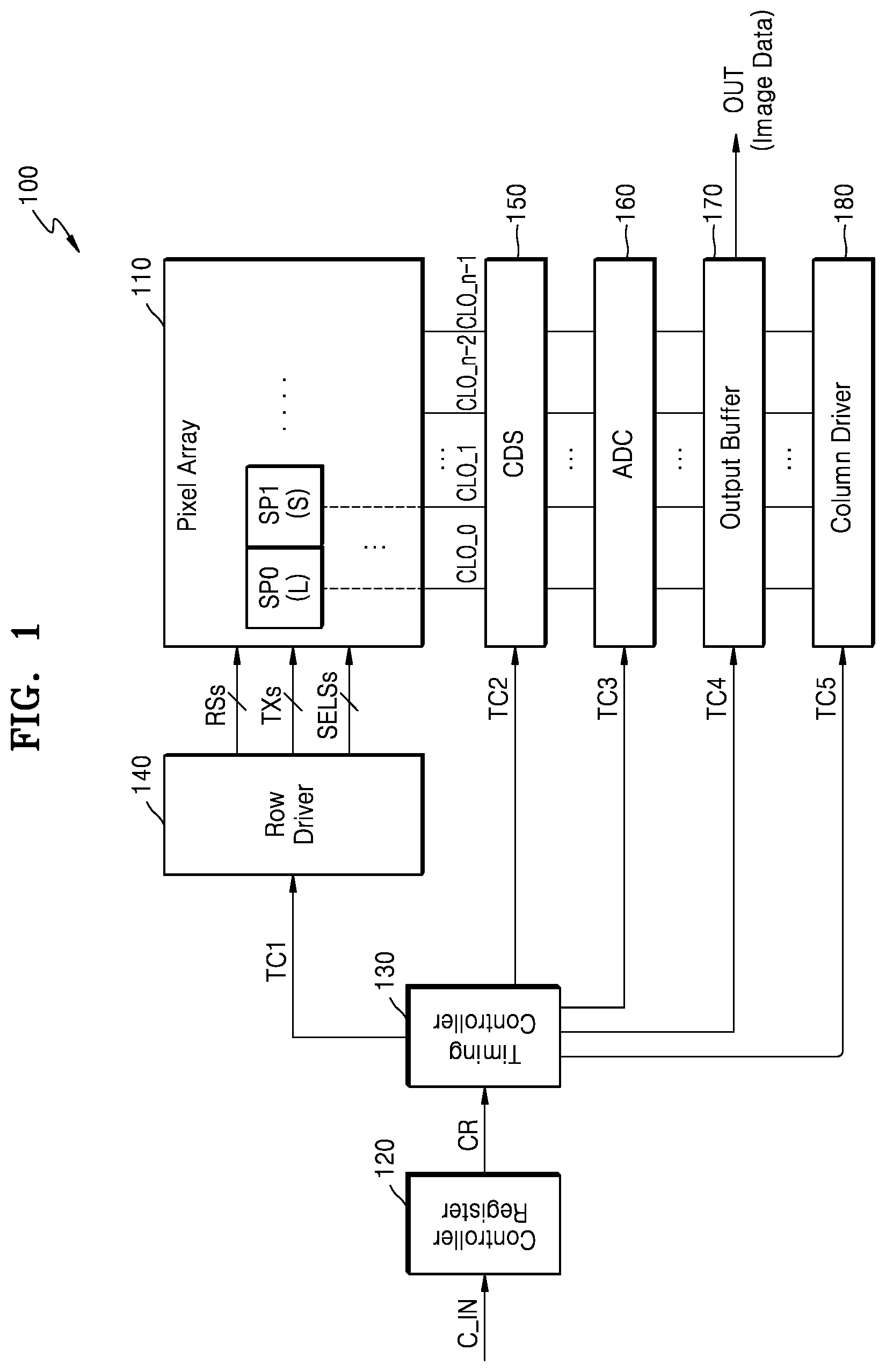
Referring to , an image sensor 100 may include a pixel array 110 , a control register 120 , a timing controller 130 , a row driver 140 , a correlated-double sampling (hereinafter, CDS) 150 , an analog-digital converter (hereinafter, ADC) 160 , an output buffer 170 , and a column driver 180 . The pixel array 110 may include a plurality of shared pixels arranged in rows and columns. The plurality of shared pixels may include a first shared pixel SP 0 and a second shared pixel SP 1 . Each of the shared pixels may include a plurality of sub-pixels. The second shared pixel SP 1 may be disposed adjacent to the first shared pixel SP 0 in a row direction.
The first shared pixel SP 0 may include two or more photo diodes exposed to light for a long time to generate a predetermined pixel signal and a first floating diffusion region in which photo diodes of the first shared pixel SP 0 are shared, and the second shared pixel SP 1 may include two or more photo diodes exposed to light for a short time to generate a predetermined pixel signal and a second floating diffusion region in which photo diodes of the second shared pixel SP 1 are shared. Hereinafter, the term “long time” may be referred to a period of time longer than that of “short time.” For example, a period of time of “long time” may be a period of time of “short time” by n times, n is a positive integer greater than 1. The exposure to light may be based on a timing for accumulating photocharge for each pixel or sub-pixel. As an example, when an image corresponding to a frame is captured, an amount of photocharge accumulated in each of photo diodes of the first shared pixel SP 0 may be greater than an amount of photocharge accumulated in each of photo diodes of the second shared pixel SP 1 . In addition, spectral sensitivities of the first shared pixel SP 0 and the second shared pixel SP 1 may differ. For example, the first shared pixel SP 0 may sense a blue color, and the second shared pixel SP 1 may sense a green color. A configuration of the first shared pixel SP 0 or the second shared pixel SP 1 may apply to shared pixels included in the pixel array 110 .
Each of the shared pixels of the pixel array 110 may output a pixel signal to the CDS 150 though first to n−1th column output line CLO_ 0 to CLO_n−1. For example, the first shared pixel SP 0 may be connected to the first column output line CLO_ 0 and then provide a pixel signal to the CDS 150 through the first column output line CLO_ 0 . The second shared pixel SP 1 may be connected to the second column output line CLO_ 1 and then provide a pixel signal to the CDS 150 the second column output line CLO_ 1 .
The image sensor 100 may receive a control input signal C_IN, and generate a data output signal OUT by detecting light through the pixel array 110 . The image sensor 100 may support various operation modes. The image sensor 100 may support a low-resolution operation mode, a high-resolution operation mode, and the like. For example, the image sensor 100 may be set as a low-resolution operation mode in a low illumination condition in which an exterior illumination condition is equal to or less than a threshold or in response to an external command, and may generate the data output signal OUT based on the low-resolution operation mode. As an embodiment, when the image sensor 100 is in the low-resolution operation mode, photo diodes of the first shared pixel SP 0 may start to accumulate photocharge at a first time, and photo diodes of the second shared pixel SP 1 may start to accumulate photocharge at a second time. Next, the photocharge accumulated in the first shared pixel SP 0 and photocharge accumulated in the second shared pixel SP 1 may be respectively delivered to the first floating diffusion region and the second floating diffusion region at a third time. Then, in a predetermined read period, a first pixel signal generated in the first shared pixel SP 0 may be output through the first column output line CLO_ 0 , and a second pixel signal generated in the second shared pixel SP 1 may be output through the second column output line CLO_ 1 .
As described above, in the low-resolution operation mode, as the image sensor 100 generates a pixel signal for each unit of shared pixels, the image sensor 100 may operate to secure a wide dynamic range according to a low illumination condition. Hereinafter, a photo diode of a shared pixel accumulating photocharge refers to a sub-pixel of a shared pixel accumulating photocharge.
The image sensor 100 may be set as a high-resolution operation mode in a high illumination condition in which an exterior illumination condition is equal to or greater than a threshold or in response to an external command, and may generate the data output signal OUT based on the high-resolution operation mode. Hereinafter, to describe the high-resolution operation mode of the image sensor 100 , it is assumed that the first shared pixel SP 0 includes a first photo diode corresponding to a first sub-pixel and a second photo diode corresponding to a second sub-pixel, and the second shared pixel SP 1 includes a third photo diode corresponding to a third sub-pixel and a fourth photo diode corresponding to a fourth sub-pixel. As an embodiment, when the image sensor 100 is in the high-resolution operation mode, for the first photo diode and the second photo diode of the first shared pixel SP 0 , each timing of starting to accumulate photocharge may differ, and for the third photo diode and the fourth photo diode of the second shared pixel SP 1 , each timing of starting to accumulate photocharge may differ. Then, photocharge accumulated in the first photo diode and photocharge accumulated in the third photo diode may be respectively delivered to the first floating diffusion region and the second floating diffusion region at the same time, and photocharge accumulated in the second photo diode and photocharge accumulated in the fourth photo diode may be respectively delivered to the first floating diffusion region and the second floating diffusion region at the same time. Then, in a first read period, a pixel signal corresponding to photocharge accumulated in the first photo diode may be output through the first column output line CLO_ 0 connected to the first shared pixel SP 0 , and a pixel signal corresponding to photocharge accumulated in the third photo diode may be output through the second column output line CLO_ 1 connected to the second shared pixel SP 1 . In a second read period, a pixel signal corresponding to photocharge accumulated in the second photo diode may be output through the first column output line CLO_ 0 connected to the first shared pixel SP 0 , and a pixel signal corresponding to photocharge accumulated in the fourth photo diode may be output through the second column output line CLO_ 1 connected to the second shared pixel SP 1 .
As described above, in the high-resolution operation mode, the image sensor 100 may generate a pixel signal as a sub-pixel unit constituting a shared pixel and thus, may operate to secure a wide dynamic range according to a high illumination condition.
The control register 120 may include a plurality of registers storing values according to the control input signal C_IN. For example, the control input signal C_IN may include information on an operation mode of the image sensor 100 , and the control register 120 may include a register storing a value indicating an operation mode of the image sensor 100 . The control register 120 may provide a control register signal CR including values stored in the control register 120 to the timing controller 130 . Although not illustrated in , the control register 120 may provide a separate control register signal to each of the row driver 140 and the column driver 180 .
The timing controller 130 may control an operation timing of the image sensor 100 . The timing controller 130 may control an operation timing of the image sensor 100 based on the control register signal CR received from the control register 120 . As an example, the timing controller 130 may set a time needed to finish a read for output signals output from shared pixels included in the pixel array 110 depending on an operation mode such as the low-resolution operation mode and the high-resolution operation mode, and generate first to fifth timing signals TC 1 to TC 5 according to the set time. The timing controller 130 may provide the first to fifth timing signals TC 1 to TC 5 to the row driver 140 , the CDS 150 , the ADC 160 , the output buffer 170 , and the column driver 180 . Each of the row driver 140 , the CDS 150 , the ADC 160 , the output buffer 170 , and the column driver 180 may operate in response to the received first to fifth timing signals TC 1 to TC 5 . For example, the timing controller 130 may control an operation of generating a pixel signal from the pixel array 110 based on various operation modes. However, the control operation of the timing controller 130 described with reference to is an example and is not limited thereto. The control operation may have various embodiments.
The row driver 140 may generate reset control signals, transmission control signals, and selection signals RSs, TXs, and SELSs for controlling the pixel array 110 . As illustrated in , the row driver 140 may provide, in response to the first timing signal TC 1 , the reset control signals RSs, the transmission control signals TXs, and the selection signals SELSs to a plurality of pixels included in the pixel array 110 . The row driver 140 may determine activation and deactivation timings of the reset control signals RSs, the transmission control signals TXs, the selection signals SELSs based on various operation modes (e.g., the low-resolution operation mode or the high-resolution operation mode).
The CDS 150 may sequentially perform sampling and holding of a reference signal and a pixel signal provided from each of the first to n−1th column output lines CLO_ 0 to CLO_n−1 from the pixel array 110 . The CDS 150 may transmit, in response to the second timing signal TC 2 , a reference signal and a pixel signal of each of the first to n−1th column output lines CLO_ 0 to CLO_n−1 as a correlated-double sampling signal to the ADC 160 . The ADC 160 may convert a correlated-double sampling signal of each of the first to n−1th column output lines CLO_ 0 to CLO_n−1, output from the CDS 150 , into a digital signal to output to the output buffer 170 in response to the third timing signal TC 3 . The output buffer 170 may capture and output image data of each column output line, provided from the ADC 160 , in response to the fourth timing signal TC 4 . The output buffer 170 may operate as an interface for compensating a difference in transmission speeds between the image sensor 100 and another device connected to the image sensor 100 . The column driver 180 may select a column output line of the output buffer 170 in response to the fifth timing signal TC 5 , and generate control signals to output the data output signal OUT including image data corresponding to the selected column output line from the output buffer 170 .
illustrates a view showing an embodiment of a pixel array of according to example embodiments.
Referring to , a pixel array 210 a may include a plurality of pixels disposed along a plurality of rows and columns. For example, a shared pixel defined as a unit including pixels disposed in two rows adjacent to each other and two columns adjacent to each other may include four sub-pixels (e.g., 2×2 pixels). For example, the shared pixel may include four photo diodes respectively corresponding to four sub-pixels. For example, a first set of pixels (e.g., two sub-pixels) of a first shared pixel may be disposed in a first row and a second set of pixels (e.g., two other sub-pixels) of the first shared pixel may be disposed in a second row adjacent to the first row. So, the first shared pixel is disposed in two rows and two columns. As illustrated in , the pixel array 210 a may include first to sixteenth shared pixels SP 0 to SP 15 . The pixel array 210 a may include a color filter so that the first to sixteenth shared pixels SP 0 to SP 15 may sense various colors. As an example, a color filter may include filters sensing red (R), green (G), and blue (B), and the first to sixteenth shared pixels SP 0 to SP 15 as one unit may include sub-pixels in which the same color filter is disposed. For example, the first shared pixel SP 0 , the third shared pixel SP 2 , the ninth shared pixel SP 8 and the eleventh shared pixel SP 10 may include sub-pixels including a blue (B) color filter, the second shared pixel SP 1 , the fourth shared pixel SP 3 , the fifth shared pixel SP 4 , the seventh shared pixel SP 6 , the tenth shared pixel SP 9 , the twelfth shared pixel SP 11 , the thirteenth shared pixel SP 12 and the fifteenth shared pixel SP 14 may include sub-pixels including a green (G) color filter, and the sixth shared pixel SP 5 , the eighth shared pixel SP 7 , the fourteenth shared pixel SP 13 and the sixteenth shared pixel SP 15 may include sub-pixels including a red (R) color filter. Also, a group including the first shared pixel SP 0 , the second shared pixel SP 1 , the fifth shared pixel SP 4 and the sixth shared pixel SP 5 , a group including the third shared pixel SP 2 , the fourth shared pixel SP 3 , the seventh shared pixel SP 6 and the eighth shared pixel SP 7 , a group including the ninth shared pixel SP 8 , the tenth shared pixel SP 9 , the thirteenth shared pixel SP 12 and the fourteenth shared pixel SP 13 , and a group including the eleventh shared pixel SP 10 , the twelfth shared pixel SP 11 , the fifteenth shared pixel SP 14 and the sixteenth shared pixel SP 15 may be each disposed to correspond to a Bayer pattern in the pixel array 210 a . In example embodiments, the pixel array 201 a may include a first color pattern, for example, B, G, B, and G in a first row, and a second color pattern, for example, G, R, G, and R in a second row adjacent to the first row. The pixel array 201 a may also include a third color pattern, for example, G, B, G, and B in a first column, and a fourth color pattern, for example, R, G, R, and G in a second column adjacent to the first column.
However, the above is an embodiment, and the pixel array 210 a according to different embodiments of the inventive concept may include various types of color filters. For example, a color filter may include filters for sensing yellow, cyan, magenta and green colors. Alternatively, a color filter may include filters for sensing red, green, blue and white colors. In addition, the pixel array 210 a may include more shared pixels than described, and a disposition of each of the first to sixteenth shared pixels SP 0 to SP 15 may be embodied in various ways and the inventive concept is not limited to .
A and 3 B illustrate the shared pixel of according to other example embodiments. A and 3 B illustrate example embodiments in which one shared pixel includes sub-pixels in various numbers.
Referring to A , each of the first, second, fifth, and sixth shared pixels SP 0 , SP 1 , SP 4 , and SP 5 as a unit may include nine sub-pixels. In the same manner as described in , the first shared pixel SP 0 may include nine sub-pixels including a blue (B) color filter, and the second shared pixel SP 1 and the fifth shared pixel SP 4 may each include nine sub-pixels including a green (G) color filter. The sixth shared pixel SP 5 may include nine sub-pixels including a red (R) color filter.
As another example, referring to B , each of the first, second, fifth, and sixth shared pixels SP 0 , SP 1 , SP 4 , and SP 5 as a unit may include sixteen sub-pixels. In the same manner as described in , the first shared pixel SP 0 may include sixteen sub-pixels including a blue (B) color filter, and the second shared pixel SP 1 and the fifth shared pixel SP 4 may each include sixteen sub-pixels including a green (G) color filter. The sixth shared pixel SP 5 may include sixteen sub-pixels including a red (R) color filter.
A and 4 B illustrate views of the pixel array of , including shared pixels disposed according to an exposure time to generate image data with high sensitivity, according to example embodiments.
Referring to A , a pixel array 210 b may include shared pixels exposed for a long time and shared pixels exposed for a short time. The shared pixel exposed for a long time is a shared pixel for generating a pixel signal by being continuously exposed to light (e.g., accumulating photocharge) for a constant exposure period, and the shared pixel exposed for a short time is a shared pixel for generating a pixel signal by being intermittently exposed to light for a constant exposure period. The shared pixel exposed for a long time may include a plurality of photo diodes for being exposed to light (e.g., accumulating photocharge) for a long time, and the shared pixel exposed for a short time may include a plurality of photo diodes for being exposed to light for a short time. Hereinafter, it is assumed that a shared pixel marked with L is the shared pixel exposed for a long time, and a shared pixel marked with S is the shared pixel exposed for a short time. As an embodiment, as illustrated in A , the first shared pixel SP 0 , the third shared pixel SP 2 , the fourth shared pixel SP 3 , the seventh shared pixel SP 6 , the ninth to eleventh shared pixels SP 8 to SP 10 , and the thirteenth shared pixel SP 12 may be the shared pixels exposed for a long time, and other shared pixels SP 1 , SP 4 , SP 5 , SP 7 , SP 11 , and SP 13 to SP 15 may be the shared pixels exposed for a short time.
B illustrates, unlike A , a view of an embodiment in which the shared pixel exposed for a long time and the shared pixel exposed for a short time are disposed. As illustrated in B , a pixel array 210 c may include shared pixels exposed for a long time and shared pixels exposed for a short time. In addition, the first to third shared pixels SP 0 to SP 2 , the seventh shared pixel SP 6 , the ninth shared pixel SP 8 , the eleventh shared pixel SP 10 , the twelfth shared pixel SP 11 , and the thirteenth shared pixel SP 12 may be the shared pixels exposed for a long time, and the other shared pixels SP 3 , SP 4 , SP 5 , SP 7 , SP 9 , and SP 13 to SP 15 may be the shared pixels exposed for a short time. However, the pixel arrays 210 b and 210 c illustrated in A and 4 B are example embodiments, and thus, the inventive concept is not limited thereto. A pixel array in which the shared pixel exposed for a long time and the shared pixel exposed for a short time are disposed by utilizing one or more disposition methods may be embodied. Furthermore, in the imaging within one frame, the pixel arrays 210 b and 210 c may perform the imaging by using a spatially varying exposure (SVE) method in which an exposure period is regularly changed in one frame and may be embodied to have a wide dynamic range effect by using a signal procession technology.
A and 5 B illustrate views showing an image sensor according to example embodiments of the inventive concept. In A and 5 B , a blue sub-pixel and a green sub-pixel are illustrated as an example from among a plurality of sub-pixels included in an image sensor. In addition, although as shared pixels including 2×2 sub-pixels are illustrated, and A and 5 B illustrate cross-sectional views of some portions of image sensors, and thus two sub-pixels for a shared pixel are illustrated.
As illustrated in A and 5 B , image sensors 300 a and 300 b may include a plurality of photo diodes 310 , a plurality of blue and green color filters 320 , and a plurality of micro lenses 330 a and 330 b . In addition, although not illustrated in A and 5 B , a floating diffusion region (not shown) receiving photocharge from the photo diodes 310 may be formed in a substrate in which the photo diodes 310 are disposed.
As an embodiment, a shared pixel may include four sub-pixels. Although only two sub-pixels corresponding to a shared pixel are illustrated in A and 5 B , the first shared pixel SP 0 may substantially include four sub-pixels generating a pixel signal with high sensitivity. The first shared pixel SP 0 may include the blue (B) color filters 320 as illustrated in or the like. For example, the first shared pixel SP 0 may include photo diodes PD(L) corresponding to sub-pixels. The second sub-pixel SP 1 may include four sub-pixels generating a pixel signal with low sensitivity. The second shared pixel SP 1 may include the green (G) color filters 320 as illustrated in or the like. For example, the second shared pixel SP 1 may include photo diodes PD(S) corresponding to sub-pixels.
As illustrated in A , each of the micro lenses 330 a may be disposed to correspond to the first and second shared pixels SP 0 and SP 1 . For example, as a micro lens is disposed to correspond to a plurality of sub-pixels, information on a phase-difference between sub-pixels is generated to obtain information on depth, and thus, an auto focusing function may be performed.
As another embodiment, as illustrated in B , the image sensor 300 b may include micro lenses 330 b disposed to respectively correspond to a plurality of sub-pixels. In addition, sizes of a long-time exposed photo diode PD(L) of the first shared pixel SP 0 and a short-time exposed photo diode PD(S) of the second shared pixel SP 1 may be the same, and thus, a process of manufacturing the micro lenses 330 b disposed to respectively correspond to the sub-pixels may be relatively easy. Furthermore, when the sizes of the micro lenses are different from each other, a pixel having a lens of a big size may affect a pixel having a lens of a small size thereby causing a shading, but the inventive concept may reduce the likelihood of the occurrence of a shading.
illustrates a view showing a connection between a row driver and a pixel array of in detail, according to example embodiments.
Referring to , a pixel array 410 may include first to sixteenth shared pixels SP 0 to SP 15 . In the pixel array 410 , a shared pixel exposed for a long time L and a shared pixel exposed for a short time S may be disposed according to the embodiment described with reference to A. The first to sixteenth shared pixels SP 0 to SP 15 may each include four sub-pixels SubP 00 to SubP 153 . Hereinafter, as an embodiment, a shared pixel including 2×2 sub-pixels will be mainly described as illustrated in .
The pixel array 410 may be connected to the row driver 440 through transmission control signal lines TG 0 to TG 31 , reset signal lines RG 0 to RG 3 , and selection signal lines SEL 0 to SEL 3 . The first to fourth shared pixels SP 0 to SP 3 may share the first reset signal line RG 0 and the first selection signal line SEL 0 , the fifth to eighth shared pixel SP 4 to SP 7 may be connected to the second reset signal line RG 1 and the second selection signal line SEL 1 , the ninth to twelfth shared pixels SP 8 to SP 11 may be connected the third reset signal line RG 2 and the third selection signal line SEL 2 , and the thirteenth to sixteenth shared pixels SP 12 to SP 15 may be connected to the fourth reset signal line RG 3 and the fourth selection signal line SEL 3 . Row lines Row 0 to Row 7 may respectively include four transmission control signal lines TG 0 to TG 3 , TG 4 to TG 7 , TG 8 to TG 11 , TG 12 to TG 15 , TG 16 to TG 19 , TG 20 to TG 23 , TG 24 to TG 27 , and TG 28 to TG 31 . As an example, the first to fourth shared pixels SP 0 to SP 3 may be connected to the first and second row lines Row 0 and Row 1 , the first reset signal line RG 0 , and the first selection signal line SEL 0 .
In example embodiments, a first set of pixels (e.g., two sub-pixels) of each of the first to fourth shared pixels SP 0 to SP 3 may correspond to the four transmission control signal lines TG 0 to TG 3 of the first row line Row 0 , and a second set of pixels (e.g., other two sub-pixels) of each of the first to fourth shared pixels SP 0 to SP 3 may correspond to the four transmission control signal lines TG 4 to TG 7 of the second row line Row 1 .
The row lines Row 0 to Row 7 may respectively include the transmission control signal lines TG 0 and TG 1 , TG 4 and TG 5 , TG 8 and TG 9 , TG 12 and TG 13 , TG 16 and TG 17 , TG 20 and TG 21 , TG 24 and TG 25 , and TG 28 and TG 29 for providing a control signal for a short-time exposure to light, and may also respectively include the transmission control signal lines TG 2 and TG 3 , TG 6 and TG 7 , TG 10 and TG 11 , TG 14 and TG 15 , TG 18 and TG 19 , TG 22 and TG 23 , TG 26 and TG 27 , and TG 30 and TG 31 for providing a control signal of a long-time exposure to light. For example, the first row line Row 0 may include the first and second transmission control signal lines TG 0 and TG 1 for providing a control signal of a short-time exposure to light, and the third and fourth transmission control signal lines TG 2 and TG 3 for providing a control signal of a long-time exposure to light.
The first shared pixel SP 0 may include sub-pixels SubP 00 to SubP 03 each including a photo diode for a long-time exposure to light as the shared pixel exposed for a long time L. For a long-time exposure control, the sub-pixel SubP 00 may be connected to the fourth transmission control signal line TG 3 , the sub-pixel SubP 01 may be connected to the third transmission control signal line TG 2 , the sub-pixel SubP 02 may be connected to the eighth transmission control signal line TG 7 , and the sub-pixel SubP 03 may be connected to the seventh transmission control signal line TG 6 . The second shared pixel SP 1 may include sub-pixels SubP 10 to SubP 13 each including a photo diode for a short-time exposure to light as the shared pixel exposed for a short time S. For controlling a short-time exposure to light, the sub-pixel SubP 10 may be connected to the second transmission control signal line TG 1 , the sub-pixel SubP 11 may be connected to the first transmission control signal line TG 0 , the sub-pixel SubP 12 may be connected to the sixth transmission control signal line TG 5 , and the sub-pixel SubP 13 may be connected to the fifth transmission control signal line TG 4 . A configuration of the first shared pixel SP 0 or the second shared pixel SP 1 as described above may be applied to other third to sixteenth shared pixels SP 2 to SP 15 .
Taking into account the configuration of the pixel array 410 and the row driver 440 above, an operation for generating image data based on the high-resolution operation mode or the low-resolution operation mode may be flexibly performed. However, the configuration illustrated in is an example embodiment, and the inventive concept is not limited thereto. Various configurations that allow a specific operation of an image sensor described below to be performed may be used.
illustrates a circuit diagram corresponding to some shared pixels of the pixel array of according to example embodiments. illustrates a circuit diagram showing the first to eighth shared pixels SP 0 to SP 7 connected to the first to sixteenth transmission control signal lines TG 0 to TG 15 . Referring to , a first pixel circuit PC 0 to an eighth pixel circuit PC 7 may respectively correspond to the first shared pixel SP 0 to the eighth shared pixel SP 7 of . The first pixel circuit PC 0 may include one or more photo diodes G 00 to G 03 exposed to light for a long time and sensing a green (G) color. The first pixel circuit PC 0 may include the transmission transistors TR 00 to TR 03 for controlling a transmission of photocharge accumulated in the photo diodes G 00 to G 03 . The transmission transistor TR 00 may be connected to the fourth transmission control signal line TG 3 , the transmission transistor TR 01 may be connected to the third transmission control signal line TG 2 , the transmission transistor TR 02 may be connected to the eighth transmission control signal line TG 7 , and the transmission transistor TR 03 may be connected to the seventh transmission control signal line TG 6 . Through the aforementioned connection, a long-time exposure control for the first pixel circuit PC 0 , based on the transmission control signals controlling accumulated photocharge may be possible. However, this is merely an example embodiment, and thus, the inventive concept is not limited thereto. The photo diodes of the first pixel circuit PC 0 and the transmission transistors may be disposed in various numbers. In addition, the first pixel circuit PC 0 may further include a first floating diffusion region FD 0 , a first driving transistor TD 0 , a first reset transistor TRT 0 and a first selection transistor TS 0 . The photo diodes G 00 to G 03 may share the first floating diffusion region FD 0 .
A second pixel circuit PC 1 may include one or more photo diodes R 10 to R 13 exposed to light for a short time and sensing red (R) color. The second pixel circuit PC 1 may include the transmission transistors TR 10 to TR 13 for controlling a transmission of photocharge accumulated in the photo diodes R 10 to R 13 . The transmission transistor TR 10 may be connected to the second transmission control signal line TG 1 , transmission transistor TR 11 may be connected to the first transmission control signal line TG 0 , transmission transistor TR 12 may be connected to the sixth transmission control signal line TG 5 , and transmission transistor TR 13 may be connected to the fifth transmission control signal line TG 4 . Through the aforementioned connection, a control for the second pixel circuit PC 1 to be exposed to light for a short time, based on the transmission control signals controlling accumulated photocharge may be possible. In addition, the second pixel circuit PC 1 may further include a second floating diffusion region FD 1 , a second driving transistor TD 1 , a second reset transistor TRT 1 , and a second selection transistor TS 1 . The photo diodes R 10 to R 13 may share the second floating diffusion region FD 1 .
A configuration of the first pixel circuit PC 0 or the second pixel circuit PC 1 is applied to the third to eighth pixel circuits PC 2 to PC 7 , and thus, detailed descriptions thereof will be omitted.
The first pixel circuit PC 0 and the fifth pixel circuit PC 4 may be connected to the first column output line CLO_ 0 , the second pixel circuit PC 1 and the sixth pixel circuit PC 5 may be connected to the second column output line CLO_ 1 , the third pixel circuit PC 2 and the seventh pixel circuit PC 6 may be connected to the third column output line CLO 2 , and the fourth pixel circuit PC 3 and the eighth pixel circuit PC 7 may be connected to the fourth column output line CLO_ 3 . Hereinafter, a detailed control operation of a timing controller for the pixel circuits above will be described.
A and 8 B illustrate views showing a control method of a timing controller for a pixel circuit generating a pixel signal in the low-resolution operation mode, according to example embodiments.
Referring to A , the third transmission control signal TX 2 , the fourth transmission control signal TX 3 , the seventh transmission control signal TX 6 , and the eighth transmission control signal TX 7 may have waveforms corresponding to the photo diodes G 00 to G 03 included in the first pixel circuit PC 0 , photo diodes G 20 to G 23 included in the third pixel circuit PC 2 , and photo diodes R 30 to R 33 included in the fourth pixel circuit PC 3 to accumulate photocharge during a first period of time T 1 (e.g., a long time) which is relatively long. For example, in the low-resolution operation mode, by using the third, fourth, seventh, and eighth transmission control signals TX 2 , TX 3 , TX 6 , and TX 7 , the first pixel circuit PC 0 , the third pixel circuit PC 2 and the fourth pixel circuit PC 3 that require a long-time exposure control may be controlled such that an exposure to light may start at the same first time.
The first transmission control signal TX 0 , the second transmission control signal TX 1 , the fifth transmission control signal TX 4 , and the sixth transmission control signal TX 5 may have waveforms corresponding to the photo diodes R 10 to R 13 included in the second pixel circuit PC 1 to accumulate photocharge during a second period of time T 2 (e.g., a short time), which is relatively short. For example, the first, second, fifth, and sixth transmission control signals TX 0 , TX 1 , TX 4 , and TX 5 may control the second pixel circuit PC 1 that requires a short-time exposure control to start exposure to light at a second timing.
After an exposure to light is completed for a preset time for the photo diodes G 00 to G 03 , R 10 to R 13 , G 20 to G 23 , and R 30 to R 33 respectively included in the first pixel circuit PC 0 , the second pixel circuit PC 1 , the third pixel circuit PC 2 , and the fourth pixel circuit PC 3 , an operation of outputting a pixel signal depending on photocharge accumulated in the photo diodes G 00 to G 03 , R 10 to R 13 , G 20 to G 23 , and R 30 to R 33 may be performed. In detail, the first to eighth transmission control signals TX 0 to TX 7 may have a logic high value for a predetermined period (e.g. a first transmission period T a ) so that photocharge accumulated in the photo diodes G 00 to G 03 , R 10 to R 13 , G 20 to G 23 , and R 30 to R 33 may be respectively delivered to the floating diffusion regions FD 0 to FD 3 . Also, for a period including the first transmission period T a (e.g., read period, ITV a1 ), a first reset control signal RS 0 may have a logic low value so that each of the reset transistors TRT 0 to TRT 3 is turned off. In addition, a first selection signal SELS 0 may have a logic high value for the read period ITV a1 so that a reference signal and a pixel signal are output from the first to fourth pixel circuits PC 0 to PC 3 for the read period ITV a1 .
In detail, for the read period ITV a1 , a reference signal and a pixel signal may be output, the reference signal corresponding to an electric potential of each of the floating diffusion regions FD 0 to FD 3 reset to a predetermined power supply voltage level VDD according to a reset operation, and the pixel signal corresponding to an electric potential of each of the floating diffusion regions FD 0 to FD 3 , after each photocharge accumulated in the photo diodes G 00 to G 03 , R 10 to R 13 , G 20 to G 23 , and R 30 to R 33 is respectively delivered to the floating diffusion regions FD 0 to FD 3 .
Meanwhile, further referring to B , a plurality of photo diodes included in a pixel circuit may have a structure in which a driving transistor, a reset transistor, and a selection transistor are shared. In the low-resolution operation mode, transmission control signals having the same pattern may be applied to transmission transistors included in a pixel circuit corresponding to the shared pixel exposed for a long time, and transmission control signals having the same pattern may be applied to transmission transistors included in a pixel circuit corresponding to the shared pixel exposed for a short time. For example, in the low-resolution operation mode, the transmission transistors TR 00 to TR 03 of the first pixel circuit PC 0 , the transmission transistors TR 20 to TR 23 of the third pixel circuit PC 2 , and the transmission transistors TR 30 to TR 33 of the fourth pixel circuit PC 3 , may respectively receive the third transmission control signal TX 2 , the fourth transmission control signal TX 3 , the seventh transmission control signal TX 6 , and the eighth transmission control signal TX 7 , each having a first signal pattern and thus, a long-time exposure may be controlled for each photo diode of the first, third, and fourth pixel circuits PC 0 , PC 2 , and PC 3 . Also, in the low-resolution operation mode, the transmission transistors TR 10 to TR 13 of the second pixel circuit PC 1 may respectively receive the first transmission control signal TX 0 , the second transmission control signal TX 1 , the fifth transmission control signal TX 4 , and the sixth transmission control signal TX 5 , each having a second signal pattern and thus, a short-time exposure may be controlled for each photo diode of the second pixel circuit PC 1 .
In response to the first selection signal SELS 0 having a logic high value for the read period ITV a1 in the low-resolution operation mode, the pixel circuits PC 0 to PC 3 may output a pixel signal as respective multi-row lines unit through the first to fourth column output lines CLO_ 0 to CLO_ 3 respectively connected thereto. For example, the first pixel circuit PC 0 may generate, in response to the first selection signal SELS 0 , a pixel signal Psig_a 0 by using photocharge accumulated in photo diodes G 00 and G 01 connected to the transmission control signal lines TG 3 and TG 2 corresponding to the first row line Row 0 and in the photo diode G 02 and G 03 connected to the transmission control signal lines TG 7 and TG 6 corresponding to the second row line Row 1 . The first pixel circuit PC 0 may output the pixel signal Psig_a 0 through the first column output line CLO_ 0 . As described above, in the low-resolution operation mode, the pixel circuits PC 0 to PC 3 according to the inventive concept may respectively generate pixel signals Psig_a 0 to Psig_a 3 for a multi row lines unit by using the photo diodes connected to the first row line Row 0 and the second row line Row 1 . However, this is an example embodiment, and the inventive concept is not limited thereto. As illustrated in A and 4 B , when the shared pixel includes nine or sixteen sub-pixels, an image sensor may be embodied so as to generate a pixel signal in a unit of three or more row lines.
In example embodiments, in the low-resolution operation mode, each photocharge accumulated in the photo diodes G 00 to G 03 , R 10 to R 13 , G 20 to G 23 , and R 30 to R 33 may be simultaneously delivered to a corresponding floating diffusion region of the floating diffusion regions FD 0 to FD 3 and then each reference signal and each pixel signal of the floating diffusion regions FD 0 to FD 3 may be simultaneously output.
According to example embodiments, in the low-resolution operation mode, light detection is controlled by using a plurality of photo diodes included in the shared pixel so as to generate a pixel signal and thus, a wide dynamic range may be secured even under the low illumination condition.
A and 9 B illustrate views showing a control method of a timing controller for a pixel circuit generating a pixel signal in the low-resolution operation mode, according to example embodiments.
A and 8 B are illustrated to describe a control method used when the first to fourth pixel circuits PC 0 to PC 3 are selected in response to the first selection signal SELS 0 , and A and 9 B are illustrated to describe a control method used when the fifth to eighth pixel circuits PC 4 to PC 7 are selected in response to a second selection signal SELS 1 after the first to fourth pixel circuits PC 0 to PC 3 are selected in response to the first selection signal SELS 0 and generate pixel signals.
Referring to A , the eleventh transmission control signal TX 10 , the twelfth transmission control signal TX 11 , the fifteenth transmission control signal TX 14 and the sixteenth transmission control signal TX 15 may have a waveform corresponding to the photo diodes B 60 to B 63 included in the seventh pixel circuit PC 6 to accumulate photocharge during a first period of time T 1 (e.g., a long time), which is relatively long. For example, by using the eleventh, twelfth, fifteenth, and sixteenth transmission control signals TX 10 , TX 11 , TX 14 , and TX 15 , the seventh pixel circuit PC 6 that requires a long-time exposure control may be controlled to start exposure to light at a first time.
The ninth transmission control signal TX 8 , the tenth transmission control signal TX 9 , the thirteenth transmission control signal TX 12 , and the fourteenth transmission control signal TX 13 may have a waveform corresponding to the photo diodes B 40 to B 43 included in the fifth pixel circuit PC 4 , the photo diodes G 50 to G 53 included in the sixth pixel circuit PC 5 , and the photo diodes G 70 to G 73 included in the eighth pixel circuit PC 7 to accumulate photocharge during a second period of time T 2 (e.g., a short time), which is relatively short. For example, by using the ninth, tenth, thirteenth, and fourteenth transmission control signals TX 8 , TX 9 , TX 12 , and TX 13 , the fifth pixel circuit PC 4 , the sixth pixel circuit PC 5 , and the eighth pixel circuit PC 7 that require a short-time exposure control may be controlled to start exposure to light at the same second timing.
After an exposure to light is completed for a preset time for the photo diodes B 40 to B 43 , G 50 to G 53 , B 60 to B 63 , and G 70 to G 73 respectively included in the fifth pixel circuit PC 4 , the sixth pixel circuit PC 5 , the seventh pixel circuit PC 6 , and the eighth pixel circuit PC 7 , an operation outputting a pixel signal may be performed depending on photocharge accumulated in the photo diodes B 40 to B 43 , G 50 to G 53 , B 60 to B 63 , and G 70 to G 73 . In detail, the ninth to sixteenth transmission control signals TX 8 to TX 15 may have a logic high value for a predetermined period (e.g., the second transmission period, T b ) so that photocharge accumulated in the photo diodes B 40 to B 43 , G 50 to G 53 , B 60 to B 63 , and G 70 to G 73 are respectively delivered to the floating diffusion regions FD 4 to FD 7 . In addition, for a period including the second transmission period T b (e.g., read period, ITV a2 ), a second reset control signal RS 1 may have a logic low value so that each of the reset transistors TRT 4 to TRT 7 is turned off. Also, the second selection signal SELS 1 may have a logic high value for the read period ITV a2 so that a reference signal and a pixel signal may be output from the fifth to eighth pixel circuits PC 4 to PC 7 for the read period ITV a2 .
Particularly, for the read period (ITV a2 ), a reference signal corresponding to an electric potential of each of the floating diffusion regions FD 4 to FD 7 reset to the predetermined power supply voltage level VDD according to a reset operation and respective pixel signals corresponding to an electric potential of each of the floating diffusion regions FD 4 to FD 7 , after each photocharge accumulated in the photo diodes B 40 to B 43 , G 50 to G 53 , B 60 to B 63 , and G 70 to G 73 is respectively delivered to the floating diffusion regions FD 4 to FD 7 , may be output.
Further referring to B , in response to the second selection signal SELS 1 having a logic high value for the read period ITV a2 in the low-resolution operation mode, the pixel circuits PC 4 to PC 7 may output pixel signals as respective multi row lines unit through the column output lines CLO_ 0 to CLO_ 3 respectively connected thereto. For example, the fifth pixel circuit PC 4 , in response to the second selection signal SELS 1 , may generate a pixel signal Psig_b 0 by using photocharge accumulated in the photo diodes B 40 and B 41 connected to the transmission control signal lines TG 9 and TG 8 corresponding to the third row line Row 2 and the photo diodes B 42 and B 43 connected to the transmission control signal lines TG 13 and TG 12 corresponding to the fourth row line Row 3 . The fifth pixel circuit PC 4 may output the pixel signal Psig_b 0 through the first column output line CLO_ 0 . For example, in the low-resolution operation mode, the fifth to eighth pixel circuits PC 4 to PC 7 according to the inventive concept may generate the pixel signals Psig_b 0 to Psig_b 3 as each multi row lines unit by using the photo diodes connected to the third row line Row 2 and the fourth row line Row 3 .
In example embodiments, in the low-resolution operation mode, each photocharge accumulated in the photo diodes B 40 to B 43 , G 50 to G 53 , B 60 to B 63 , and G 70 to G 73 may be simultaneously delivered to a corresponding floating diffusion region of the floating diffusion regions FD 4 to FD 7 and then each reference signal and each pixel signal of the floating diffusion regions FD 4 to FD 7 may be simultaneously output.
A and 10 B illustrate views showing a control method of a timing controller for a pixel circuit generating a pixel signal in the high-resolution operation mode, according to example embodiments.
Referring to A , in the high-resolution operation mode, the fourth transmission control signal TX 3 , the third transmission control signal TX 2 , the eighth transmission control signal TX 7 , and the seventh transmission control signal TX 6 may have a waveform so as to accumulate photocharge during a first period of time T 1 (e.g., a long time), which is relatively long, by staring to accumulate photocharge in an order of a photo diode G 00 , a photo diode G 01 , a photo diode G 02 , and a photo diode G 03 of the first pixel circuit PC 0 , in an order of a photo diode G 20 , a photo diode G 21 , a photo diode G 22 , and a photo diode G 23 of the third pixel circuit PC 2 , and in an order of a photo diode R 30 , a photo diode R 31 , a photo diode R 32 , and a photo diode R 33 of the fourth pixel circuit PC 3 .
In addition, the second transmission control signal TX 1 , the first transmission control signal TX 0 , the sixth transmission control signal TX 5 , and the fifth transmission control signal TX 4 may have a waveform to accumulate photocharge during a second period of time T 2 (e.g., a short time), which is relatively short, by starting to accumulate photocharge in an order of a photo diode R 10 , a photo diode R 11 , a photo diode R 12 , and a photo diode R 13 of the second pixel circuit PC 1 . For example, in the high-resolution operation mode, a timing to start to accumulate photocharge for each photo diode included in the pixel circuits PC 0 to PC 3 may differ. For example, the photo diode G 00 , the photo diode G 01 , the photo diode G 02 , and the photo diode G 03 of the first pixel circuit PC 0 may start to accumulate photocharge at different times.
After an exposure to light is completed for a preset time for the photo diodes G 00 to G 03 , R 10 to R 13 , G 20 to G 23 , and R 30 to R 33 respectively included in the first pixel circuit PC 0 , the second pixel circuit PC 1 , the third pixel circuit PC 2 and the fourth pixel circuit PC 3 , an operation of sequentially outputting pixel signals may be performed depending on the photocharge accumulated in the photo diodes G 00 to G 03 , R 10 to R 13 , G 20 to G 23 , and R 30 to R 33 .
The fourth transmission control signal TX 3 and the second transmission control signal TX 1 may have a logic high value for a first transmission period T 11 so that the photocharge accumulated in the photo diode G 00 of the first pixel circuit PC 0 , the photo diode R 10 of the second pixel circuit PC 1 , the photo diode G 20 of the third pixel circuit PC 2 , and the photo diode R 30 of the fourth pixel circuit PC 3 are delivered to respective floating diffusion regions FD 0 to FD 3 .
The first reset control signal RS 0 may have a low value so that each of the reset transistors TRT 0 to TRT 3 is turned off for a first read period ITV b11 including the first transmission period T 11 . In addition, the first selection signal SELS 0 may have a logic high value for the first read period ITV b11 so that a reference signal and a pixel signal are output from each of the first pixel circuit PC 0 to the fourth pixel circuit PC 3 for the first read period ITV b11 . For the first read period ITV b11 , a reference signal corresponding to an electric potential of each of the floating diffusion regions FD 0 to FD 3 reset to a predetermined power supply voltage level VDD according to a reset operation and a pixel signal corresponding to an electric potential of each of the floating diffusion regions FD 0 to FD 3 , after each photocharge accumulated in the photo diodes GOO, R 10 , G 20 , and R 30 are respectively delivered to the floating diffusion regions FD 0 to FD 3 , may be output.
Also, the third transmission control signal TX 2 and the first transmission control signal TX 0 may have a logic high value for a second transmission period T 12 so that the photocharge accumulated in the photo diode G 01 of the first pixel circuit PC 0 , the photo diode R 11 of the second pixel circuit PC 1 , the photo diode G 21 of the third pixel circuit PC 2 , and the photo diode R 31 of the fourth pixel circuit PC 3 are respectively delivered to the floating diffusion regions FD 0 to FD 3 . The first reset control signal RS 0 may have a low value so that each of the reset transistors TRT 0 to TRT 3 is turned off for a second read period ITV b12 including the second transmission period T 12 . In addition, the first selection signal SELS 0 may have a logic high value for the second read period ITV b12 so that a reference signal and a pixel signal are output from each of the first pixel circuit PC 0 to the fourth pixel circuit PC 3 for the second read period ITV b12 . For the second read period ITV b12 , a reference signal corresponding to an electric potential of each of the floating diffusion regions FD 0 to FD 3 reset to a predetermined power supply voltage level VDD according to a reset operation and a pixel signal corresponding to an electric potential of each of the floating diffusion regions FD 0 to FD 3 , after each photocharge accumulated in the photo diodes G 01 , R 11 , G 21 , and R 31 are respectively delivered to the floating diffusion regions FD 0 to FD 3 , may be output.
In a manner as described above, a reference signal and a pixel signal may be generated for a third read period ITV b13 by using the photo diode G 02 of the first pixel circuit PC 0 , the photo diode R 12 of the second pixel circuit PC 1 , the photo diode G 22 of the third pixel circuit PC 2 , and the photo diode R 32 of the fourth pixel circuit PC 3 , and a reference signal and a pixel signal may be generated for a fourth read period (ITV b14 ) by using the photo diode G 03 of the first pixel circuit PC 0 , the photo diode R 13 of the second pixel circuit PC 1 , the photo diode G 23 of the third pixel circuit PC 2 , and the photo diode R 33 of the fourth pixel circuit PC 3 . Detailed descriptions thereof are omitted.
Meanwhile, further referring to B , a plurality of photo diodes included in a pixel circuit may have a structure in which a driving transistor, a reset transistor, and a selection transistor are shared. In the high-resolution operation mode, transmission control signals with different patterns may be applied to transmission transistors included in a pixel circuit. For example, in the high-resolution operation mode, the transmission transistors TR 00 to TR 03 of the first pixel circuit PC 0 , the transmission transistors TR 20 to TR 23 of the third pixel circuit PC 2 , and the transmission transistors TR 30 to TR 33 of the fourth pixel circuit PC 3 may respectively receive the third transmission control signal TX 2 , the fourth transmission control signal TX 3 , the seventh transmission control signal TX 6 , and the eighth transmission control signal TX 7 having different signal patterns and thus, a long-time exposure may be controlled for each photo diode of the first, third, and fourth pixel circuits PC 0 , PC 2 , and PC 3 . Also, in the high-resolution operation mode, the transmission transistors TR 10 to TR 13 of the second pixel circuit PC 1 may respectively receive the first transmission control signal TX 0 , the second transmission control signal TX 1 , the fifth transmission control signal TX 4 , and the sixth transmission control signal TX 5 having different signal patterns and thus, a short-time exposure may be controlled for each photo diode of the second pixel circuit PC 1 .
In response to the first selection signal SELS 0 having a logic high value for the first read period ITV b11 in the high-resolution operation mode, the pixel circuits PC 0 to PC 3 may each output a pixel signal as a respective single row line unit through the column output lines CLO_ 0 to CLO_ 3 respectively connected thereto. For example, for the first read period ITV b11 , the first pixel circuit PC 0 , the third pixel circuit PC 2 , and the fourth pixel circuit PC 3 may generate respective pixel signals Psig_c 00 , Psig_c 20 , and Psig_c 30 by using the photocharge accumulated in the photo diode G 00 , the photo diode G 20 , and the photo diode R 30 connected to the fourth transmission control signal line TG 3 corresponding to the first row line Row 0 , and the second pixel circuit PC 1 may generate a pixel signal Psig_c 10 by using the photocharge accumulated in the photo diode R 10 connected to the second transmission control signal line TG 1 corresponding to the first row line Row 0 . In this manner as described above, for the second read period ITV b12 , the pixel circuits PC 0 to PC 3 may respectively generate the pixel signals Psig_c 01 , Psig_c 11 , Psig_c 21 , and Psig_c 31 of a single row line unit corresponding to the first row line Row 0 , and for the third read period ITV b13 , the pixel circuits PC 0 to PC 3 may respectively generate the pixel signals Psig_c 02 , Psig_c 12 , Psig_c 22 , and Psig_c 32 of a single row line unit corresponding to the second row line Row 1 , and for the fourth read period ITV b14 , the pixel circuits PC 0 to PC 3 may respectively generate the pixel signals Psig_c 03 , Psig_c 13 , Psig_c 23 , and Psig_c 33 of a single row line unit corresponding to the second row line Row 1 .
As described above, the photo diodes respectively corresponding to the sub-pixels included in the shared pixel may be individually controlled so that a pixel signal may be generated for each sub-pixel included in the shared pixel in the high-resolution operation mode. For example, regardless of a structure of the shared pixel, a wide dynamic range may also be secured at the same time.
A and 11 B illustrate views showing a control method of a timing controller for a pixel circuit generating a pixel signal in the high-resolution operation mode, according to example embodiments.
A and 10 B illustrate views of a control method when the first to fourth pixel circuits PC 0 to PC 3 are selected in response to the first selection signal SELS 0 . Next, A and 11 B illustrate views of a control method of when the fifth to eighth pixel circuits PC 4 to PC 8 are selected in response to the second selection signal SELS 1 after the first to fourth pixel circuits PC 0 to PC 3 are selected to generate pixel signals in response to the first selection signal SELS 0 .
Referring to A , in the high-resolution operation mode, the twelfth transmission control signal TX 11 , the eleventh transmission control signal TX 10 , the sixteenth transmission control signal TX 15 , and the fifteenth transmission control signal TX 14 may have a waveform to accumulate photocharge during the first period of time T 1 , which is relatively long, by starting to accumulate photocharge in an order of the photo diode B 60 , the photo diode B 61 , the photo diode B 62 , and the photo diode B 63 of the seventh pixel circuit PC 6 .
In the high-resolution operation mode, the tenth transmission control signal TX 9 , the ninth transmission control signal TX 8 , the fourteenth transmission control signal TX 13 , and the thirteenth transmission control signal TX 12 may have a waveform to accumulate photocharge during the second period of time T 2 , which is relatively short, by starting to accumulate photocharge in an order of the photo diode B 40 , the photo diode B 41 , the photo diode B 42 , and the photo diode B 43 of the fifth pixel circuit PC 4 , in an order of the photo diode G 50 , the photo diode G 51 , the photo diode G 52 , and the photo diode G 53 of the sixth pixel circuit PC 5 , and in an order of the photo diode G 70 , the photo diode G 71 , the photo diode G 72 , and the photo diode G 73 of the eighth pixel circuit PC 7 .
After an exposure to light is completed for a preset time for the photo diodes B 40 to B 43 , G 50 to G 53 , B 60 to B 63 , and G 70 to G 73 respectively included in the fifth pixel circuit PC 4 , the sixth pixel circuit PC 5 , the seventh pixel circuit PC 6 , and the eighth pixel circuit PC 7 , an operation of sequentially outputting pixel signals depending on the photocharge accumulated in the photo diodes B 40 to B 43 , G 50 to G 53 , B 60 to B 63 , and G 70 to G 73 may be performed.
Meanwhile, further referring to B , in response to the first selection signal SELS 0 having a logic high value for a first read period ITV b21 in the high-resolution operation mode, the fifth to eighth pixel circuits PC 4 -PC 7 may each output a pixel signal as a respective single row line unit through the column output lines CLO_ 0 to CLO_ 3 respectively connected thereto. For example, for the first read period ITV b21 , the fifth pixel circuit PC 4 , the sixth pixel circuit PC 5 , and the eighth pixel circuit PC 7 may respectively generate pixel signals Psig_d 00 , Psig_d 10 , and Psig_d 30 by using the photocharge accumulated in the photo diode B 40 , the photo diode G 50 , and the photo diode G 70 connected to the tenth transmission control signal line TG 9 corresponding to the third row line Row 2 , and the seventh pixel circuit PC 6 may generate a pixel signal Psig_d 20 by using the photocharge accumulated in the photo diode B 60 connected to the twelfth transmission control signal line TG 11 corresponding to the third row line Row 2 . In the manner as described above, for a second read period ITV b22 , the fifth to eighth pixel circuits PC 4 to PC 7 may respectively generate pixel signals Psig_d 01 , Psig_d 11 , Psig_d 21 , and Psig_d 31 of a single row line unit corresponding to the third row line Row 2 , and for a third read period ITV b23 , the fifth to eighth pixel circuits PC 4 to PC 7 may respectively generate pixel signals Psig_d 02 , Psig_d 12 , Psig_d 22 , and Psig_d 32 of a single row line unit corresponding to the fourth row line Row 3 , and for a fourth read period ITV b24 , the first to fourth pixel circuits PC 0 to PC 3 may respectively generate pixel signals Psig_d 03 , Psig_d 13 , Psig_d 23 , and Psig_d 33 of a single row line unit corresponding to the fourth row line Row 3 .
illustrates a block diagram showing an example of an image sensor and a binning operation according to an example embodiment of the inventive concept. An image sensor 500 of may include a pixel array 510 , a binning mode controller 520 , a compensator 530 , a color converter 540 , a reconstruction unit 550 , and a dynamic range compression (DRC) unit 560 .
The pixel array 510 may include pixels described in the aforementioned embodiments, and thus, each shared pixel included in the pixel array 510 may include a plurality of photo diodes. As an example, the first shared pixel of the pixel array 510 may include a plurality of photo diodes for generating a high-sensitivity pixel signal, and the second shared pixel may include a plurality of photo diodes for generating a low-sensitivity pixel signal. Also, the photo diodes of the first shared pixel may be exposed to light for a relatively long-time, but the photo diodes of the second shared pixel may be exposed to light for a relatively short-time.
In addition, at least some of various functional blocks illustrated in may be a configuration included in the image sensor 100 of . For example, at least some functional blocks of the binning mode controller 520 , the compensator 530 , the color converter 540 , the reconstruction unit 550 , and the DRC unit 560 may be included in the image sensor 100 of .
Under the control of the binning mode controller 520 , pixel data from all pixels included in the pixel array 510 or pixel data from some of the pixels may be used depending on a binning mode.
The compensator 530 processes the received pixel data to compensate one or more pixels. For example, in order to compensate a predetermined color pixel (e.g., red pixel), a compensation operation may be performed by using pixel data of one or more neighboring pixels (e.g., red, blue and green pixels adjacent to the predetermined color pixel. As an embodiment, in order to perform the compensation operation for high-sensitivity pixel data of the predetermined color pixel, high-sensitivity pixel data for each of one or more neighboring pixels may be used. For example, the high-sensitivity pixel data generated from the predetermined color pixel may be compensated by using the high-sensitivity pixel data generated from the neighboring pixels. Similarly, low-sensitivity pixel data generated from the predetermined color pixel may be compensated by using low-sensitivity pixel data generated from neighboring pixels. Also, the compensator 530 may perform a re-mosaic algorithm according to an operation mode of an image sensor and compensate a pixel signal generated from a pixel array. For example, the compensator 530 may perform a compensation operation for a pixel signal generated from a pixel array based on a re-mosaic algorithm in an operation mode under a high illumination condition.
The color converter 540 performs a color conversion operation in which color sensed from the pixel array 510 is converted into RGB color. The pixel array 510 may include other types of color filters other than the RGB color filter, for example, the color filter of the pixel array 510 may include a RGBW color component or may generate a pixel signal having a color component with another pattern. The color converter 540 may perform a calculation for pixel data according to a predetermined algorithm and then generate pixel data having an RGB color component corresponding to a standard image signal.
The reconstruction unit 550 may perform a signal reconstruction process and thus perform an image composition operation described in the aforementioned embodiments. In other words, the reconstruction unit 550 may receive pixel data having different sensitivities for any one image, and thus, generate and output RGB pixel data having an improved dynamic range. The DRC unit 560 may perform a compression operation without a loss of a dynamic range regarding RGB pixel data from the reconstruction unit 550 . Due to a compression function by the DRC unit 560 , a universal processor (e.g., digital signal processor (DSP), etc.) may be used in a post-processing operation.
illustrates a block diagram showing a system including an image sensor according to example embodiments of the inventive concept. A system 1000 of may include a computer system, a camera system, a scanner, a mobile navigation, a video phone, a security system, and a movement detecting system that require image data. Referring to , the system 1000 may include a central processing unit or processor 1010 , a nonvolatile memory 1020 , an imaging device 1030 including an image sensor, an input-output device 1040 and a RAM 1050 . The central processing unit 1010 may communicate with the nonvolatile memory 1020 , the imaging device 1030 , the input-output device 1040 and the RAM 1050 through a bus 1060 .
The imaging device 1030 included in the system 1000 of may include the image sensor described above according to example embodiments of the inventive concept. For example, an image sensor included in the imaging device 1030 may include a plurality of shared pixels, and each of the shared pixels may include a plurality of photo diodes. The shared pixel may be identified as the shared pixel exposed for a long time or the shared pixel exposed for a short time, and controls for generating a pixel signal may differ based on an operation mode.
Image data output from the imaging device 1030 may be delivered to the central processing unit 1010 , the nonvolatile memory 1020 , the input-output device 1040 and the RAM 1050 through the bus 1060 . The imaging device 1030 according to example embodiment of the inventive concept may provide an improved image having a wide dynamic range.
While the inventive concept has been particularly shown and described with reference to embodiments thereof, it will be understood that various changes in form and details may be made therein without departing from the spirit and scope of the following claims.
Figures (17)
Citations
This patent cites (84)
- US5956086
- US6999119
- US7557846
- US7623172
- US7745779
- US7964929
- US8466998
- US8520105
- US8525906
- US8542304
- US8704921
- US8896735
- US8908073
- US8922685
- US8964079
- US8976283
- US9041837
- US9118858
- US9137472
- US9245918
- US9282256
- US9319606
- US9332200
- US9357137
- US9374544
- US9380230
- US9438833
- US9438866
- US9451152
- US9490281
- US9491442
- US9525835
- US9549157
- US9554115
- US9578320
- US9609253
- US9621834
- US9653499
- US9686486
- US9711553
- US9712765
- US9736447
- US9749521
- US9749556
- US9769409
- US9786714
- US9787952
- US20050151866
- US20090261443
- US20120305750
- US20130049082
- US20130182154
- US20140055634
- US20140092285
- US20140247378
- US20150042853
- US20150070544
- US20150116566
- US20150201139
- US20150296157
- US20150312461
- US20150350583
- US20160248956
- US20160286108
- US20160316165
- US20160323494
- US20170013217
- US20170026602
- US20170070694
- US20170094260
- US20170148836
- US20170161655
- US20170170222
- US20170187969
- US20170318252
- US103716552
- US104780321
- US105049775
- US106341628
- US2013162347
- US1020050087650
- US1020090110729
- US1020150118214
- US1020170006206