Radio Frequency Module and Communication Device
Abstract
A radio frequency module ( 1 ) includes a first switch ( 4 ), an attenuation filter ( 3 ), and a plurality of band pass filters ( 12 A to 12 C, 22 A to 22 C). The first switch ( 4 ) is a switch that is capable of simultaneously connecting a common terminal ( 40 ) to selection terminals ( 41, 42 ) out of a plurality of selection terminals ( 41 to 43 ). The plurality of band pass filters ( 12 A to 12 C, 22 A to 22 C) include a first band pass filter ( 22 A) and a second band pass filter ( 22 B). The attenuation filter ( 3 ) includes at least one reactive element out of an inductive element and a capacitive element. In the radio frequency module ( 1 ), the reactive element is adjacent to at least one band pass filter out of the plurality of band pass filters ( 12 A to 12 C, 22 A to 22 C).
Claims (20)
1. A radio frequency module comprising: a mounting board; a switch mounted on the mounting board and having a common terminal connected to an antenna terminal and a plurality of selection terminals configured to be connected to the common terminal, the switch being configured to simultaneously connect the common terminal to at least a first selection terminal and a second selection terminal out of the plurality of selection terminals; an attenuation filter mounted on the mounting board and connected between the common terminal and the antenna terminal; and a plurality of band pass filters mounted on the mounting board and connected to the plurality of selection terminals, wherein: the plurality of band pass filters comprises: a first band pass filter connected to the first selection terminal and having a pass band in a first frequency band and a second band pass filter connected to the second selection terminal and having a pass band in a second frequency band, which is higher than the first frequency band, the attenuation filter is a low pass filter or a notch filter including at least one reactive element out of an inductive element and a capacitive element, and the reactive element is adjacent to at least one band pass filter out of the plurality of band pass filters when the mounting board is viewed in a plan view.
18. A radio frequency module comprising: a mounting board; a switch mounted on the mounting board and having a common terminal connected to an antenna terminal and a plurality of selection terminals configured to be connected to the common terminal, the switch being configured to simultaneously connect the common terminal to at least a first selection terminal and a second selection terminal out of the plurality of selection terminals; an attenuation filter mounted on the mounting board and connected between the common terminal and the antenna terminal; a plurality of band pass filters mounted on the mounting board and connected to the plurality of selection terminals; and a plurality of inductors connected to the plurality of band pass filters between the plurality of band pass filters and the switch, wherein: the plurality of band pass filters comprises: a first band pass filter connected to the first selection terminal and having a pass band in a first frequency band and a second band pass filter connected to the second selection terminal and having a pass band in a second frequency band, which is higher than the first frequency band, the attenuation filter is a low pass filter or a notch filter including at least one reactive element out of an inductive element and a capacitive element, and the reactive element is adjacent to at least one inductor out of the plurality of inductors when the mounting board is viewed in a plan view.
Show 18 dependent claims
2. The radio frequency module according to claim 1 , wherein the attenuation filter comprises one chip including the reactive element, and the attenuation filter is adjacent to the at least one band pass filter when the mounting board is viewed in a plan view.
3. The radio frequency module according to claim 2 , wherein the attenuation filter attenuates a harmonic wave component of a reception signal received through the antenna terminal.
4. A communication device comprising: the radio frequency module according to claim 2 ; and a signal processing circuit that processes a reception signal received through the antenna terminal.
5. The radio frequency module according to claim 1 , wherein the attenuation filter attenuates a harmonic wave component of a reception signal received through the antenna terminal.
6. The radio frequency module according to claim 1 , wherein the plurality of band pass filters further comprises a first transmission filter, a second transmission filter, a first reception filter, and a second reception filter.
7. The radio frequency module according to claim 6 , wherein the first band pass filter is the first reception filter and the second band pass filter is the second reception filter.
8. The radio frequency module according to claim 6 , wherein the first transmission filter and the first reception filter are integrated on one chip.
9. The radio frequency module according to claim 6 , wherein the second transmission filter and the second reception filter are integrated on one chip.
10. The radio frequency module according to claim 6 , wherein the first selection terminal is connected to a connection point connecting an output terminal of the first transmission filter to an input terminal of the first reception filter.
11. The radio frequency module according to claim 6 , wherein the second selection terminal is connected to a connection point connecting an output terminal of the second transmission filter to an input terminal of the second reception filter.
12. The radio frequency module according to claim 6 , further comprising a power amplifier, a low noise amplifier, an output matching circuit, and an input matching circuit.
13. The radio frequency module according to claim 12 , further comprising a second switch having a common terminal and a plurality of selection terminals.
14. The radio frequency module according to claim 13 , wherein the common terminal is connected to an output terminal of the power amplifier with the output matching circuit interposed therebetween.
15. The radio frequency module according to claim 13 , wherein a first selection terminal of the plurality of selection terminals is connected to an input terminal of the first transmission filter and a second selection terminal of the plurality of selection terminals is connected to an input terminal of the second transmission filter.
16. A communication device comprising: the radio frequency module according to claim 1 ; and a signal processing circuit that processes a reception signal received through the antenna terminal.
17. The communication device according to claim 16 , wherein the signal processing circuit controls the switch.
19. The radio frequency module according to claim 18 , wherein the attenuation filter attenuates a harmonic wave component of a reception signal received through the antenna terminal.
20. A communication device comprising: the radio frequency module according to claim 18 ; and a signal processing circuit that processes a reception signal received through the antenna terminal.
Full Description
Show full text →
CROSS REFERENCE TO RELATED APPLICATION
This is a continuation of International Application No. PCT/JP2020/024506 filed on Jun. 23, 2020 which claims priority from Japanese Patent Application No. JP 2019-124841 filed on Jul. 3, 2019. The contents of these applications are incorporated herein by reference in their entireties.
BACKGROUND OF THE DISCLOSURE
Field of the Disclosure
The present disclosure generally relates to a radio frequency module and a communication device and more specifically to a radio frequency module including a low pass filter or a notch filter and a communication device including the radio frequency module.
Description of the Related Art
Hitherto, a radio frequency module (a front end module) arranged in a front end unit of a multimode or multiband cellular phone is known (for example, see Patent Document 1).
The radio frequency module described in Patent Document 1 includes a low pass filter, a switch (a switch module), a first band pass filter, and a second band pass filter (a first duplexer and a second duplexer).
The low pass filter is connected between a common terminal of the switch and an antenna. The first band pass filter is connected to a first selection terminal of the switch. The second band pass filter is connected to a second selection terminal of the switch. The first band pass filter is a filter that allows a signal of a first frequency band to pass therethrough. The second band pass filter is a filter that allows a signal of a second frequency band located on the high frequency side with respect to the first frequency band to pass therethrough.
Patent Document 1: Japanese Unexamined Patent application Publication No. 2017-38352
BRIEF SUMMARY OF THE DISCLOSURE
As in the front end module described in Patent Document 1, suppose a case where a low pass filter is connected to a switch between an antenna and a switch managing a first band pass filter, which corresponds to relatively low frequencies, and a second band pass filter, which corresponds to relatively high frequencies, and carrier aggregation is performed using the first band pass filter and the second band pass filter. In this case, there is a problem in that the filter characteristic of the second band pass filter is degraded when a harmonic wave component of a signal of the first frequency band is within the pass band of the low pass filter and overlaps an attenuation region on the high frequency hide of the second band pass filter.
An object of the present disclosure is to provide a radio frequency module and a communication device that can suppress degradation of the filter characteristic of a band pass filter corresponding to relatively high frequencies due to a harmonic wave component of a signal that passes through a band pass filter corresponding to relatively low frequencies.
A radio frequency module according to an embodiment of the present disclosure includes a mounting board, a switch, an attenuation filter, and a plurality of band pass filters. The switch is mounted on the mounting board, has a common terminal, which is connected to an antenna terminal, and a plurality of selection terminals, which are to be connected to the common terminal, and is capable of simultaneously connecting the common terminal to at least a first selection terminal and a second selection terminal out of the plurality of selection terminals. The attenuation filter is mounted on the mounting board and is connected between the common terminal and the antenna terminal. The plurality of band pass filters are mounted on the mounting board and are connected to the plurality of selection terminals. The plurality of band pass filters have the first band pass filter and the second band pass filter. The first band pass filter is connected to the first selection terminal and has a pass band, which is a first frequency band. The second band pass filter is connected to the second selection terminal and has a pass band, which is a second frequency band, which is higher than the first frequency band. The attenuation filter is a low pass filter or a notch filter including at least one reactive element out of an inductive element and a capacitive element. In the radio frequency module, the reactive element is adjacent to at least one band pass filter out of the plurality of band pass filters in a case where the mounting board is viewed in a plan view.
A radio frequency module according to an embodiment of the present disclosure includes a mounting board, a switch, an attenuation filter, a plurality of band pass filters, and a plurality of inductors. The switch is mounted on the mounting board, has a common terminal, which is connected to an antenna terminal, and a plurality of selection terminals, which are to be connected to the common terminal, and is capable of simultaneously connecting the common terminal to at least a first selection terminal and a second selection terminal out of the plurality of selection terminals. The attenuation filter is mounted on the mounting board and is connected between the common terminal and the antenna terminal. The plurality of band pass filters are mounted on the mounting board and are connected to the plurality of selection terminals. The plurality of inductors are connected to the plurality of band pass filters between the plurality of band pass filters and the switch. The plurality of band pass filters have the first band pass filter and the second band pass filter. The first band pass filter is connected to the first selection terminal and has a pass band, which is a first frequency band. The second band pass filter is connected to the second selection terminal and has a pass band, which is a second frequency band, which is higher than the first frequency band. The attenuation filter is a low pass filter or a notch filter including at least one reactive element out of an inductive element and a capacitive element. In the radio frequency module, the reactive element is adjacent to at least one inductor out of the plurality of inductors in a case where the mounting board is viewed in a plan view.
A communication device according to an embodiment of the present disclosure includes the radio frequency module and a signal processing circuit. The signal processing circuit processes a reception signal received through the antenna terminal.
According to the radio frequency modules and communication device according to the above-described embodiments of the present disclosure, the degradation of the filter characteristic of a band pass filter corresponding to relatively high frequencies due to a harmonic wave component of a signal that passes through a band pass filter corresponding to relatively low frequencies can be suppressed.
BRIEF DESCRIPTION OF THE SEVERAL VIEWS OF THE DRAWINGS
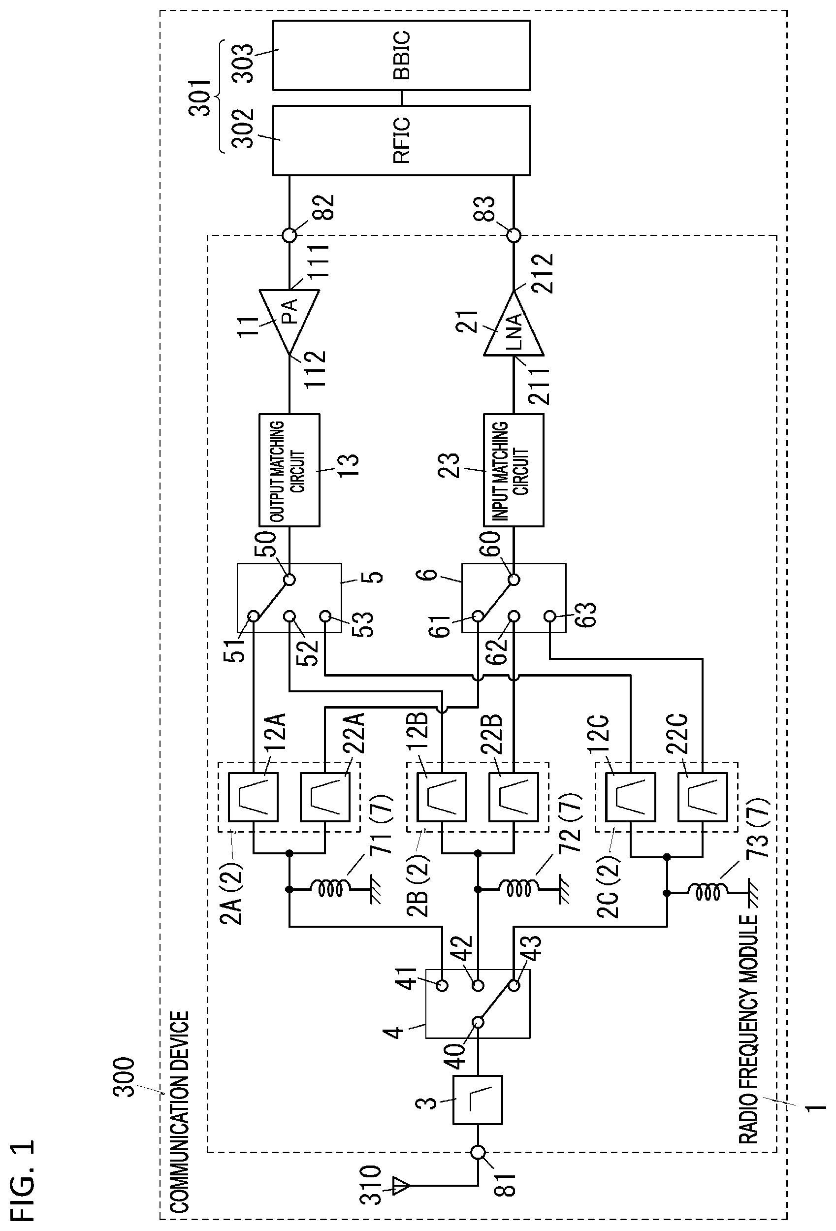
is a circuit configuration diagram of a communication device including a radio frequency module according to a first embodiment.
is a circuit configuration diagram of an attenuation filter of the radio frequency module according to the first embodiment.
is a schematic plan view illustrating the arrangement of individual constituent elements of the radio frequency module according to the first embodiment.
is a diagram for describing characteristics of the radio frequency module according to the first embodiment.
is a schematic plan view illustrating the arrangement of individual constituent elements of a radio frequency module according to a first modification of the first embodiment.
is a circuit configuration diagram of a communication device including a radio frequency module according to a second embodiment.
is a circuit configuration diagram of an attenuation filter of the radio frequency module according to the second embodiment.
is a schematic plan view illustrating the arrangement of individual constituent elements of the radio frequency module according to the second embodiment.
DETAILED DESCRIPTION OF THE DISCLOSURE
Both of , to which reference will be made in a first embodiment and so forth below, are schematic diagrams. The ratios between the sizes and thicknesses of the individual constituent elements in the drawings may not necessarily reflect the actual dimensional ratios.
First Embodiment
In the following, a radio frequency module 1 and a communication device 300 according to the first embodiment will be described with reference to to 4 .
(1) Overall Configuration of Radio Frequency Module
The radio frequency module 1 according to the present embodiment is used in, for example, the communication device 300 , which is a multimode or multiband communication device. The communication device 300 is, for example, a cellular phone (for example, a smartphone) but not limited to this and may be, for example, a wearable terminal (for example, a smartwatch) or the like. The radio frequency module 1 is a module that can accommodate, for example, the fourth generation mobile communication (4G) standards, the fifth generation mobile communication (5G) standards, and so forth. The 4G standards are, for example, the 3GPP Long Term Evolution (LTE) standards. The 5G standards are, for example, 5G New Radio (NR). The radio frequency module 1 is a module that can support carrier aggregation and dual connectivity.
The radio frequency module 1 is configured to, for example, amplify a transmission signal inputted from a signal processing circuit 301 and output the resulting signal to an antenna 310 . In addition, the radio frequency module 1 is configured to amplify a reception signal inputted from the antenna 310 and output the resulting signal to the signal processing circuit 301 . The signal processing circuit 301 is not a constituent element of the radio frequency module 1 but a constituent element of the communication device 300 including the radio frequency module 1 . The radio frequency module 1 according to the first embodiment is controlled by, for example, the signal processing circuit 301 included in the communication device 300 . The communication device 300 includes the radio frequency module 1 and the signal processing circuit 301 . The communication device 300 further includes the antenna 310 . The signal processing circuit 301 processes a reception signal received through the antenna 310 .
The radio frequency module 1 according to the present embodiment includes a mounting board 9 (see ), a switch 4 , an attenuation filter 3 , and a plurality of band pass filters (a first transmission filter 12 A, a second transmission filter 12 B, a third transmission filter 12 C, a first reception filter 22 A, a second reception filter 22 B, and a third reception filter 22 C). The attenuation filter 3 is, for example, a low pass filter.
The switch 4 is mounted on the mounting board 9 and has a common terminal 40 , which is connected to an antenna terminal 81 , and a plurality of selection terminals 41 to 43 , which are to be connected to the common terminal 40 . The switch 4 is a switch that can simultaneously connect the common terminal 40 to at least the selection terminal (a first selection terminal) 41 and the selection terminal (a second selection terminal) 42 out of the plurality of selection terminals 41 to 43 . The attenuation filter 3 is mounted on the mounting board 9 and is connected between the common terminal 40 and the antenna terminal 81 . The plurality of band pass filters are mounted on the mounting board 9 and are connected to the plurality of selection terminals 41 to 43 . The plurality of band pass filters have a first band pass filter (the first reception filter 22 A) and a second band pass filter (the second reception filter 22 B). The first band pass filter is connected to the first selection terminal 41 and is a filter having a pass band, which is a first frequency band. The second band pass filter is connected to the second selection terminal 42 and is a filter having a pass band, which is a second frequency band, which is higher than the first frequency band. The attenuation filter 3 is a low pass filter or a notch filter including at least one reactive element out of an inductive element (for example, an inductor 32 ) and a capacitive element (for example, a capacitor 35 ) (shown in ).
In the radio frequency module 1 , the reactive element described above (for example, the inductor 32 ) is adjacent to at least one band pass filter (for example, the first reception filter 22 A) out of the plurality of band pass filters. In the present specification and so forth, “adjacent” indicates that another electronic component is not present between two adjacent electronic components.
In the radio frequency module 1 and the communication device 300 according to the present embodiment, the plurality of band pass filters have the first band pass filter and the second band pass filter. The reactive element described above and included in the attenuation filter 3 is adjacent to at least one band pass filter out of the plurality of band pass filters. Consequently, the reactive element described above and a portion of the at least one band pass filter out of the plurality of band pass filters (for example, a bump 24 ) can be magnetically or capacitively coupled with each other. As a result, the pass band of the attenuation filter 3 can be shifted to the low frequency side such that a harmonic wave component of a signal (a reception signal) that passes through the first band pass filter (for example, the first reception filter 22 A), which is a band pass filter corresponding to relatively low frequencies, does not pass through the attenuation filter 3 . Consequently, the degradation of the filter characteristic of the second band pass filter, which is a band pass filter corresponding to relatively high frequencies, due to the harmonic wave component of a signal that passes through the first band pass filter, which is a band pass filter corresponding to relatively low frequencies, can be suppressed.
(2) Individual Constituent Elements of Radio Frequency Module
The radio frequency module 1 according to the present embodiment includes a power amplifier 11 , a low noise amplifier 21 , a plurality of filter units 2 (three filter units in the illustrated example), the attenuation filter 3 , and a matching circuit 7 as illustrated in . Moreover, the radio frequency module 1 includes an output matching circuit 13 , an input matching circuit 23 , a first switch 4 , a second switch 5 , and a third switch 6 . In the following description, in a case where the plurality of filter units 2 are distinguished from each other, the plurality of filter units 2 are also individually called “first filter unit 2 A”, “second filter unit 2 B”, and “third filter unit 2 C”.
(2.1) Power Amplifier
The power amplifier 11 has an input terminal 111 and an output terminal 112 . The power amplifier 11 amplifies transmission signals of a first communication band, a second communication band, and a third communication band inputted to the input terminal 111 and outputs the amplified transmission signals from the output terminal 112 . The first communication band corresponds to a transmission signal passing through the first transmission filter 12 A and is, for example, Band 12 . The second communication band corresponds to a transmission signal passing through the second transmission filter 12 B and is, for example, Band 14 . The third communication band corresponds to a transmission signal passing through the third transmission filter 12 C and is, for example, Band 26 . The output terminal 112 of the power amplifier 11 is connected to a common terminal 50 of the second switch 5 with the output matching circuit 13 interposed therebetween. The input terminal 111 of the power amplifier 11 is connected to a signal input terminal 82 . The input terminal 111 of the power amplifier 11 is connected to, for example, the signal processing circuit 301 with the signal input terminal 82 interposed therebetween. The signal input terminal 82 is a terminal for inputting a radio frequency signal (transmission signal) from an external circuit (for example, the signal processing circuit 301 ) to the radio frequency module 1 .
(2.2) Low Noise Amplifier
The low noise amplifier 21 has an input terminal 211 and an output terminal 212 . The low noise amplifier 21 amplifies reception signals of a fourth communication band, a fifth communication band, and a sixth communication band inputted to the input terminal 211 and outputs the amplified reception signals from the output terminal 212 . The fourth communication band corresponds to a reception signal passing through the first reception filter 22 A and is, for example, Band 12 . The fifth communication band corresponds to a reception signal passing through the second reception filter 22 B and is, for example, Band 14 . The sixth communication band corresponds to a reception signal passing through the third reception filter 22 C and is, for example, Band 26 . The input terminal 211 of the low noise amplifier 21 is connected to a common terminal 60 of the third switch 6 with the input matching circuit 23 interposed therebetween. The output terminal 212 of the low noise amplifier 21 is connected to a signal output terminal 83 . The output terminal 212 of the low noise amplifier 21 is connected to, for example, the signal processing circuit 301 with the signal output terminal 83 interposed therebetween. The signal output terminal 83 is a terminal for outputting a radio frequency signal (reception signal) from the low noise amplifier 21 to an external circuit (for example, the signal processing circuit 301 ).
In the present embodiment, for example, the reception band of the fourth communication band is the first frequency band, and the reception band of the fifth communication band is the second frequency band.
(2.3) First Filter Unit
The first filter unit 2 A includes the first transmission filter 12 A and the first reception filter 22 A. That is, in the first filter unit 2 A, the first transmission filter 12 A and the first reception filter 22 A are integrated on one chip (see ). The first transmission filter 12 A is, for example, a filter having a pass band, which is the transmission band of the first communication band. The first reception filter 22 A is, for example, a filter having a pass band, which is the reception band of the fourth communication band. That is, in the present embodiment, the first reception filter 22 A is the first band pass filter having a pass band, which is the first frequency band.
Each of the first transmission filter 12 A and the first reception filter 22 A is, for example, an acoustic wave filter. In each of the first transmission filter 12 A and the first reception filter 22 A, a plurality of series arm resonators and a plurality of parallel arm resonators each include an acoustic wave resonator. The acoustic wave resonator is, for example, a surface acoustic wave (SAW) resonator.
The SAW resonator includes, for example, a piezoelectric substrate and an interdigital transducer (IDT) electrode provided on the piezoelectric substrate. In a case where each of the plurality of series arm resonators and the plurality of parallel arm resonators is formed to include a SAW resonator, each of the first transmission filter 12 A and the first reception filter 22 A has a plurality of interdigital transducer (IDT) electrodes corresponding to the plurality of series arm resonators in a one-to-one relationship and a plurality of IDT electrodes corresponding to the plurality of parallel arm resonators in a one-to-one relationship on one piezoelectric substrate. The piezoelectric substrate is, for example, a lithium tantalate substrate or a lithium niobate substrate.
(2.4) Second Filter Unit
The second filter unit 2 B includes the second transmission filter 12 B and the second reception filter 22 B. That is, in the second filter unit 2 B, the second transmission filter 12 B and the second reception filter 22 B are integrated on one chip (see ). The second transmission filter 12 B is, for example, a filter having a pass band, which is the transmission band of the second communication band. The second reception filter 22 B is, for example, a filter having a pass band, which is the reception band of the fifth communication band. That is, in the present embodiment, the second reception filter 22 B is the second band pass filter having a pass band, which is the second frequency band, which is higher than the first frequency band.
Each of the second transmission filter 12 B and the second reception filter 22 B is, for example, an acoustic wave filter. In each of the second transmission filter 12 B and the second reception filter 22 B, a plurality of series arm resonators and a plurality of parallel arm resonators each include an acoustic wave resonator. The acoustic wave resonator is, for example, a SAW resonator.
(2.5) Third Filter Unit
The third filter unit 2 C includes the third transmission filter 12 C and the third reception filter 22 C. That is, in the third filter unit 2 C, the third transmission filter 12 C and the third reception filter 22 C are integrated on one chip (see ). The third transmission filter 12 C is, for example, a filter having a pass band, which is the transmission band of the third communication band. The third reception filter 22 C is, for example, a filter having a pass band, which is the reception band of the sixth communication band.
Each of the third transmission filter 12 C and the third reception filter 22 C is, for example, an acoustic wave filter. In each of the third transmission filter 12 C and the third reception filter 22 C, a plurality of series arm resonators and a plurality of parallel arm resonators each include an acoustic wave resonator. The acoustic wave resonator is, for example, a SAW resonator.
In the radio frequency module 1 , the plurality of band pass filters are constituted by the first transmission filter 12 A, the second transmission filter 12 B, the third transmission filter 12 C, the first reception filter 22 A, the second reception filter 22 B, and the third reception filter 22 C.
(2.6) First Switch
The first switch 4 has the common terminal 40 and the plurality of selection terminals 41 to 43 (three selection terminals in the illustrated example). The common terminal 40 is connected to the antenna terminal 81 with the attenuation filter 3 interposed therebetween. The antenna 310 is connected to the antenna terminal 81 . The selection terminal 41 is connected to a connection point connecting an output terminal of the first transmission filter 12 A to an input terminal of the first reception filter 22 A. The selection terminal 42 is connected to a connection point connecting an output terminal of the second transmission filter 12 B to an input terminal of the second reception filter 22 B. The selection terminal 43 is connected to a connection point connecting an output terminal of the third transmission filter 12 C to an input terminal of the third reception filter 22 C. The first switch 4 is a switch that can simultaneously connect, for example, at least the selection terminals 41 and 42 out of the plurality of selection terminals 41 to 43 to the common terminal 40 . That is, the first switch 4 is a switch that allows one-to-many connections.
The first switch 4 is controlled by, for example, the signal processing circuit 301 . The first switch 4 switches a connection state between the common terminal 40 and the plurality of selection terminals 41 to 43 in accordance with a control signal from a radio frequency (RF) signal processing circuit 302 of the signal processing circuit 301 . The first switch 4 is, for example, a switch integrated circuit (IC).
(2.7) Second Switch
The second switch 5 has the common terminal 50 and a plurality of selection terminals 51 to 53 (three selection terminals in the illustrated example). The common terminal 50 is connected to the output terminal 112 of the power amplifier 11 with the output matching circuit 13 interposed therebetween. The selection terminal 51 is connected to an input terminal of the first transmission filter 12 A. The selection terminal 52 is connected to an input terminal of the second transmission filter 12 B. The selection terminal 53 is connected to an input terminal of the third transmission filter 12 C. The second switch 5 is a switch that can simultaneously connect, for example, at least two or more selection terminals out of the plurality of selection terminals 51 to 53 to the common terminal 50 . That is, the second switch 5 is a switch that allows one-to-many connections.
The second switch 5 is controlled by, for example, the signal processing circuit 301 . The second switch 5 switches a connection state between the common terminal 50 and the plurality of selection terminals 51 to 53 in accordance with a control signal from the RF signal processing circuit 302 of the signal processing circuit 301 . The second switch 5 is, for example, a switch IC.
(2.8) Third Switch
The third switch 6 has the common terminal 60 and a plurality of selection terminals 61 to 63 (three selection terminals in the illustrated example). The common terminal 60 is connected to the input terminal 211 of the low noise amplifier 21 with the input matching circuit 23 interposed therebetween. The selection terminal 61 is connected to an output terminal of the first reception filter 22 A. The selection terminal 62 is connected to an output terminal of the second reception filter 22 B. The selection terminal 63 is connected to an output terminal of the third reception filter 22 C. The third switch 6 is a switch that can simultaneously connect, for example, at least two or more selection terminals out of the plurality of selection terminals 61 to 63 to the common terminal 60 . That is, the third switch 6 is a switch that allows one-to-many connections.
The third switch 6 is controlled by, for example, the signal processing circuit 301 . The third switch 6 switches a connection state between the common terminal 60 and the plurality of selection terminals 61 to 63 in accordance with a control signal from the RF signal processing circuit 302 of the signal processing circuit 301 . The third switch 6 is, for example, a switch IC.
(2.9) Attenuation Filter
The attenuation filter 3 is provided along a signal path between the antenna terminal 81 and the common terminal 40 of the first switch 4 . The attenuation filter 3 attenuates a harmonic wave component of a reception signal received through the antenna 310 . The attenuation filter 3 is, for example, a low pass filter. The attenuation filter 3 is, for example, a filter having a pass band, which is the reception band of Band 1 .
As illustrated in , the attenuation filter 3 has a plurality of inductors 31 to 33 (three inductors in the illustrated example), a plurality of capacitors 34 to 36 (three capacitors in the illustrated example), an input terminal 37 , and an output terminal 38 .
The inductor 31 and the capacitor 34 are connected in parallel and form a parallel circuit 391 . The parallel circuit 391 is provided between the input terminal 37 and a node N 1 on a path P 1 between the input terminal 37 and the output terminal 38 .
The inductor 32 and the capacitor 35 are connected in parallel and form a parallel circuit 392 . The parallel circuit 392 is provided between the node N 1 and the output terminal 38 . The parallel circuit 392 is connected in series with the parallel circuit 391 on the path P 1 . That is, in the attenuation filter 3 , the parallel circuit 391 is positioned on the input terminal 37 side, and the parallel circuit 392 is positioned on the output terminal 38 side on the path P 1 .
The inductor 33 and the capacitor 36 are connected in series and form a series circuit 393 . The series circuit 393 is provided between the node N 1 and ground.
(2.10) Output Matching Circuit
The output matching circuit 13 is provided along a signal path between the output terminal 112 of the power amplifier 11 and the common terminal 50 of the second switch 5 . The output matching circuit 13 is a circuit for achieving impedance matching between the first, second, and third transmission filters 12 A, 12 B, and 12 C and the power amplifier 11 . The output matching circuit 13 includes, for example, one inductor but not limited to this. The output matching circuit 13 may include a plurality of inductors and a plurality of capacitors.
(2.11) Input Matching Circuit
The input matching circuit 23 is provided along a signal path between the input terminal 211 of the low noise amplifier 21 and the common terminal 60 of the third switch 6 . The input matching circuit 23 is a circuit for achieving impedance matching between the first, second, and third reception filters 22 A, 22 B, and 22 C and the low noise amplifier 21 . The input matching circuit 23 includes, for example, one inductor but not limited to this. The input matching circuit 23 may include a plurality of inductors and a plurality of capacitors.
(2.12) Matching Circuit
The matching circuit 7 has a plurality of inductors 71 to 73 (three inductors in the illustrated example).
The inductor 71 is an inductor for achieving impedance matching between the first filter unit 2 A, which in other words is the first transmission filter 12 A and the first reception filter 22 A, and the attenuation filter 3 . The inductor 71 is provided, for example, along a signal path between the connection point connecting the output terminal of the first transmission filter 12 A to the input terminal of the first reception filter 22 A and the selection terminal 41 of the first switch 4 . The inductor 71 is connected between the signal path and ground.
The inductor 72 is an inductor for achieving impedance matching between the second filter unit 2 B, which in other words is the second transmission filter 12 B and the second reception filter 22 B, and the attenuation filter 3 . The inductor 72 is provided, for example, along a signal path between the connection point connecting the output terminal of the second transmission filter 12 B to the input terminal of the second reception filter 22 B and the selection terminal 42 of the first switch 4 . The inductor 72 is connected between the signal path and ground.
The inductor 73 is an inductor for achieving impedance matching between the third filter unit 2 C, which in other words is the third transmission filter 12 C and the third reception filter 22 C, and the attenuation filter 3 . The inductor 73 is provided, for example, along a signal path between the connection point connecting the output terminal of the third transmission filter 12 C to the input terminal of the third reception filter 22 C and the selection terminal 43 of the first switch 4 . The inductor 73 is connected between the signal path and ground.
(3) Communication Device
The communication device 300 includes the radio frequency module 1 described above and the signal processing circuit 301 as illustrated in . The communication device 300 further includes the antenna 310 . The signal processing circuit 301 includes the RF signal processing circuit 302 and a baseband signal processing circuit 303 . In the present embodiment, the RF signal processing circuit 302 and the baseband signal processing circuit 303 form a signal processing circuit that processes a first signal and a second signal.
(3.1) RF Signal Processing Circuit
The RF signal processing circuit 302 is, for example, an RF integrated circuit (RFIC) and performs signal processing on a radio frequency signal. The RF signal processing circuit 302 performs signal processing such as upconversion on, for example, a radio frequency signal (a transmission signal) outputted from the baseband signal processing circuit 303 and outputs the radio frequency signal subjected to the signal processing.
(3.2) Baseband Signal Processing Circuit
The baseband signal processing circuit 303 is, for example, a baseband integrated circuit (BBIC) and performs predetermined signal processing on a transmission signal from outside the signal processing circuit 301 . The reception signal processed by the baseband signal processing circuit 303 is used, for example, as an image signal for image display or as an audio signal for a telephone call. The radio frequency module 1 transfers a radio frequency signal (a reception signal, a transmission signal) between the antenna 310 and the RF signal processing circuit 302 of the signal processing circuit 301 . In the communication device 300 , the baseband signal processing circuit 303 is an inessential constituent element.
(4) Arrangement of Individual Constituent Elements of Radio Frequency Module
Next, the arrangement of individual constituent elements of the radio frequency module 1 on the mounting board 9 will be described with reference to . In the following description, up-down and left-right directions are each defined as the directions illustrated in . That is, in an example illustrated in , the direction in which the first filter unit 2 A and the second filter unit 2 B are aligned corresponds to the up-down direction (the first filter unit 2 A is on the upper side), and the direction in which the first switch 4 and the attenuation filter 3 are aligned corresponds to the left-right direction (the first switch 4 is on the left).
The radio frequency module 1 according to the present embodiment further includes the mounting board 9 as illustrated in . The mounting board 9 has a rectangular shape when viewed in a plan view from the thickness direction of the mounting board 9 (the direction perpendicular to the sheet of ). The mounting board 9 has a first main surface 91 and a second main surface 92 . The first main surface 91 and the second main surface 92 face with each other in the thickness direction of the mounting board 9 . The mounting board 9 is, for example, a printed wiring board or a low temperature co-fired ceramics (LTCC) substrate.
The mounting board 9 is, for example, a multi-layer substrate including a plurality of dielectric layers and a plurality of conductive pattern layers. The plurality of dielectric layers and the plurality of conductive pattern layers are stacked in the thickness direction of the mounting board 9 . The plurality of conductive pattern layers are each formed to have a predetermined pattern. Each of the plurality of conductive pattern layers includes one or more conductor portions in a plane perpendicular to the thickness direction of the mounting board 9 . A material of each conductive pattern layer is, for example, copper. The plurality of conductive pattern layers include a ground layer.
In the radio frequency module 1 , the first filter unit 2 A, the second filter unit 2 B, the attenuation filter 3 , the first switch 4 , and the inductors 71 and 72 of the matching circuit 7 described above are mounted on the first main surface 91 of the mounting board 9 . Note that the third filter unit 2 C, the second switch 5 , the third switch 6 , the inductor 73 of the matching circuit 7 , the power amplifier 11 , the low noise amplifier 21 , the output matching circuit 13 , and the input matching circuit 23 described above are mounted on the first main surface 91 or the second main surface 92 of the mounting board 9 although the illustration thereof is omitted.
The attenuation filter 3 is mounted substantially on the center of the first main surface 91 of the mounting board 9 . In the attenuation filter 3 , the inductors 31 and 32 and the capacitors 34 and 35 included in the attenuation filter 3 are arranged in the order of the inductor 32 , the capacitor 35 , the inductor 31 , and the capacitor 34 from the top side. Each of the inductors 31 and 32 and the capacitors 34 and 35 is connected to the first main surface 91 of the mounting board 9 by a connection portion 30 . The connection portion 30 is, for example, solder. Note that as with the inductors 31 and 32 and the capacitors 34 and 35 , the inductor 33 and the capacitor 36 included in the attenuation filter 3 are connected to the first main surface 91 of the mounting board 9 by the connection portions 30 although the illustration thereof is omitted.
The first switch 4 is mounted to the left of the attenuation filter 3 on the first main surface 91 of the mounting board 9 . The first switch 4 is connected to the first main surface 91 of the mounting board 9 with, for example, solder.
The first filter unit 2 A and the second filter unit 2 B are mounted to the right of the attenuation filter 3 on the first main surface 91 of the mounting board 9 . The first filter unit 2 A and the second filter unit 2 B are aligned with a space therebetween in the up-down direction such that the first filter unit 2 A is positioned on the upper side and the second filter unit 2 B is positioned on the lower side. Each of the first filter unit 2 A and the second filter unit 2 B is connected to the first main surface 91 of the mounting board 9 by a plurality of connection portions 24 . The connection portions 24 are, for example, solder bumps but may also be gold bumps.
On the first main surface 91 of the mounting board 9 , the inductor 71 of the matching circuit 7 is mounted above the first filter unit 2 A. That is, the first filter unit 2 A and the inductor 71 are aligned with a space therebetween in the up-down direction such that the inductor 71 is positioned on the upper side and the first filter unit 2 A is positioned on the lower side. On the first main surface 91 of the mounting board 9 , the inductor 72 of the matching circuit 7 is mounted above the second filter unit 2 B. That is, the second filter unit 2 B and the inductor 72 are aligned with a space therebetween in the up-down direction such that the inductor 72 is positioned on the upper side and the second filter unit 2 B is positioned on the lower side. Thus, in the radio frequency module 1 , the first filter unit 2 A, the second filter unit 2 B, and the inductors 71 and 72 are aligned in the order of the inductor 71 , the first filter unit 2 A, the inductor 72 , and the second filter unit 2 B from the top side. Each of the inductors 71 and 72 is connected to the first main surface 91 of the mounting board 9 by a connection portion 70 . The connection portion 70 is, for example, solder.
(5) Characteristics of Radio Frequency Module
Next, characteristics of the radio frequency module 1 will be described with reference to . In , “PB 1 ” denotes the pass band of the first reception filter 22 A, “PB 2 ” denotes the pass band of the second reception filter 22 B, and “PB 3 ” denotes the pass band of the third reception filter 22 C. Moreover, in , “PB 4 ” denotes the pass band of an attenuation filter according to a comparative example, and “PB 5 ” denotes the pass band of the attenuation filter 3 according to the present embodiment. Furthermore, in , “HA 1 ” denotes a harmonic wave (for example, a second harmonic wave) of a reception signal that passes through the first reception filter 22 A, and “HA 2 ” denotes a harmonic wave (for example, a second harmonic wave) of a reception signal that passes through the third reception filter 22 C. Note that a solid line representing the pass band PB 4 and a broken line representing the pass band PB 5 are shifted from each other and illustrated in the drawing so that the lines are easy to be distinguished from each other; however, in reality, the straight sections extending in the horizontal axis direction at least partially overlap.
In the radio frequency module 1 according to the present embodiment, the reception band of Band 12 is treated as the pass band of the fourth communication band, which is the communication band of the first reception filter 22 A, the reception band of Band 14 is treated as the pass band of the fifth communication band, which is the communication band of the second reception filter 22 B, and the reception band of Band 26 is treated as the pass band of the sixth communication band, which is the communication band of the third reception filter 22 C. Thus, the pass bands PB 1 , PB 2 , and PB 3 are arranged in the order of the pass band PB 1 , the pass band PB 2 , and the pass band PB 3 from the low frequency side.
In the attenuation filter according to the comparative example, a harmonic wave HA′ of a reception signal that passes through the first reception filter 22 A is included in the pass band PB 4 . Thus, for example, in a case where the harmonic wave HA′ overlaps an attenuation region of the second reception filter 22 B, the filter characteristic of the second reception filter 22 B is degraded. Note that even in this case, a harmonic wave HA 2 of a reception signal that passes through the third reception filter 22 C is not included in the pass band PB 4 of the attenuation filter according to the comparative example. Thus, the filter characteristic of the second reception filter 22 B is not degraded by the harmonic wave HA 2 .
In the radio frequency module 1 according to the present embodiment, for example, the inductor 32 (an inductive element) and the capacitor 35 (a capacitive element) included in the attenuation filter 3 are adjacent to the first filter unit 2 A (the first reception filter 22 A) in a plan view from the thickness direction of the mounting board 9 as illustrated in . That is, in , another electronic component is not present between the inductor 32 and capacitor 35 of the attenuation filter 3 and the first reception filter 22 A. In the radio frequency module 1 , the inductor 31 included in the attenuation filter 3 is adjacent to the inductor 72 of the matching circuit 7 . That is, in , another electronic component is not present between the inductor 31 of the attenuation filter 3 and the inductor 72 of the matching circuit 7 . Furthermore, in the radio frequency module 1 , the capacitor 34 included in the attenuation filter 3 is adjacent to the second filter unit 2 B (the second reception filter 22 B). That is, in , another electronic component is not present between the capacitor 34 of the attenuation filter 3 and the second reception filter 22 B. In the present embodiment, for example, the connection portions 24 for connecting the first reception filter 22 A to the mounting board 9 are adjacent to the inductor 32 and the capacitor 35 . Moreover, for example, the connection portions 24 for connecting the second reception filter 22 B to the mounting board 9 are adjacent to the capacitor 34 . In the present embodiment, the inductor 32 included in the attenuation filter 3 is a reactive element.
Here, in a case where the distance between the inductor 32 of the attenuation filter 3 and the connection portions 24 of the first reception filter 22 A is denoted by d 1 and the stray capacitance between the inductor 32 and the connection portions 24 is denoted by C 1 , the stray capacitance C 1 is inversely proportional to the distance d 1 , and thus the shorter the distance d 1 , the greater the stray capacitance C 1 . In a case where the resonant frequency of the attenuation filter 3 is denoted by f 1 , the resonant frequency f 1 is inversely proportional to the stray capacitance C 1 , and thus the greater the stray capacitance C 1 , the lower the resonant frequency f 1 . Thus, by reducing the distance d 1 between the inductor 32 of the attenuation filter 3 and the connection portions 24 of the first reception filter 22 A, the pass band PB 5 of the attenuation filter 3 can be shifted to the low frequency side (see ). That is, the pass band PB 5 of the attenuation filter 3 can be shifted to the low frequency side by capacitively coupling the inductor 32 (an inductive element) of the attenuation filter 3 with the connection portions 24 of the first reception filter 22 A. Note that substantially the same applies to the inductor 31 and the capacitors 34 and 35 included in the attenuation filter 3 .
As described above, by shifting the pass band PB 5 of the attenuation filter 3 to the low frequency side, a harmonic wave component HA 1 of a reception signal that passes through the first reception filter 22 A is blocked by the attenuation filter 3 . Consequently, the degradation of the filter characteristic of the second reception filter 22 B, which corresponds to relatively high frequencies, due to the harmonic wave component HA 1 of a reception signal that passes through the first reception filter 22 A, which corresponds to relatively low frequencies, can be suppressed.
(6) Modification
In the following, a modification of the radio frequency module 1 according to the first embodiment will be described.
(6.1) First Modification
A radio frequency module 1 according to a first modification of the first embodiment will be described with reference to . Regarding the radio frequency module 1 according to the first modification, the constituent elements substantially the same as those of the radio frequency module 1 according to the first embodiment will be denoted by the same reference numerals, and the description thereof will be omitted.
The radio frequency module 1 according to the first modification differs from the radio frequency module 1 according to the first embodiment in that the attenuation filter 3 including a plurality of reactive elements (the inductors 31 to 33 and the capacitors 34 to 36 ) is formed as one chip 10 .
In the radio frequency module 1 according to the first modification, in a case where the mounting board 9 is viewed in a plan view, the chip 10 including the plurality of reactive elements is adjacent to the first filter unit 2 A. In the example illustrated in , the distance between the chip 10 and the first filter unit 2 A is d 11 . In this manner, by causing the chip 10 including the attenuation filter 3 to be adjacent to the first filter unit 2 A, the degradation of the filter characteristic of a band pass filter corresponding to relatively high frequencies (for example, the second reception filter 22 B) due to a harmonic wave component of a signal that passes through a band pass filter corresponding to relatively low frequencies (for example, the first reception filter 22 A) can be suppressed.
(6.2) Another Modification
The radio frequency module 1 in the first embodiment includes the first transmission filter 12 A, the second transmission filter 12 B, the third transmission filter 12 C, the first reception filter 22 A, the second reception filter 22 B, and the third reception filter 22 C as the plurality of band pass filters. In contrast to this, the radio frequency module 1 may include only the first reception filter 22 A, the second reception filter 22 B, and the third reception filter 22 C, which are reception filters, as the plurality of band pass filters. In this case, it is sufficient that the number of reception filters included in the radio frequency module 1 be at least one.
In the first embodiment, the number of attenuation filters 3 provided between the antenna 310 and the first switch 4 is one; however, for example, a plurality of attenuation filters may be provided between the antenna 310 and the first switch 4 .
In the first embodiment, the inductors 31 and 32 and the capacitors 34 and 35 constituting a portion of the attenuation filter 3 are made adjacent to the first reception filter 22 A, the second reception filter 22 B, or the inductor 72 of the matching circuit 7 . In contrast to this, at least one out of the inductors 31 , 32 , and 33 and the capacitors 34 , 35 , and 36 included in the attenuation filter 3 may be made adjacent to the first reception filter 22 A, the second reception filter 22 B, or the inductor 72 of the matching circuit 7 .
Second Embodiment
A radio frequency module 1 A and a communication device 300 A according to a second embodiment will be described with reference to to 8 .
The communication device 300 A according to the present embodiment includes the radio frequency module 1 A and the signal processing circuit 301 as illustrated in . The communication device 300 A further includes the antenna 310 . The signal processing circuit 301 includes the RF signal processing circuit 302 and the baseband signal processing circuit 303 . Note that the signal processing circuit 301 and the antenna 310 are substantially the same as those of the communication device 300 according to the first embodiment, and thus only the radio frequency module 1 A will be described in the following.
(1) Configuration of Radio Frequency Module
The radio frequency module 1 A according to the second embodiment includes the power amplifier 11 , the low noise amplifier 21 , a plurality of filter units 2 (four filter units in the illustrated example), an attenuation filter 3 A, and a matching circuit 7 A as illustrated in . Moreover, the radio frequency module 1 A includes the output matching circuit 13 , the input matching circuit 23 , a plurality of first switches 4 A and 4 B (two switches in the illustrated example), a second switch 5 A, a third switch 6 A, and a multiplexer 14 . In the following description, in a case where the plurality of filter units 2 are distinguished from each other, the plurality of filter units 2 are also individually called “first filter unit 2 A”, “second filter unit 2 B”, “third filter unit 2 C”, and “fourth filter unit 2 D”. The power amplifier 11 , the low noise amplifier 21 , the output matching circuit 13 , and the input matching circuit 23 are substantially the same as those of the radio frequency module 1 according to the first embodiment, and thus the description thereof will be omitted here.
(1.1) First Filter Unit
The first filter unit 2 A includes the first transmission filter 12 A and the first reception filter 22 A. That is, in the first filter unit 2 A, the first transmission filter 12 A and the first reception filter 22 A are integrated on one chip (see ). The first transmission filter 12 A is, for example, a filter having a pass band, which is the transmission band of a first communication band. The first reception filter 22 A is, for example, a filter having a pass band, which is the reception band of the first communication band. The first communication band is, for example, Band 12 .
(1.2) Second Filter Unit
The second filter unit 2 B includes the second transmission filter 12 B and the second reception filter 22 B. That is, in the second filter unit 2 B, the second transmission filter 12 B and the second reception filter 22 B are integrated on one chip (see ). The second transmission filter 12 B is, for example, a filter having a pass band, which is the transmission band of a second communication band. The second reception filter 22 B is, for example, a filter having a pass band, which is the reception band of the second communication band. The second communication band is, for example, Band 26 .
(1.3) Third Filter Unit
The third filter unit 2 C includes the third transmission filter 12 C and the third reception filter 22 C. That is, in the third filter unit 2 C, the third transmission filter 12 C and the third reception filter 22 C are integrated on one chip (see ). The third transmission filter 12 C is, for example, a filter having a pass band, which is the transmission band of a third communication band. The third reception filter 22 C is, for example, a filter having a pass band, which is the reception band of the third communication band. The third communication band is, for example, Band 11 .
(1.4) Fourth Filter Unit
The fourth filter unit 2 D includes a fourth transmission filter 12 D and a fourth reception filter 22 D. That is, in the fourth filter unit 2 D, the fourth transmission filter 12 D and the fourth reception filter 22 D are integrated on one chip (see ). The fourth transmission filter 12 D is, for example, a filter having a pass band, which is the transmission band of a fourth communication band. The fourth reception filter 22 D is, for example, a filter having a pass band, which is the reception band of the fourth communication band. The fourth communication band is, for example, Band 3 . In the radio frequency module 1 A, the plurality of band pass filters are constituted by the first transmission filter 12 A, the second transmission filter 12 B, the third transmission filter 12 C, the fourth transmission filter 12 D, the first reception filter 22 A, the second reception filter 22 B, the third reception filter 22 C, and the fourth reception filter 22 D.
(1.5) First Switches
Each of the plurality of first switches 4 A and 4 B has the common terminal 40 and the two selection terminals 41 and 42 .
The common terminal 40 of the first switch 4 A is connected to the antenna terminal 81 with the attenuation filter 3 A and the multiplexer 14 interposed therebetween. The antenna 310 is connected to the antenna terminal 81 . The selection terminal (the first selection terminal) 41 is connected to the connection point connecting the output terminal of the first transmission filter 12 A to the input terminal of the first reception filter 22 A. The selection terminal (the second selection terminal) 42 is connected to the connection point connecting the output terminal of the second transmission filter 12 B to the input terminal of the second reception filter 22 B. The first switch 4 A is a switch that can simultaneously connect, for example, the two selection terminals 41 and 42 to the common terminal 40 . That is, the first switch 4 A is a switch that allows one-to-many connections.
The common terminal 40 of the first switch 4 B is connected to the antenna terminal 81 with the multiplexer 14 interposed therebetween. The selection terminal (the first selection terminal) 41 is connected to the connection point connecting the output terminal of the third transmission filter 12 C to the input terminal of the third reception filter 22 C. The selection terminal (the second selection terminal) 42 is connected to a connection point connecting an output terminal of the fourth transmission filter 12 D to an input terminal of the fourth reception filter 22 D. The first switch 4 B is a switch that can simultaneously connect, for example, the two selection terminals 41 and 42 to the common terminal 40 . That is, the first switch 4 B is a switch that allows one-to-many connections.
Each of the plurality of first switches 4 A and 4 B is controlled by, for example, the signal processing circuit 301 . Each of the plurality of first switches 4 A and 4 B switches a connection state between the common terminal 40 and the two selection terminals 41 and 42 in accordance with a control signal from the RF signal processing circuit 302 of the signal processing circuit 301 . Each of the plurality of first switches 4 A and 4 B is, for example, a switch IC.
(1.6) Second Switch
The second switch 5 A has the common terminal 50 and four selection terminals 51 to 54 . The common terminal 50 is connected to the output terminal 112 of the power amplifier 11 with the output matching circuit 13 interposed therebetween. The selection terminal 51 is connected to the input terminal of the first transmission filter 12 A. The selection terminal 52 is connected to the input terminal of the second transmission filter 12 B. The selection terminal 53 is connected to the input terminal of the third transmission filter 12 C. The selection terminal 54 is connected to an input terminal of the fourth transmission filter 12 D. The second switch 5 A is a switch that can simultaneously connect, for example, at least two or more out of the four selection terminals 51 to 54 to the common terminal 50 . That is, the second switch 5 A is a switch that allows one-to-many connections.
The second switch 5 A is controlled by, for example, the signal processing circuit 301 . The second switch 5 A switches a connection state between the common terminal 50 and the four selection terminals 51 to 54 in accordance with a control signal from the RF signal processing circuit 302 of the signal processing circuit 301 . The second switch 5 A is, for example, a switch IC.
(1.7) Third Switch
The third switch 6 A has the common terminal 60 and four selection terminals 61 to 64 . The common terminal 60 is connected to the input terminal 211 of the low noise amplifier 21 with the input matching circuit 23 interposed therebetween. The selection terminal 61 is connected to the output terminal of the first reception filter 22 A. The selection terminal 62 is connected to the output terminal of the second reception filter 22 B. The selection terminal 63 is connected to the output terminal of the third reception filter 22 C. The selection terminal 64 is connected to an output terminal of the fourth reception filter 22 D. The third switch 6 A is a switch that can simultaneously connect, for example, at least two or more out of the four selection terminals 61 to 64 to the common terminal 60 . That is, the third switch 6 A is a switch that allows one-to-many connections.
The third switch 6 A is controlled by, for example, the signal processing circuit 301 . The third switch 6 A switches a connection state between the common terminal 60 and the four selection terminals 61 to 64 in accordance with a control signal from the RF signal processing circuit 302 of the signal processing circuit 301 . The third switch 6 A is, for example, a switch IC.
(1.8) Attenuation Filter
The attenuation filter 3 A is provided along a signal path between the multiplexer 14 and the common terminal 40 of the first switch 4 A. The attenuation filter 3 A attenuates a harmonic wave component of a reception signal going toward the first switch 4 A out of reception signals received through the antenna 310 . The attenuation filter 3 A is, for example, a notch filter. The attenuation filter 3 A is, for example, a filter having a pass band, which is the reception band of Band 1 .
As illustrated in , the attenuation filter 3 A has a plurality of inductors 31 A to 33 A (three inductors in the illustrated example), a plurality of capacitors 34 A to 36 A (three capacitors in the illustrated example), an input terminal 37 A, and an output terminal 38 A.
The inductor 31 A and the capacitor 34 A are connected in series and form a series circuit 391 A. The series circuit 391 A is provided between a node N 2 and ground, the node N 2 being on a path P 2 between the input terminal 37 A and the output terminal 38 A.
The inductor 32 A and the capacitor 35 A are connected in series and form a series circuit 392 A. The series circuit 392 A is provided between a node N 3 on the path P 2 and ground. The node N 3 is positioned closer to the output terminal 38 A than the node N 2 is on the path P 2 . Thus, the series circuit 392 A is provided closer to the output terminal 38 A than the series circuit 391 A is.
The inductor 33 A and the capacitor 36 A are connected in series and form a series circuit 393 A. The series circuit 393 A is provided between a node N 4 on the path P 2 and ground. The node N 4 is positioned closer to the output terminal 38 A than the node N 3 is on the path P 2 . Thus, the series circuit 393 A is provided closer to the output terminal 38 A than the series circuit 392 A is.
(1.9) Multiplexer
The multiplexer 14 has a transmission filter and a reception filter. The multiplexer 14 is connected to, for example, the common terminal 40 of the first switch 4 A with the notch filter 3 A interposed therebetween on a signal path between the antenna terminal 81 and the common terminal 40 of the first switch 4 A. Moreover, the multiplexer 14 is directly connected to, for example, the common terminal 40 of the first switch 4 B on a signal path between the antenna terminal 81 and the common terminal 40 of the first switch 4 B.
(1.10) Matching Circuit
The matching circuit 7 A has a plurality of inductors 71 to 74 (four inductors in the illustrated example).
The inductor 71 is an inductor for achieving impedance matching between the first transmission and reception filters 12 A and 22 A and the attenuation filter 3 A and multiplexer 14 . The inductor 71 is provided, for example, along the signal path between the connection point connecting the output terminal of the first transmission filter 12 A to the input terminal of the first reception filter 22 A and the selection terminal 41 of the first switch 4 A. The inductor 71 is connected between the signal path and ground.
The inductor 72 is an inductor for achieving impedance matching between the second transmission and reception filters 12 B and 22 B and the attenuation filter 3 A and multiplexer 14 . The inductor 72 is provided, for example, along the signal path between the connection point connecting the output terminal of the second transmission filter 12 B to the input terminal of the second reception filter 22 B and the selection terminal 42 of the first switch 4 A. The inductor 72 is connected between the signal path and ground.
The inductor 73 is an inductor for achieving impedance matching between the third transmission and reception filters 12 C and 22 C and the multiplexer 14 . The inductor 73 is provided, for example, along the signal path between the connection point connecting the output terminal of the third transmission filter 12 C to the input terminal of the third reception filter 22 C and the selection terminal 41 of the first switch 4 B. The inductor 73 is connected between the signal path and ground.
The inductor 74 is an inductor for achieving impedance matching between the fourth transmission and reception filters 12 D and 22 D and the multiplexer 14 . The inductor 74 is provided, for example, along a signal path between the connection point connecting the output terminal of the fourth transmission filter 12 D to the input terminal of the fourth reception filter 22 D and the selection terminal 42 of the first switch 4 B. The inductor 74 is connected between the signal path and ground.
(2) Arrangement of Individual Constituent Elements of Radio Frequency Module
Next, the arrangement of individual constituent elements of the radio frequency module 1 A on the mounting board 9 will be described with reference to . In the following description, up-down and left-right directions are each defined as the directions illustrated in . That is, in an example illustrated in , the direction in which the first filter unit 2 A and the second filter unit 2 B are aligned corresponds to the left-right direction (the first filter unit 2 A is on the left), and the direction in which the first filter unit 2 A and the third filter unit 2 C are aligned corresponds to the up-down direction (the first filter unit 2 A is on the upper side).
The radio frequency module 1 A according to the present embodiment further includes the mounting board 9 as illustrated in . The mounting board 9 has a rectangular shape when viewed in a plan view from the thickness direction of the mounting board 9 (the direction perpendicular to the sheet of ). The mounting board 9 has the first main surface 91 and the second main surface 92 . The first main surface 91 and the second main surface 92 face with each other in the thickness direction of the mounting board 9 (the direction perpendicular to the sheet of ). The mounting board 9 is, for example, a printed wiring board or an LTCC substrate.
The mounting board 9 is, for example, a multi-layer substrate including a plurality of dielectric layers and a plurality of conductive pattern layers. The plurality of dielectric layers and the plurality of conductive pattern layers are stacked in the thickness direction of the mounting board 9 . The plurality of conductive pattern layers are each formed to have a predetermined pattern. Each of the plurality of conductive pattern layers includes one or more conductor portions in a plane perpendicular to the thickness direction of the mounting board 9 . A material of each conductive pattern layer is, for example, copper. The plurality of conductive pattern layers include a ground layer.
In the radio frequency module 1 A, the first filter unit 2 A, the second filter unit 2 B, the third filter unit 2 C, the fourth filter unit 2 D, the attenuation filter 3 A, the first switches 4 A and 4 B, the matching circuit 7 A, and the multiplexer 14 described above are mounted on the first main surface 91 of the mounting board 9 . Note that the second switch 5 A, the third switch 6 A, the power amplifier 11 , the low noise amplifier 21 , the output matching circuit 13 , and the input matching circuit 23 described above are mounted on the first main surface 91 or the second main surface 92 of the mounting board 9 although the illustration thereof is omitted.
The attenuation filter 3 A, the first switches 4 A and 4 B, and the multiplexer 14 are mounted on the left region of the mounting board 9 . The first switches 4 A and 4 B are aligned with a space therebetween in the up-down direction such that the first switch 4 A is positioned on the upper side and the first switch 4 B is positioned on the lower side. Each of the first switches 4 A and 4 B is connected to the first main surface 91 of the mounting board 9 with, for example, solder.
The attenuation filter 3 A and the multiplexer 14 are mounted between the first switches 4 A and 4 B on the first main surface 91 of the mounting board 9 . The attenuation filter 3 A and the multiplexer 14 are aligned with a space therebetween in the left-right direction such that the multiplexer 14 is positioned on the left and the attenuation filter 3 A is positioned on the right. The multiplexer 14 is connected to the first main surface 91 of the mounting board 9 with, for example, solder. In the attenuation filter 3 A, the inductor 33 A and the capacitor 36 A included in the attenuation filter 3 A are aligned in the left-right direction such that the inductor 33 A is positioned on the left and the capacitor 36 A is positioned on the right. Each of the inductor 33 A and the capacitor 36 A is connected to the first main surface 91 of the mounting board 9 by the connection portion 30 . The connection portion 30 is, for example, solder. Note that the inductors 31 A and 32 A and the capacitors 34 A and 35 A included in the attenuation filter 3 A are connected to the first main surface 91 of the mounting board 9 by the connection portions 30 although the illustration thereof is omitted.
The first filter unit 2 A, the second filter unit 2 B, the third filter unit 2 C, and the fourth filter unit 2 D are mounted on the right region of the first main surface 91 of the mounting board 9 . The first filter unit 2 A and the second filter unit 2 B are aligned with a space therebetween in the left-right direction such that the first filter unit 2 A is positioned on the left and the second filter unit 2 B is positioned on the right. The third filter unit 2 C and the fourth filter unit 2 D are aligned with a space therebetween in the left-right direction such that the third filter unit 2 C is positioned on the left and the fourth filter unit 2 D is positioned on the right. The first filter unit 2 A to the fourth filter unit 2 D are aligned with a space in the up-down direction such that the first filter unit 2 A and the second filter unit 2 B are positioned on the upper side and the third filter unit 2 C and the fourth filter unit 2 D are positioned on the lower side. The first filter unit 2 A, the second filter unit 2 B, the third filter unit 2 C, and the fourth filter unit 2 D are individually connected to the first main surface 91 of the mounting board 9 by the plurality of connection portions 24 . The connection portions 24 are, for example, solder bumps but may also be gold bumps.
The inductor 71 of the matching circuit 7 A is mounted above the first filter unit 2 A on the first main surface 91 of the mounting board 9 . The inductor 72 of the matching circuit 7 A is mounted above the second filter unit 2 B on the first main surface 91 of the mounting board 9 . The inductor 73 of the matching circuit 7 A is mounted above the third filter unit 2 C on the first main surface 91 of the mounting board 9 . The inductor 74 of the matching circuit 7 A is mounted in a region surrounded by the first filter unit 2 A, the second filter unit 2 B, the third filter unit 2 C, and the fourth filter unit 2 D on the first main surface 91 of the mounting board 9 . Each of the inductors 71 and 74 is connected to the first main surface 91 of the mounting board 9 by, for example, the connection portion 70 . The connection portion 70 is, for example, solder.
(3) Characteristics of Radio Frequency Module
Next, characteristics of the radio frequency module 1 A will be described with reference to .
In the radio frequency module 1 A according to the present embodiment, for example, the capacitor 36 A included in the attenuation filter 3 A is adjacent to the inductor 73 , which is one out of the plurality of inductors 71 to 74 in a plan view from the thickness direction of the mounting board 9 as illustrated in . That is, in , another electronic component is not present between the capacitor 36 A of the attenuation filter 3 A and the inductor 73 .
In the radio frequency module 1 A, since the capacitor 36 A of the attenuation filter 3 A is adjacent to the inductor 73 , the capacitor 36 A and the inductor 73 capacitively couple with each other. In this case, the capacitance between the capacitor 36 A and the inductor 73 is increased by setting a distance d 2 (see ) between the capacitor 36 A and the inductor 73 to be short. By increasing the capacitance, the resonant frequency of the attenuation filter 3 A is shifted to the low frequency side.
As described above, by shifting the resonant frequency of the attenuation filter 3 A to the low frequency side, a harmonic wave component of a reception signal that passes through the first reception filter 22 A is blocked by the attenuation filter 3 A. Consequently, the degradation of the filter characteristic of the second reception filter 22 B, which corresponds to relatively high frequencies, due to the harmonic wave component of the reception signal that passes through the first reception filter 22 A, which corresponds to relatively low frequencies, can be suppressed. In the present embodiment, the capacitor 36 A included in the attenuation filter 3 A is a reactive element.
In the second embodiment, the capacitor 36 A of the attenuation filter 3 A is made adjacent to the inductor 73 , which is one out of the plurality of inductors 71 to 74 ; however, at least one out of the inductors 31 A to 33 A and the capacitors 34 A to 36 A included in the attenuation filter 3 A may be made adjacent to at least one out of the third reception filter 22 C and the fourth reception filter 22 D. At least one out of the inductors 31 A to 33 A and the capacitors 34 A to 36 A included in the attenuation filter 3 A may be made close to at least one out of the inductors 73 and 74 .
Furthermore, at least one out of the inductors 31 A to 33 A and the capacitors 34 A to 36 A included in the attenuation filter 3 A may be made adjacent to at least one out of the first reception filter 22 A and the second reception filter 22 B. At least one out of the inductors 31 A to 33 A and the capacitors 34 A to 36 A included in the attenuation filter 3 A may be made close to at least one out of the inductors 71 and 72 .
(Summary)
The following modes are disclosed from the embodiments and the like described above.
A radio frequency module ( 1 ; 1 A) according to a first mode includes a mounting board ( 9 ), a switch ( 4 ; 4 A, 4 B), an attenuation filter ( 3 ; 3 A), and a plurality of band pass filters ( 12 A to 12 D, 22 A to 22 D). The switch ( 4 ; 4 A, 4 B) is mounted on the mounting board ( 9 ), has a common terminal ( 40 ), which is connected to an antenna terminal ( 81 ), and a plurality of selection terminals ( 41 to 43 ), which are to be connected to the common terminal ( 40 ), and is a switch that is capable of simultaneously connecting the common terminal ( 40 ) to at least a first selection terminal ( 41 ) and a second selection terminal ( 42 ) out of the plurality of selection terminals ( 41 to 43 ). The attenuation filter ( 3 ; 3 A) is mounted on the mounting board ( 9 ) and is connected between the common terminal ( 40 ) and the antenna terminal ( 81 ). The plurality of band pass filters ( 12 A to 12 D, 22 A to 22 D) are mounted on the mounting board ( 9 ) and are connected to the plurality of selection terminals ( 41 to 44 ). The plurality of band pass filters ( 12 A to 12 D, 22 A to 22 D) have a first band pass filter ( 22 A) and a second band pass filter ( 22 B). The first band pass filter ( 22 A) is connected to the first selection terminal ( 41 ) and is a filter having a pass band, which is a first frequency band. The second band pass filter ( 22 B) is connected to the second selection terminal ( 42 ) and is a filter having a pass band, which is a second frequency band, which is higher than the first frequency band. The attenuation filter is a low pass filter or a notch filter including at least one reactive element out of an inductive element (for example, the inductor 32 ) and a capacitive element (for example, the capacitor 35 ). In the radio frequency module ( 1 ; 1 A), in a case where the mounting board ( 9 ) is viewed in a plan view, the reactive element is adjacent to at least one band pass filter (for example, the first reception filter 22 A) out of the plurality of band pass filters ( 12 A to 12 D, 22 A to 22 D).
According to this mode, the degradation of the filter characteristic of a band pass filter corresponding to relatively high frequencies (for example, the second reception filter 22 B) due to a harmonic wave component of a signal that passes through a band pass filter corresponding to relatively low frequencies (for example, the first reception filter 22 A) can be suppressed.
In the radio frequency module ( 1 ) according to a second mode, in the first mode, the attenuation filter ( 3 ) is formed by one chip ( 10 ) including the reactive element. The attenuation filter ( 3 ) is adjacent to the at least one band pass filter in a case where the mounting board ( 9 ) is viewed in a plan view.
According to this mode, the attenuation filter 3 is formed by the one chip ( 10 ), and thus the area of the mounting board ( 9 ) in a plan view can be made small.
A radio frequency module ( 1 ; 1 A) according to a third mode includes a mounting board ( 9 ), a switch ( 4 ; 4 A, 4 B), an attenuation filter ( 3 ; 3 A), a plurality of band pass filters ( 12 A to 12 D, 22 A to 24 D), and a plurality of inductors ( 71 to 73 ). The switch ( 4 ; 4 A, 4 B) is mounted on the mounting board ( 9 ), has a common terminal ( 40 ), which is connected to an antenna terminal ( 81 ), and a plurality of selection terminals ( 41 to 43 ), which are to be connected to the common terminal ( 40 ), and is a switch that is capable of simultaneously connecting the common terminal ( 40 ) to at least a first selection terminal ( 41 ) and a second selection terminal ( 42 ) out of the plurality of selection terminals ( 41 to 43 ). The attenuation filter ( 3 ; 3 A) is mounted on the mounting board ( 9 ) and is connected between the common terminal ( 40 ) and the antenna terminal ( 81 ). The plurality of band pass filters ( 12 A to 12 D, 22 A to 24 D) are mounted on the mounting board ( 9 ) and are connected to the plurality of selection terminals ( 41 to 43 ). The plurality of inductors ( 71 to 73 ) are connected to the plurality of band pass filters ( 12 A to 12 D, 22 A to 24 D) between the plurality of band pass filters and the switch ( 4 ; 4 A, 4 B). The plurality of band pass filters ( 12 A to 12 D, 22 A to 24 D) have a first band pass filter ( 22 A) and a second band pass filter ( 22 B). The first band pass filter ( 22 A) is connected to the first selection terminal ( 41 ) and has a pass band, which is a first frequency band. The second band pass filter ( 22 B) is connected to the second selection terminal ( 42 ) and has a pass band, which is a second frequency band, which is higher than the first frequency band. The attenuation filter ( 3 ; 3 A) is a low pass filter or a notch filter including at least one reactive element out of an inductive element (for example, the inductor 32 ) and a capacitive element (for example, the capacitor 35 ). In the radio frequency module ( 1 ; 1 A), in a case where the mounting board ( 9 ) is viewed in a plan view, the reactive element described above is adjacent to at least one inductor (for example, the inductor 72 ) out of the plurality of inductors ( 71 to 73 ).
According to this mode, the degradation of the filter characteristic of a band pass filter corresponding to relatively high frequencies (for example, the second reception filter 22 B) due to a harmonic wave component of a signal that passes through a band pass filter corresponding to relatively low frequencies (for example, the first reception filter 22 A) can be suppressed.
In the radio frequency module ( 1 ; 1 A) according to a fourth mode, in any one of the first to third modes, the attenuation filter ( 3 ; 3 A) attenuates a harmonic wave component of a reception signal received through the antenna terminal ( 81 ).
According to this mode, the harmonic wave component of the reception signal can be attenuated by ( 3 ; 3 A).
A communication device ( 300 ; 300 A) according to a fifth mode includes the radio frequency module ( 1 ; 1 A) according to any one of the first to fourth modes and a signal processing circuit ( 301 ). The signal processing circuit ( 301 ) processes a reception signal received through the antenna terminal ( 81 ).
According to this mode, the degradation of the filter characteristic of a band pass filter corresponding to relatively high frequencies (for example, the second reception filter 22 B) due to a harmonic wave component of a signal that passes through a band pass filter corresponding to relatively low frequencies (for example, the first reception filter 22 A) can be suppressed.
•
• 1 , 1 A radio frequency module • 2 filter unit • 2 A first filter unit • 2 B second filter unit • 2 C third filter unit • 3 , 3 A attenuation filter (low pass filter, notch filter) • 4 , 4 A, 4 B first switch (switch) • 5 , 5 A second switch • 6 , 6 A third switch • 7 , 7 A matching circuit • 9 mounting board • 10 chip • 11 power amplifier • 12 A first transmission filter (band pass filter) • 12 B second transmission filter (band pass filter) • 12 C third transmission filter (band pass filter) • 12 D fourth transmission filter (band pass filter) • 13 output matching circuit • 14 multiplexer • 21 low noise amplifier • 22 A first reception filter (first band pass filter) • 22 B second reception filter (second band pass filter) • 22 C third reception filter (band pass filter) • 22 D fourth reception filter (band pass filter) • 23 input matching circuit • 24 connection portion • 30 connection portion • 31 to 33 , 31 A to 33 A inductor (inductive element, reactive element) • 34 to 36 , 34 A to 36 A capacitor (capacitive element, reactive element) • 37 , 37 A input terminal • 38 , 38 A output terminal • 40 common terminal • 41 to 44 selection terminal • 50 common terminal • 51 to 54 selection terminal • 60 common terminal • 61 to 64 selection terminal • 70 connection portion • 71 to 74 inductor • 81 antenna terminal • 82 signal input terminal • 83 signal output terminal • 91 first main surface • 92 second main surface • 111 input terminal • 112 output terminal • 211 input terminal • 212 output terminal • 300 , 300 A communication device • 301 signal processing circuit • 310 antenna • 391 , 392 parallel circuit • 391 A to 393 A, 393 series circuit • HA 1 , HA 2 harmonic wave • P 1 , P 2 path • PB 1 to PB 5 pass band • N 1 to N 4 node
Figures (6)
Citations
This patent cites (15)
- US7373171
- US7808752
- US7885613
- US8849362
- US9997834
- US9998098
- US20120208475
- US20140184357
- US20170048859
- US2144377
- US2006-304081
- US2012-80160
- US2012-169798
- US2017-38352
- US2018/110577