Oscillation Circuit and Information Processing Device
Abstract
An oscillation circuit according to the present invention includes a first oscillation circuit including a first diode having a first negative differential resistance and first composite inductor having a first inductor and a second inductor connected in series to the first diode in series. The oscillation circuit also includes a second diode that has a second negative differential resistance that is connected to the first inductor in parallel, and a third diode having a third negative differential resistance is connected to the first diode in series and is also connected to the first composite inductor in parallel. A burst pulse is output from a common connection point of the first inductor, the second inductor, and the second diode.
Claims (12)
1. An oscillation circuit comprising a first oscillation circuit that includes: a first diode that has a first negative differential resistance; a first composite inductor in which a first inductor and a second inductor are connected in series, is connected to the first diode in series; a second diode that has a second negative differential resistance and is connected to the first inductor in parallel; and a third diode that has a third negative differential resistance, is connected to the first diode in series, and is connected to the first composite inductor in parallel, wherein a burst pulse is output from a common connection point of the first inductor, the second inductor, and the second diode.
11. An information processing device comprising: a reservoir circuit in which a plurality of oscillation circuits is arranged, wherein each of the plurality of oscillation circuits includes an oscillation circuit that includes: a first diode that has a first negative differential resistance; a first composite inductor in which a first inductor and a second inductor are connected in series, is connected to the first diode in series; a second diode that has a second negative differential resistance and is connected to the first inductor in parallel; and a third diode that has a third negative differential resistance, is connected to the first diode in series, and is connected to the first composite inductor in parallel, and outputs a burst pulse from a common connection point of the first inductor, the second inductor, and the second diode, wherein each of the plurality of oscillation circuits is connected to any one of the plurality of oscillation circuits.
12. An information processing device comprising: an oscillation circuit that includes: a first diode that has a first negative differential resistance; a first composite inductor in which a first inductor and a second inductor are connected in series, is connected to the first diode in series; a second diode that has a second negative differential resistance and is connected to the first inductor in parallel; and a third diode that has a third negative differential resistance, is connected to the first diode in series, and is connected to the first composite inductor in parallel, and that is configured to output a burst pulse from a common connection point of the first inductor, the second inductor, and the second diode; an encoder configured to generate an encoded pulse signal, based on the burst pulse output from the oscillation circuit and an input signal; and a neural network that includes a plurality of neuron elements and is configured to execute information processing on the encoded pulse signal.
Show 9 dependent claims
2. The oscillation circuit according to claim 1 , further comprising a power supply configured to output a direct-current voltage, an alternating-current voltage, or a voltage in which an alternating-current voltage is superimposed on a direct-current voltage, wherein a first output terminal of the power supply is connected to an anode of the first diode, a cathode of the first diode is connected to one end of the second inductor and an anode of the third diode, another end of the second inductor is connected to one end of the first inductor and an anode of the second diode, and a second output terminal of the power supply is connected to another end of the first inductor, a cathode of the second diode, and a cathode of the third diode.
3. The oscillation circuit according to claim 1 , wherein the first negative differential resistance is larger than the second negative differential resistance and the third negative differential resistance.
4. The oscillation circuit according to claim 1 , wherein a first inductance of the first inductor and a second inductance of the second inductor are varied, and a period of an intermittent pulse included in the burst pulse and the number of short pulses to be superimposed on the intermittent pulse are varied.
5. The oscillation circuit according to claim 4 , wherein with respect to a first period of the intermittent pulse included in the burst pulse that is output when the first inductance is equal to the second inductance, and to a first number of pulses of the short pulses, by setting the first inductance to be smaller than the second inductance, a second period of the intermittent pulse included in the burst pulse that is output when the first inductance is smaller than the second inductance is set to be shorter than the first period, and a second number of pulses of the short pulses included in the burst pulse is decreased to be smaller than the first number of pulses, and by setting the second inductance to be smaller than the first inductance, a third period of the intermittent pulse included in the burst pulse that is output when the second inductance is smaller than the first inductance is set to be shorter than the first period, and a third number of pulses of the short pulses included in the burst pulse is increased to be larger than the first number of pulses.
6. The oscillation circuit according to claim 1 , wherein the second negative differential resistance and non-linear characteristics of the second diode cause a duty ratio of an intermittent pulse included in the burst pulse to be asymmetric.
7. The oscillation circuit according to claim 1 , wherein the third negative differential resistance and non-linear characteristics of the third diode vary an intermittent degree of an intermittent pulse included in the burst pulse.
8. The oscillation circuit according to claim 1 , wherein an amplitude of the burst pulse is varied according to a size of the first diode.
9. The oscillation circuit according to claim 1 , further comprising a second oscillation circuit that includes: a fourth diode that has a fourth negative differential resistance; a second composite inductor in which a third inductor and a fourth inductor are connected in series, is connected to the fourth diode in series; a fifth diode that has a fifth negative differential resistance and is connected to the third inductor in parallel; and a sixth diode that has a sixth negative differential resistance, is connected to the fourth diode in series, and is connected to the second composite inductor in parallel, wherein a first feedback loop in which a first input end of the first oscillation circuit is connected to a second output end of the second oscillation circuit and a second feedback loop in which a second input end of the second oscillation circuit is connected to a first output end of the first oscillation circuit are formed, a first burst pulse is output from the first output end that is a common connection point of the first inductor, the second inductor, and the second diode, and a second burst pulse is output from the second output end that is a common connection point of the third inductor, the fourth inductor, and the fifth diode.
10. The oscillation circuit according to claim 9 , wherein the first oscillation circuit further includes a first power supply that outputs a direct-current voltage, an alternating-current voltage, or a voltage in which an alternating-current voltage is superimposed on a direct-current voltage, and a first rectification diode, the second oscillation circuit further includes a second power supply that outputs a direct-current voltage, an alternating-current voltage, or a voltage in which an alternating-current voltage is superimposed on a direct-current voltage, and a second rectification diode, a first output terminal of the first power supply is connected to an anode of the first diode and a cathode of the second rectification diode, a cathode of the first diode is connected to an anode of the third diode and one end of the second inductor, another end of the second inductor is connected to an anode of the second diode, an anode of the first rectification diode, the first output end, and one end of the first inductor, and a second output terminal of the first power supply is connected to another end of the first inductor, a cathode of the second diode, and a cathode of the third diode, and a third output terminal of the second power supply is connected to an anode of the fourth diode and a cathode of the first rectification diode, a cathode of the fourth diode is connected to an anode of the sixth diode and one end of the fourth inductor, another end of the fourth inductor is connected to an anode of the fifth diode, an anode of the second rectification diode, the second output end, and one end of the third inductor, and a fourth output terminal of the second power supply is connected to another end of the third inductor, a cathode of the fifth diode, and a cathode of the sixth diode.
Full Description
Show full text →
CROSS-REFERENCE TO RELATED APPLICATION
This application is a continuation application of International Application PCT/JP2020/019654 filed on May 18, 2020 and designated the U.S., the entire contents of which are incorporated herein by reference.
FIELD
The present invention relates to an oscillation circuit and an information processing device.
BACKGROUND
In recent years, in order to provide advanced artificial intelligence (AI) services, development in computing systems for the AI has been advanced. Among them, neuromorphic (neuromorphic) computing inspired by brain neural signal processing has attracted attention.
Deep learning based AIs use a simplified model of brain neurons and their association circuits (analog neurons). On the other hand, neuromorphic uses a model that mimics neurons that output spiking pulses or the like (spike neurons or the like), and this enables intelligent information processing that more closely mimics the brain mechanism.
Furthermore, in neuromorphic computing, a computing system is constructed using an oscillation circuit that oscillates neuron-like pulses that mimic neural signal pulses as a signal source unit.
As a technique related to the oscillation circuit, for example, a technique has been proposed that connects two N-type negative resistance elements in series and connects a resonance circuit including an inductor and a capacitor to a connection unit of the two N-type negative resistance elements so as to prevent spurious oscillation.
Furthermore, a technique has been proposed that sets a connection point of the two negative differential resistance elements as an output extraction point, applies a vibrating-type voltage to a power supply side terminal of one negative differential resistance element, and uses a binary output determined based on a thermal noise added to the negative differential resistance element as a natural random number.
• Patent Document 1: Japanese Laid-open Patent Publication No. 2005-333227, Patent Document 2: Japanese Laid-open Patent Publication No. 2005-018500.
SUMMARY
According to an aspect of the embodiments, an oscillation circuit includes a first oscillation circuit that includes: a first diode that has a first negative differential resistance; a first composite inductor in which a first inductor and a second inductor are connected in series, is connected to the first diode in series; a second diode that has a second negative differential resistance and is connected to the first inductor in parallel; and a third diode that has a third negative differential resistance, is connected to the first diode in series, and is connected to the first composite inductor in parallel, wherein a burst pulse is output from a common connection point of the first inductor, the second inductor, and the second diode.
The object and advantages of the invention will be realized and attained by means of the elements and combinations particularly pointed out in the claims.
It is to be understood that both the foregoing general description and the following detailed description are exemplary and explanatory and are not restrictive of the invention.
BRIEF DESCRIPTION OF DRAWINGS
is a diagram illustrating an example of an oscillation circuit according to a first embodiment;
is a diagram illustrating an example of a burst pulse;
is a diagram for explaining a negative differential resistance;
is a diagram illustrating an example of an oscillation circuit;
is a diagram illustrating an example of an oscillation waveform;
is a diagram illustrating an example of the oscillation circuit;
is a diagram illustrating an example of the oscillation waveform;
is a diagram illustrating an example of the oscillation circuit;
is a diagram illustrating an example of the oscillation waveform;
is a diagram illustrating an example of characteristics of a negative differential resistance of a tunnel diode;
is a diagram illustrating an example of a waveform of the burst pulse;
is a diagram illustrating an example of the waveform of the burst pulse;
is a diagram illustrating an example of the waveform of the burst pulse;
is a diagram illustrating an example of an oscillation circuit according to a second embodiment;
is a diagram illustrating an example of a waveform of a burst pulse;
is a diagram illustrating an example of an oscillation circuit group including a plurality of oscillation circuits;
is a diagram illustrating an example of the waveform of the burst pulse;
is a diagram illustrating an example of a configuration of a power supply unit;
is a diagram illustrating an example of a configuration of an oscillation circuit including a feedback loop;
is a diagram illustrating an example of the waveform of the burst pulse;
is a diagram illustrating an example of a reservoir circuit;
is a diagram illustrating an example of a reservoir computing device; and
is a diagram illustrating an example of a spiking neural network system.
DESCRIPTION OF EMBODIMENTS
In order to assume the pulse signal as the neuron-like pulse, it is required to oscillate burst pulses of which pulse intervals, the number of pulses, or the like are variously changed. However, a former circuit that oscillates the burst pulse has a problem in that the circuit has a large number of components and a circuit size increases.
In one aspect, an object of the present invention is to provide an oscillation circuit that enables to reduce a circuit size of a circuit that oscillates a burst pulse and an information processing device that includes the oscillation circuit.
According to one aspect, it is possible to reduce a circuit size.
The above-described object and other objects, features, and advantages of the present invention will become clear from the following description related to the accompanying drawings, which illustrate favorable embodiments as examples of the present invention.
Hereinafter, the present embodiment will be described with reference to the drawings.
First Embodiment
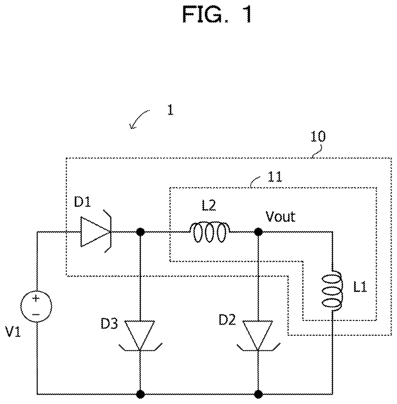
is a diagram illustrating an example of an oscillation circuit according to a first embodiment. An oscillation circuit 1 includes a diode D 1 (first diode), a diode D 2 (second diode), a diode D 3 (third diode), an inductor L 1 (first inductor), an inductor L 2 (second inductor), and a power supply unit V 1 (direct current (DC) DC power supply).
The diodes D 1 to D 3 are non-linear passive elements having negative differential resistances, and for example, an Esaki diode or a resonance tunnel diode is used.
In the oscillation circuit 1 , the diode D 1 having a first negative differential resistance and a composite inductor 11 are connected in series to form an oscillation unit 10 . In the composite inductor 11 , the inductors L 1 and L 2 are connected in series.
In addition, in the oscillation circuit 1 , the diode D 2 having a second negative differential resistance is connected to the inductor L 1 in parallel. Furthermore, the diode D 3 having a third negative differential resistance is connected to the diode D 1 in series and is connected to the composite inductor 11 in parallel. An output end of the oscillation circuit 1 is a common connection point (Vout) of the inductors L 1 and L 2 and the diode D 2 , and a burst pulse (neuron-like pulse) is output from the common connection point (Vout).
In a connection relationship of the components, a positive-side terminal of the power supply unit V 1 is connected to an anode of the diode D 1 , and a cathode of the diode D 1 is connected to an anode of the diode D 3 and one end of the inductor L 2 .
Another end of the inductor L 2 is connected to an anode of the diode D 2 and one end of the inductor L 1 . A negative-side terminal of the power supply unit V 1 is connected to another end of the inductor L 1 , a cathode of the diode D 2 , and a cathode of the diode D 3 .
is a diagram illustrating an example of the burst pulse. The vertical axis indicates a voltage (mV), the horizontal axis indicates time (μs). A burst pulse P as illustrated in is oscillated from the output end (common connection point) Vout of the oscillation circuit 1 illustrated in . The burst pulse P includes intermittent pulses P 1 and short pulses P 2 included in the intermittent pulse P 1 .
In this way, the oscillation circuit 1 oscillates the burst pulse using the components including the diodes D 1 to D 3 that are the non-linear elements having the negative differential resistances and the inductors L 1 and L 2 , with an application of a DC voltage. As a result, because it is possible to oscillate the burst pulse with a small number of components, it is possible to reduce a circuit size.
<Negative Differential Resistance>
Next, the negative differential resistance will be described. Note that, hereinafter, a diode having a negative differential resistance may be referred to as a tunnel diode. Therefore, the diodes D 1 to D 3 may be referred to as tunnel diodes D 1 to D 3 , respectively.
The tunnel diode has characteristics that a concentration of impurities doped in a p-type and an n-type layers is higher than a concentration of impurities of a pn-junction diode and a transistor having normal rectifying characteristics.
is a diagram for explaining the negative differential resistance. high-impurity-concentration pn-junction current-voltage characteristics (forward characteristics) are illustrated, the vertical axis indicates a current, and the horizontal axis indicates a voltage. In a general pn-junction diode, when a forward bias is applied (positive voltage is applied to p side, and negative voltage is applied to n side), a current increases with a voltage equal to or higher than a forward junction voltage.
In contrast, in a high-impurity-concentration pn-junction tunnel diode, when the forward bias is applied, a tunnel effect (phenomenon in which electrons pass through potential barrier created in depletion layer) is caused in a voltage range h 0 , and a current increases. Furthermore, when the forward bias is further increased, the tunnel effect is reduced in a voltage range hi, and characteristics that the current decreases as the voltage increases (negative differential resistance region) appear.
Since such characteristics correspond to that a differential resistance that is a ratio of a voltage increment and a current increment becomes negative, the characteristics are called a negative differential resistance (negative resistance) as a resistance component having a negative value. Furthermore, a slope of a characteristic curve in the negative differential resistance region can be expressed as a differential coefficient of the negative differential resistance.
By using such a voltage range (negative differential resistance region) in which the current decreases as the voltage increases for the tunnel diode, for example, a self-excited high-frequency oscillation circuit can be realized.
<Minimum Components of Oscillation Circuit>
Next, it will be described that the components included in the oscillation circuit 1 illustrated in are the minimum components (basic unit) used to oscillate a burst pulse, with reference to to 9 .
is a diagram illustrating an example of the oscillation circuit. An oscillation circuit 1 a 0 includes the tunnel diode D 1 , the inductor L 1 , and the power supply unit V 1 . A positive-side terminal of the power supply unit V 1 is connected to an anode of the tunnel diode D 1 , and a cathode of the tunnel diode D 1 is connected to one end of the inductor L 1 . A negative-side terminal of the power supply unit V 1 is connected to another end of the inductor L 1 .
is a diagram illustrating an example of an oscillation waveform. An oscillation pulse p 0 output from an output end Vout of the oscillation circuit 1 a 0 is illustrated. The vertical axis indicates a voltage (mV), and the horizontal axis indicates time (μs). The oscillation pulse p 0 is generated by using the single tunnel diode D 1 and the single inductor L 1 as in the oscillation circuit 1 a 0 .
A period of the oscillation pulse p 0 is about 15 μs, and a duty ratio of the pulse is about 50%. Furthermore, the oscillation pulse p 0 has a shorter repetition interval than that of the burst pulse in . Furthermore, due to non-linear characteristics of a current-voltage curve of the tunnel diode D 1 , a waveform of the oscillation pulse p 0 is not a sine wave and is a waveform with sharp rising and falling.
is a diagram illustrating an example of the oscillation circuit. An oscillation circuit 1 a 1 includes the tunnel diode D 1 , the tunnel diode D 2 , the inductor L 1 , and the power supply unit V 1 . A positive-side terminal of the power supply unit V 1 is connected to an anode of the tunnel diode D 1 , and a cathode of the tunnel diode D 1 is connected to an anode of the tunnel diode D 2 and one end of the inductor L 1 . A negative-side terminal of the power supply unit V 1 is connected to another end of the inductor L 1 and a cathode of the tunnel diode D 2 .
is a diagram illustrating an example of the oscillation waveform. An oscillation pulse p 1 output from an output end Vout of the oscillation circuit 1 a 1 is illustrated. The vertical axis indicates a voltage (mV), and the horizontal axis indicates time (μs). As in the oscillation circuit 1 a 1 , the oscillation pulse p 1 is generated by connecting the tunnel diode D 2 in parallel to the inductor L 1 and in series with the tunnel diode D 1 , with respect to the oscillation circuit 1 a 0 .
A period of the oscillation pulse p 1 is approximately the same as the oscillation pulse p 0 , and a duty ratio of the pulse is asymmetrical. This can be assumed that a bypass line is added to the oscillation circuit 1 a 0 by the tunnel diode D 2 and a negative differential resistance and non-linear characteristics of the tunnel diode D 2 cause pulse width modulation.
is a diagram illustrating an example of the oscillation circuit. An oscillation circuit 1 a 2 includes the tunnel diode D 1 , the tunnel diode D 2 , the inductor L 1 , the inductor L 2 , and the power supply unit V 1 . A positive-side terminal of the power supply unit V 1 is connected to an anode of the tunnel diode D 1 , and a cathode of the tunnel diode D 1 is connected to one end of the inductor L 2 .
Another end of the inductor L 2 is connected to an anode of the tunnel diode D 2 and one end of the inductor L 1 . A negative-side terminal of the power supply unit V 1 is connected to another end of the inductor L 1 and a cathode of the tunnel diode D 2 .
is a diagram illustrating an example of the oscillation waveform. An oscillation pulse p 2 output from an output end Vout of the oscillation circuit 1 a 2 is illustrated. The vertical axis indicates a voltage (mV), and the horizontal axis indicates time (μs). As in the oscillation circuit 1 a 2 , the oscillation pulse p 2 is generated by inserting the inductor L 2 between the cathode of the tunnel diode D 1 , the anode of the tunnel diode D 2 , and the one end of the inductor L 1 , with respect to the oscillation circuit 1 a 1 . The oscillation pulse p 2 has a waveform in which a short pulse train is superimposed on an intermittent pulse.
In this way, by configuring the oscillation circuit 1 a 2 by adding the inductor L 2 to the oscillation circuit 1 a 1 so as to form a connection configuration illustrated in , it is possible to generate a burst pulse in which short pulse trains are intermittently repeated.
Furthermore, the oscillation circuit 1 as illustrated in is configured by connecting the tunnel diode D 3 to the tunnel diode D 1 in series and to the composite inductor 11 including the inductors L 1 and L 2 in parallel, with respect to the oscillation circuit 1 a 2 .
By adding the tunnel diode D 3 to the oscillation circuit 1 a 2 , a negative differential resistance and non-linear characteristics of the tunnel diode D 3 enable to adjust an intermittent degree of the intermittent pulse (ratio of the number of intermittent pulses included in certain period) with respect to the oscillation pulse p 2 .
Note that an amplitude of the burst pulse can be changed by varying a size of the tunnel diode D 1 (size of element). A diode size is proportional to an amount of a current flowing in a diode. When the size of the tunnel diode D 1 increases, the amplitude of the burst pulse increases, and when the size of the tunnel diode D 1 decreases, the amplitude of the burst pulse decreases.
As described above, the oscillation circuit 1 using the minimum components including the tunnel diodes D 1 to D 3 and the inductors L 1 and L 2 can oscillate the burst pulse that imitates a neural signal pulse, and it is possible to reduce the circuit size.
<Characteristics of Tunnel Diode>
Next, characteristics of the tunnel diodes D 1 to D 3 will be described. is a diagram illustrating an example of characteristics of a negative differential resistance of a tunnel diode. The vertical axis indicates a current, and the horizontal axis indicates a voltage. Characteristic curves k 1 to k 5 indicate characteristics of negative differential resistances of tunnel diodes.
The characteristic curve k 1 indicates characteristics of a negative differential resistance of a tunnel diode with a size of 100 μm, the characteristic curve k 2 indicates characteristics of a negative differential resistance of a tunnel diode with a size of 80 μm, and the characteristic curve k 3 indicates characteristics of a negative differential resistance of a tunnel diode with a size of 60 μm.
Furthermore, the characteristic curve k 4 indicates characteristics of a negative differential resistance of a tunnel diode with a size of 20 μm, and the characteristic curve k 5 indicates characteristics of a negative differential resistance of a tunnel diode with a size of 10 μm. In this way, the current that flows differs according to the size of the tunnel diode, and the larger the size of the tunnel diode is, the larger the negative differential resistance is.
In the oscillation circuit 1 , by setting the negative differential resistance of the tunnel diode D 1 to have larger characteristics than the negative differential resistances of the tunnel diodes D 2 and D 3 , the tunnel diode D 1 is caused to function as an oscillation driving source of the oscillation circuit 1 .
Therefore, for the tunnel diode D 1 , for example, the size having the characteristics of one of the characteristic curves k 1 to k 3 is selected. Furthermore, for the tunnel diodes D 2 and D 3 , the size having the characteristics of one of the characteristic curves k 4 and k 5 is selected.
For example, the size of the tunnel diode D 1 is assumed as 100 μm (characteristic curve k 1 ), the size of the tunnel diode D 2 is assumed as 20 μm (characteristic curve k 4 ), and the size of the tunnel diode D 3 is assumed as 10 μm (characteristic curve k 5 ). Note that, as long as the negative differential resistances of the tunnel diodes D 2 and D 3 are smaller than the negative differential resistance of the tunnel diode D 1 , the negative differential resistances of the tunnel diodes D 2 and D 3 may be the same (sizes of tunnel diodes D 2 and D 3 may be the same).
By selecting the size of the tunnel diode in this way, the tunnel diode D 1 can be caused to function as the oscillation driving source of the oscillation circuit 1 , and in addition, the burst pulse can be stably oscillated from the tunnel diode D 1 and a composite series inductor including the inductors L 1 and L 2 .
Note that a plurality of tunnel diodes having different negative differential resistances can have the same configuration with respect to a semiconductor layer. Therefore, without performing integration from different types of wafers, it is possible to collectively configure the oscillation circuits 1 on a single wafer and, it is possible to construct an oscillation circuit group of the burst pulse.
<Characteristics of Composite Inductor>
Next, characteristics of the inductors L 1 and L 2 included in the composite inductor 11 will be described with reference to to 13 . to 13 are diagrams illustrating an example of a waveform of the burst pulse. The vertical axis indicates a voltage (mV), the horizontal axis indicates time (μs).
illustrates a waveform G 0 of a burst pulse when an inductance of the inductor L 1 (first inductance) and an inductance of the inductor L 2 (second inductance) are the same values (for example, L 1 =L 2 =100 pH).
illustrates a waveform G 1 of a burst pulse when the inductance of the inductor L 1 is a smaller value than the inductance of the inductor L 2 (for example, L 1 =50 pH, L 2 =100 pH).
By setting the inductance of the inductor L 1 to be smaller than the inductance of the inductor L 2 , a period of an intermittent pulse can be shorter than that of the waveform G 0 , and the number of short pulses included in the intermittent pulse can be smaller than that of the waveform G 0 .
illustrates a waveform G 2 of a burst pulse when the inductance of the inductor L 2 is a smaller value than the inductance of the inductor L 1 (for example, L 1 =100 pH, L 2 =50 pH).
By setting the inductance of the inductor L 2 to be smaller than the inductance of the inductor L 1 , a period of an intermittent pulse can be shorter than that of the waveform G 0 , and the number of short pulses included in the intermittent pulse can be larger than that of the waveform G 0 .
In this way, by changing setting of each inductance of the inductors L 1 and L 2 , it is possible to adjust the interval of the intermittent pulse period and to increase or decrease the number of short pulses to be superimposed in the intermittent pulse. Therefore, since the intermittent pulse period and the number of short pulses can be flexibly adjusted, it is possible to oscillate a burst pulse that is suitable for desired information processing.
Second Embodiment
Next, a second embodiment will be described. In the first embodiment described above, a DC power supply is used as an input power supply. However, in a second embodiment, an alternating current (AC) power supply or a power supply that outputs a voltage obtained by superimposing the AC voltage on the DC voltage (hereinafter, referred to as DC+AC voltage) is used to oscillate various burst pulses.
is a diagram illustrating an example of an oscillation circuit according to the second embodiment. An oscillation circuit 1 b includes tunnel diodes D 1 to D 3 , inductors L 1 and L 2 , and a power supply unit V 2 . The power supply unit V 2 is the AC power supply or the power supply that outputs the DC+AC voltage. Note that, since a configuration other than the power supply unit V 2 is the same as that in , description of a circuit configuration will be omitted.
is a diagram illustrating an example of a waveform of a burst pulse. The vertical axis indicates a voltage (mV), and the horizontal axis indicates time (ms). In the oscillation circuit 1 b , it is assumed that the power supply unit V 2 output the DC+AC voltage. A waveform g 11 is a waveform of the DC+AC voltage of the power supply unit V 2 , and a waveform g 12 indicates a waveform of a burst pulse output from an output end Vout of the oscillation circuit 1 b.
By inputting a power supply voltage to which a random AC voltage is applied, in addition to the DC voltage by the power supply unit V 2 , the waveform of the burst pulse can be complexly changed by varying the input voltage. Note that the random AC voltage is a voltage that changes an amplitude or a frequency of an AC voltage.
is a diagram illustrating an example of an oscillation circuit group including a plurality of oscillation circuits. An oscillation circuit group 1 B includes oscillation circuits 1 b 1 , 1 b 2 , to 1 bn . The oscillation circuits 1 b 1 , 1 b 2 , to 1 bn respectively include power supply units V 2 b - 1 , V 2 b - 2 , to V 2 b - n that output AC voltages different from each other. Characteristics of the tunnel diodes D 1 to D 3 and the inductors L 1 and L 2 are common in the oscillation circuits 1 b 1 , 1 b 2 , to 1 bn.
The oscillation circuit group 1 B with such a configuration can oscillate n burst pulses having waveforms different from each other, from output ends Vout of the oscillation circuits 1 b 1 , 1 b 2 , to 1 bn.
is a diagram illustrating an example of a waveform of the burst pulse. The vertical axis indicates a voltage (mV), the horizontal axis indicates time (μs). Graphs g1 to g9 illustrate waveforms of burst pulses output from the output ends Vout of the respective oscillation circuits 1 b 1 to 1 b 9 when a certain regularity is given to a change in the AC voltage output from the power supply unit.
In the example in , sine wave AC voltages with amplitudes different from each other are output from power supply units V 2 b - 1 to V 2 b - 9 . For example, a sine wave signal is changed from 500 mV to 450 mV (nine AC voltage signals) every amplitude of 50 mV.
Here, in the above, a configuration is used in which the plurality of AC power supplies that outputs AC voltages with amplitudes different from each other is provided. However, if only the amplitude of the AC voltage is changed, the power supply unit can include a single AC power supply and a plurality of resistors having resistance values different from each other.
is a diagram illustrating an example of a configuration of the power supply unit. This is an example of a power supply unit V 0 including a single AC power supply and a plurality of resistors. The power supply unit V 0 includes an AC power supply v 10 and resistors R 1 to Rn. An output end of the AC power supply v 10 is connected to one end of each of the resistors R 1 to Rn, and another ends of each of the resistors R 1 to Rn serve as input ends of n oscillation circuits. Each resistance value of each of the resistors R 1 to Rn is different.
In this way, a configuration is used in which the AC power supply v 10 that outputs a sine wave signal of an AC voltage is shared and a plurality of resistor elements having different resistance values branch and output the sine wave signal. As a result, it is possible to apply the AC voltages having the amplitudes different from each other to the n oscillation circuits. With such a configuration, it is possible to generate sine wave waveforms having the same period and different amplitudes as input signals with a circuit configuration having a smaller number of components.
Note that, in the above, it has been described that the characteristics of the tunnel diodes and the inductors in the oscillation circuits are set to be the same so as to vary the burst pulse waveform based on a fluctuation in an output voltage from the power supply unit. However, the characteristics of the tunnel diodes and the inductors may be changed for each oscillation circuit.
For example, by using an inductor having an inductance different for each oscillation circuit, it is possible to change a basic frequency of the burst pulse (frequency of intermittent pulse, frequency of short pulse) and to oscillate various burst pulses.
Furthermore, by using such an oscillation circuit, for example, for reservoir computing (reservoir computing) to be described later that is one of architectures of a recursive neural network, it is possible to improve a performance of reservoir computing.
Third Embodiment
Next, a third embodiment will be described. In the third embodiment, a feedback loop is provided in an oscillation circuit.
is a diagram illustrating an example of a configuration of the oscillation circuit including the feedback loop. An oscillation circuit 3 is a circuit that includes an oscillation circuit 1 (first oscillation circuit) and an oscillation circuit 2 (second oscillation circuit) and includes a feedback loop that uses an output signal of the oscillation circuit 1 as an input of the oscillation circuit 2 and an output signal of the oscillation circuit 2 as an input of the oscillation circuit 1 .
The oscillation circuit 1 includes a tunnel diode D 1 (first diode), a tunnel diode D 2 (second diode), a tunnel diode D 3 (third diode), an inductor L 1 (first inductor), an inductor L 2 (second inductor), a power supply unit V 1 a (first power supply unit), and a rectification diode d 1 (first rectification diode).
Furthermore, in the oscillation circuit 1 , the tunnel diode D 1 and a composite inductor 11 (first composite inductor) are connected in series so as to form an oscillation unit 10 (first oscillation unit). The composite inductor 11 is a composite series inductor that includes the inductors L 1 and L 2 connected in series.
The oscillation circuit 2 includes a tunnel diode D 11 (fourth diode), a tunnel diode D 12 (fifth diode), a tunnel diode D 13 (sixth diode), an inductor L 11 (third inductor), an inductor L 12 (fourth inductor), a power supply unit V 1 b (second power supply unit), and a rectification diode d 2 (second rectification diode).
In the oscillation circuit 2 , the tunnel diode D 11 and a composite inductor 21 (second composite inductor) are connected in series so as to form an oscillation unit 20 (second oscillation unit). The composite inductor 21 is a composite series inductor that includes the inductors L 11 and L 12 connected in series.
Here, in the oscillation circuit 3 , the normal rectification diodes d 1 and d 2 are provided, in order to prevent a power supply voltage component from flowing backward due to the feedback loop. Furthermore, each of the oscillation circuits 1 and 2 in the oscillation circuit 3 is a floating circuit (non-grounded circuit) and has a configuration in which interaction is taken only by the feedback loop.
Moreover, a feedback loop (first feedback loop) is formed in which an input end al (first input end) of the oscillation circuit 1 is connected to an output end Vout 2 (second output end) of the oscillation circuit 2 . Furthermore, a feedback loop (second feedback loop) is formed in which an input end b 1 (second input end) of the oscillation circuit 2 is connected to an output end Vout 1 (first output end) of the oscillation circuit 1 .
In a connection relationship of the components, a positive-side terminal (first output terminal) of the power supply unit V 1 a is connected to an anode of the tunnel diode D 1 and a cathode of the rectification diode d 2 . A cathode of the tunnel diode D 1 is connected to an anode of the tunnel diode D 3 and one end of the inductor L 2 .
Another end of the inductor L 2 is connected to an anode of the tunnel diode D 2 , an anode of the rectification diode d 1 , the output end Vout 1 , and one end of the inductor L 1 . A negative-side terminal (second output terminal) of the power supply unit V 1 a is connected to another end of the inductor L 1 , a cathode of the tunnel diode D 2 , and a cathode of the tunnel diode D 3 .
On the other hand, a positive-side terminal (third output terminal) of the power supply unit V 1 b is connected to an anode of the tunnel diode D 11 and a cathode of the rectification diode d 1 . A cathode of the tunnel diode D 11 is connected to an anode of the tunnel diode D 13 and one end of the inductor L 12 .
Another end of the inductor L 12 is connected to an anode of the tunnel diode D 12 , an anode of the rectification diode d 2 , the output end Vout 2 , and one end of the inductor L 11 . A negative-side terminal (fourth output terminal) of the power supply unit V 1 b is connected to another end of the inductor L 11 , a cathode of the tunnel diode D 12 , and a cathode of the tunnel diode D 13 .
is a diagram illustrating an example of the waveform of the burst pulse. The vertical axis indicates a voltage (mV), and the horizontal axis indicates time (ms). A graph g 21 illustrates a waveform of a burst pulse output from the output end Vout 1 , and a graph g 22 illustrates a waveform of a burst pulse output from the output end Vout 2 .
In this way, by providing the feedback loops in the two oscillation circuits 1 and 2 , the oscillation circuit 3 can generate complex and diverse burst pulse waveforms. Note that, in the above, a configuration has been described in which the two oscillation circuits are connected to each other. However, more oscillation circuits may be used. In that case, by unbalancing the number of interconnections, it is possible to generate more complex and diverse burst pulses.
Fourth Embodiment
Next, a fourth embodiment will be described. The fourth embodiment is an information processing device in which an oscillation circuit 1 is applied to reservoir computing. is a diagram illustrating an example of a reservoir circuit. A reservoir circuit 4 includes the plurality of oscillation circuits 1 and in which the oscillation circuits 1 are arranged in a two-dimensional grid pattern. Furthermore, feedback loops (arrow in figure) of the plurality of oscillation circuits 1 are randomly generated.
In this way, the plurality of oscillation circuits 1 connected to each other with the random feedback loops function as non-linear nodes in the reservoir circuit 4 . As a result, a more complex and high-performance reservoir computing function can be realized as compared with a case where one node includes simple non-linear elements (diode, inductor, or the like).
is a diagram illustrating an example of a reservoir computing device. A reservoir computing device 40 includes an input circuit 41 , the reservoir circuit 4 , a training data processing circuit 42 , and an output circuit 43 . Furthermore, in the output circuit 43 , a reading weighting unit 43 a is arranged.
Data is input from the input circuit 41 to the reservoir circuit 4 , and the reservoir circuit 4 executes arithmetic processing on the input data. At the time of reservoir training, the reading weighting unit 43 a adjusts a weighting value, based on an error between training data (teacher data) output from the training data processing circuit 42 and the data on which the arithmetic processing has been executed, and the adjusted data is output from the output circuit 43 . In this way, by adjusting the weighting based on the error between the output of the reservoir circuit 4 and the training data, it is possible to perform high-speed training in real time.
Fifth Embodiment
A fifth embodiment is an information processing device in which an oscillation circuit 1 is applied to a spiking neural network system. is a diagram illustrating an example of the spiking neural network system. A spiking neural network system 5 includes oscillation circuits 1 - 1 to 1 - 4 , encoders 51 - 1 to 51 - 4 , a neural network unit 52 including a plurality of neuron elements connected like a network.
The oscillation circuits 1 - 1 to 1 - 4 oscillate burst pulses. The encoders 51 - 1 to 51 - 4 receive burst pulses and input signals, mix the burst pulses and the input signals, generate encoded pulse signals, and output the signals to the neural network unit 52 . Note that the encoders 51 - 1 to 51 - 4 modulate the input signal based on at least any one of an intensity, a frequency, and an interval of the burst pulse and generate the encoded pulse signals. The neural network unit 52 executes information processing based on the encoded pulse signal.
As described above, according to the oscillation circuit of the present invention, the circuit including the tunnel diode having the negative differential resistance in a predetermined voltage range and the inductor is used as a basic unit so as to oscillate the burst pulse. As a result, it is possible to configure a low-power highly-integrated circuit that has a small number of components and oscillates neuron-like burst pulses.
The embodiments have been exemplified above, and the configuration of each unit described in the embodiments may be replaced with another configuration having a similar function. Furthermore, any other components and steps may be added. Moreover, any two or more configurations (features) of the embodiments described above may be combined.
The above description merely indicates the principle of the present invention. Moreover, numerous modifications and changes can be made by those skilled in the art. The present invention is not limited to the exact configuration and application examples illustrated and described above, and all corresponding modifications and equivalents are regarded within the scope of the present invention by appended claims and equivalents thereof.
All examples and conditional language provided herein are intended for the pedagogical purposes of aiding the reader in understanding the invention and the concepts contributed by the inventor to further the art, and are not to be construed as limitations to such specifically recited examples and conditions, nor does the organization of such examples in the specification relate to a showing of the superiority and inferiority of the invention. Although one or more embodiments of the present invention have been described in detail, it should be understood that the various changes, substitutions, and alterations could be made hereto without departing from the spirit and scope of the invention.
Figures (20)
Citations
This patent cites (10)
- US3225317
- US5014018
- US20050146386
- US20120068778
- US20140098845
- USH01-272201
- US2005-018500
- US2005-333227
- US2014-517620
- US2012/163403