Power Supply Apparatus for Stabilizing Power Supply Capability of Auxiliary Winding Provided in Transformer
Abstract
A protection circuit protects a rectifier circuit from an inrush current inputted to a smoothing circuit. A short-circuiting circuit does not short the protection circuit while an inrush current may occur, and shorts it while an inrush current does not occur. A transformer has a primary winding, a secondary winding and an auxiliary winding. A delay circuit delays a timing at which an operation of a load connected to the auxiliary winding is started with respect to a timing at which an operation of the short-circuiting circuit is started. A rectifying and smoothing circuit generates an output voltage by rectifying and smoothing the secondary side voltage. The short-circuiting circuit is driven by the output voltage.
Claims (17)
1. A power supply apparatus comprising: a rectifier circuit configured to rectify alternating current inputted from an alternating power supply; a smoothing circuit configured to smooth output of the rectifier circuit: a protection circuit configured to protect the rectifier circuit from an inrush current inputted to the smoothing circuit; a short-circuiting circuit configured to not short circuit the protection circuit in a period in which an inrush current may occur, and configured to short circuit the protection circuit in a period in which an inrush current does not occur; a transformer having a primary winding to which a primary side voltage generated by the smoothing circuit is applied, a secondary winding for generating a secondary side voltage corresponding to a predetermined winding ratio, and an auxiliary winding magnetically coupled to the primary winding; a delay circuit configured to delay a timing at which an operation of a load connected to the auxiliary winding is started with respect to an operation of a timing at which the short-circuiting circuit is started; a switching element configured to switch a current that flows through the primary winding so that the secondary side voltage becomes a target voltage; and a rectifying and smoothing circuit configured to generate an output voltage by rectifying and smoothing the secondary side voltage, wherein the short-circuiting circuit is driven by the output voltage.
14. An image forming apparatus comprising: a power supply apparatus; and an image forming unit configured to operate by being supplied with an output voltage from the power supply apparatus, and form an image on a recording medium, wherein the power supply apparatus comprises: a rectifier circuit configured to rectify alternating current inputted from an alternating power supply; a smoothing circuit configured to smooth output of the rectifier circuit: a protection circuit configured to protect the rectifier circuit from an inrush current inputted to the smoothing circuit; a short-circuiting circuit configured to not short circuit the protection circuit in a period in which an inrush current may occur, and configured to short circuit the protection circuit in a period in which an inrush current does not occur; a transformer having a primary winding to which a primary side voltage generated by a smoothing circuit is applied, a secondary winding for generating a secondary side voltage corresponding to a predetermined winding ratio, and an auxiliary winding magnetically coupled to the primary winding; a delay circuit configured to delay a timing at which an operation of a load connected to the auxiliary winding is started with respect to an operation of a timing at which the short-circuiting circuit is started; a switching element configured to switch a current that flows through the primary winding so that the secondary side voltage becomes a target voltage; and a rectifying and smoothing circuit configured to generate an output voltage by rectifying and smoothing the secondary side voltage, wherein the short-circuiting circuit is driven by the output voltage.
15. A power supply apparatus comprising: a rectifier circuit configured to rectify alternating current inputted from an alternating power supply; a smoothing circuit configured to smooth output of the rectifier circuit: a transformer having a primary winding to which a primary side voltage generated by the smoothing circuit is applied, a secondary winding for generating a secondary side voltage corresponding to a predetermined winding ratio, and an auxiliary winding magnetically coupled to the primary winding; a switching element configured to switch a current that flows through the primary winding so that the secondary side voltage becomes a target voltage; a rectifying and smoothing circuit configured to generate an output voltage by rectifying and smoothing the secondary side voltage; and a relay, provided on a primary side of the transformer and configured to be driven by the output voltage, and which becomes a part of a load of a secondary side of the transformer, wherein in a case where the relay becomes on by the output voltage being used as a voltage for turning the relay on, the load of the secondary side of the transformer increases, and a power supply capability of the auxiliary winding increases thereby.
Show 14 dependent claims
2. The power supply apparatus according to claim 1 , further comprising: a control circuit configured to not supply an output voltage to the short-circuiting circuit in a period in which the inrush current may occur, and configured to supply the output voltage to the short-circuiting circuit in a period in which the inrush current does not occur.
3. The power supply apparatus according to claim 2 , further comprising: a first switch configured to switch whether to supply the output voltage to the protection circuit in accordance with a signal outputted from the control circuit, wherein the control circuit is configured to, when an operation of the short-circuiting circuit is started by the output voltage being supplied to the short-circuiting circuit, start output of the signal, and the first switch is configured to switch from OFF to ON based on the signal and supply the output voltage to the protection circuit.
4. The power supply apparatus according to claim 3 , wherein the signal is also used as a signal to start up the load that operates by providing electric power generated by the auxiliary winding.
5. The power supply apparatus according to claim 4 , further comprising: a second switch configured to operate so as to supply electric power generated by the auxiliary winding to the load when the signal is inputted.
6. The power supply apparatus according to claim 5 , wherein the delay circuit is configured to, by delaying a timing at which the signal is inputted to the second switch with respect to a timing at which the signal is inputted to the first switch, delay a timing at which the operation of the load is started with respect to a timing at which the operation of the short-circuiting circuit is started.
7. The power supply apparatus according to claim 6 , further comprising: a photocoupler provided between the control circuit and the second switch, wherein the photocoupler insulates a circuit group provided on a primary side of the transformer from a circuit group provided on a secondary side of the transformer, wherein the delay circuit is provided between the control circuit and the photocoupler, or between the photocoupler and the second switch.
8. The power supply apparatus according to claim 1 , wherein a load connected to the auxiliary winding includes a controller that controls the switching element to maintain the secondary side voltage at the target voltage.
9. The power supply apparatus according to claim 2 , further comprising: a generation circuit configured to generate a load voltage supplied to the load based on electric power generated in the auxiliary winding, wherein the delay circuit further comprises a circuit that delays a timing at which the operation of the load is started with respect to a timing at which the operation of the short-circuiting circuit is started by delaying a timing at which the load voltage is supplied to the load.
10. The power supply apparatus according to claim 1 , further comprising: a power factor correction circuit connected to a primary side of the transformer, wherein the load connected to the auxiliary winding includes a controller that controls the power factor correction circuit.
11. The power supply apparatus according to claim 10 , wherein: the delay circuit is further configured to delay a timing at which the operation of the power factor correction circuit is started with respect to a timing at which the operation of the short-circuiting circuit is started.
12. The power supply apparatus according to claim 11 , further comprising: a generation circuit configured to generate an operation voltage for the power factor correction circuit based on electric power generated in the auxiliary winding, wherein the delay circuit is configured to delay a timing at which the operation of the power factor correction circuit is started with respect to a timing at which the operation of the short-circuiting circuit is started by delaying a timing at which the operation voltage is supplied to the power factor correction circuit.
13. The power supply apparatus according to claim 1 , wherein the protection circuit has a resistance element for decreasing the inrush current, the short-circuiting circuit has a relay connected in parallel to the resistance element, and the relay configured to not short circuit the resistance element in a period in which an inrush current may occur, and configured to short circuit the resistance element in a period in which an inrush current does not occur.
16. The power supply apparatus according to claim 15 , wherein by the relay becoming on, a coil arranged in the relay becomes a part of the load of the secondary side of the transformer.
17. The power supply apparatus according to claim 15 , wherein the relay is connected in series to one end of the primary winding of the transformer.
Full Description
Show full text →
BACKGROUND OF THE INVENTION
Field of the Invention
The present invention relates to a power supply apparatus for stabilizing a power supply capability of an auxiliary winding provided in a transformer.
Description of the Related Art
Generally, a power supply apparatus converts an input voltage to an output voltage by a transformer. There are also transformers with an auxiliary winding, in addition to a primary winding and secondary winding, among the transformers used in power supply apparatuses. Electric power generated by the auxiliary winding may be used to drive a load arranged on a primary side of the transformer (Japanese Patent Laid-Open No. 11-0032480 and US-2018-0358889).
The power supply capability of the auxiliary winding is proportional to the magnitude of the load connected to the secondary side of the transformer. Therefore, when a secondary side load is light, the power supply capability of the auxiliary winding is insufficient, and it is impossible to stably drive the primary side load connected to the auxiliary winding. To artificially increase the secondary side load, it is conceivable to provide a dummy resistor (bleeder resistor) in parallel to the secondary side load. However, this will likely introduce an increase in the number of parts and an increase in the cost of the power supply apparatus.
SUMMARY OF THE INVENTION
The present invention provides a power supply apparatus comprising the following elements. A rectifier circuit is configured to rectify alternating current inputted from an alternating power supply. A smoothing circuit is configured to smooth output of the rectifier circuit. A protection circuit is configured to protect the rectifier circuit from an inrush current inputted to the smoothing circuit. A short-circuiting circuit is configured to not short circuit the protection circuit in a period in which an inrush current may occur, and configured to short circuit the protection circuit in a period in which an inrush current does not occur. A transformer has a primary winding to which a primary side voltage generated by the smoothing circuit is applied, a secondary winding for generating a secondary side voltage corresponding to a predetermined winding ratio, and an auxiliary winding magnetically coupled to the primary winding. A delay circuit configured to delay a timing at which an operation of a load connected to the auxiliary winding is started with respect to an operation of a timing at which the short-circuiting circuit is started. A switching element is configured to switch a current that flows through the primary winding so that the secondary side voltage becomes a target voltage. A rectifying and smoothing circuit is configured to generate an output voltage by rectifying and smoothing the secondary side voltage. The short-circuiting circuit is driven by the output voltage.
Further features of the present invention will become apparent from the following description of exemplary embodiments (with reference to the attached drawings).
BRIEF DESCRIPTION OF THE DRAWINGS
is a circuit diagram of a power supply apparatus.
is a timing chart illustrating voltage and signal change.
is a circuit diagram of a power supply apparatus.
is a timing chart illustrating voltage and signal change.
is a circuit diagram of a power supply apparatus.
is a timing chart illustrating voltage and signal change.
is a schematic diagram of an image forming apparatus.
DESCRIPTION OF THE EMBODIMENTS
Hereinafter, embodiments will be described in detail with reference to the attached drawings. Note, the following embodiments are not intended to limit the scope of the claimed invention. Multiple features are described in the embodiments, but limitation is not made to an invention that requires all such features, and multiple such features may be combined as appropriate. Furthermore, in the attached drawings, the same reference numerals are given to the same or similar configurations, and redundant description thereof is omitted.
First Embodiment
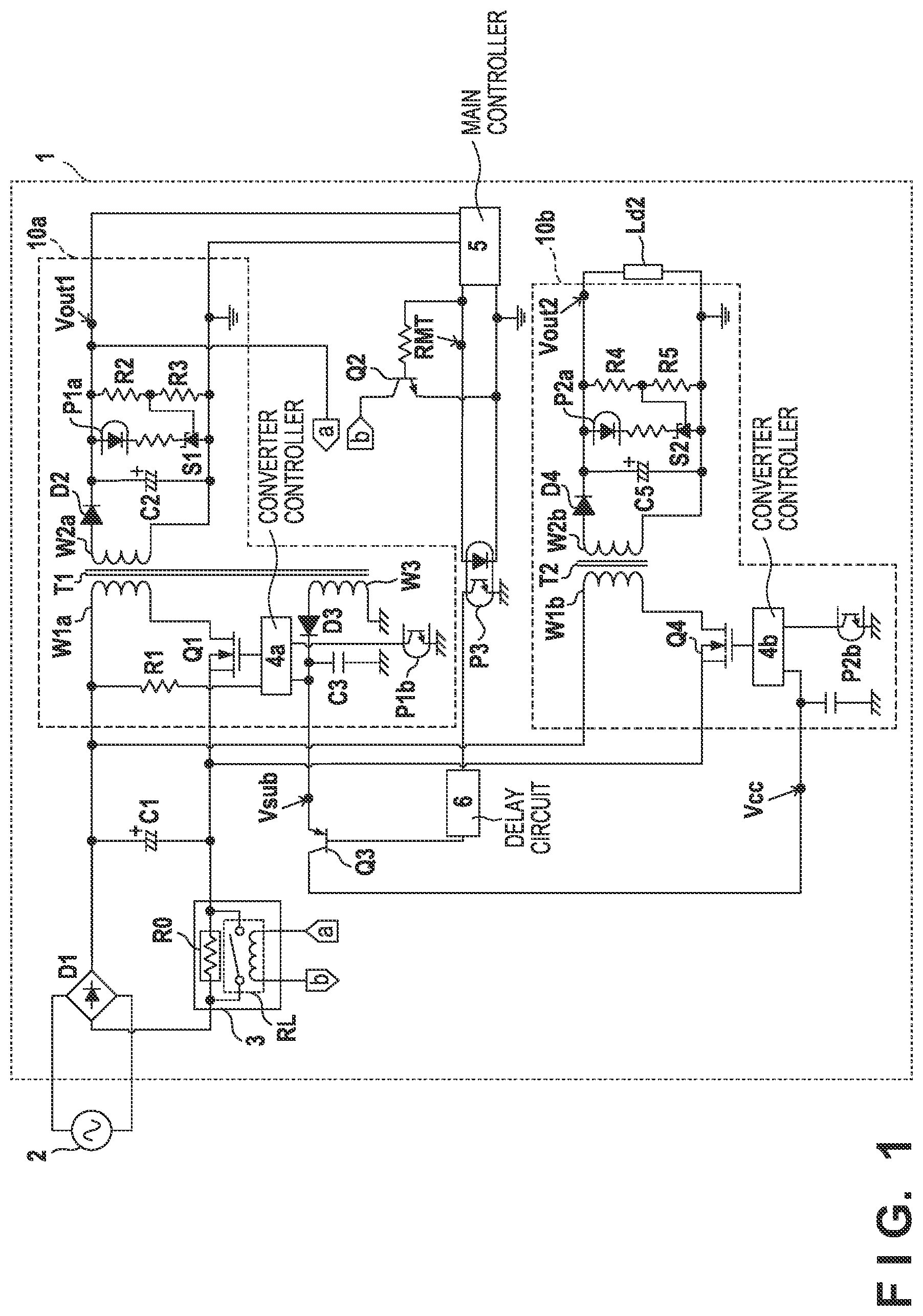
As shown in , a power supply apparatus 1 is an AC/DC converter for converting an alternating current voltage supplied from a commercial power supply 2 to a direct current voltage and outputting the result. The power supply apparatus 1 includes a first converter 10 a and a second converter 10 b . The power supply apparatus 1 may be employed, for example, as a power supply for supplying electric power to an image forming apparatus. An electric device such as an image forming apparatus has a normal power mode in which power consumption is large as in a state in which the device is operating, and a power saving mode in which the device is not operating and a part of the power supply is stopped and the power consumption is smaller than that in the normal power mode. Therefore, the first converter 10 a may function as a sub power supply that operates in both power modes. The second converter 10 b may be stopped in the power saving mode and function as a main power supply that operates in the normal power mode. Therefore, the first converter 10 a always operates when the power supply apparatus 1 is connected to the commercial power supply 2 , and supplies electric power to a main controller 5 which is for controlling an electric device. When the electric device is in the power saving mode, the second converter 10 b is stopped. When the electric device is operating in the normal power mode, the second converter 10 b receives a signal from the main controller 5 to start operation and supply the necessary electric power to the electric device.
AC/DC Converter
The power supply apparatus 1 has an AC/DC converter that converts an alternating current voltage to a direct current voltage. A diode bridge D 1 provided in the AC/DC converter functions as a rectifier circuit (rectifier or rectifier element) for rectifying the alternating current. A capacitor C 1 is an electrolytic capacitor or the like, and functions as a smoothing circuit (smoothing element) for smoothing the output current (pulsating current) of the diode bridge D 1 . By the pulsating current flowing into the capacitor C 1 , the capacitor C 1 is charged. When the alternating current voltage is inputted to the power supply apparatus 1 in a state where the end-to-end voltage across the capacitor C 1 is low, a large current (inrush current) can flow from the commercial power supply 2 to the capacitor C 1 . Therefore, a current limiting element R 0 is provided between the diode bridge D 1 and the capacitor C 1 . A large current (inrush current) flowing into the capacitor C 1 is limited by the current limiting element R 0 . Thus, a fuse (not shown) provided on the diode bridge D 1 and its front stage is protected. The current limiting element R 0 , for example, may be a resistance element or a thermistor.
Incidentally, the current limiting element R 0 functions at least in a period in which an inrush current is likely to occur, such as a period immediately after alternating current voltage is inputted to the power supply apparatus 1 (charging period of the capacitor C 1 ). However, in the period in which the inrush current will not occur, since the current limiting element R 0 consumes electric power, the efficiency of the power supply apparatus 1 is reduced. Therefore, in the period in which the inrush current is not generated, a relay RL short circuits the current limiting element R 0 . The current limiting element R 0 (protection circuit) and the relay RL (a short-circuiting circuit) forms an inrush current reduction circuit 3 .
First Converter
To the subsequent stage of the capacitor C 1 , the first converter 10 a and the second converter 10 b are connected. The first converter 10 a is a DC/DC converter.
In the first converter 10 a , the direct current voltage generated by the diode bridge D 1 and the capacitor C 1 is supplied to a converter controller 4 a through a start-up resistor R 1 . The converter controller 4 a is a control circuit for controlling an output voltage Vout 1 of the first converter 10 a to a target voltage.
One end of the capacitor C 1 is connected to one end of a primary winding W 1 a of a transformer T 1 . The other end of the capacitor C 1 is connected to the source of a switching element Q 1 (FET). The drain of the switching element Q 1 is connected to the other end of the primary winding W 1 a . The gate of the switching element Q 1 is connected to the converter controller 4 a . The converter controller 4 a , which is started up by charging the capacitor C 1 with a predetermined voltage, starts outputting a switching signal to the gate of the switching element Q 1 . By switching the input voltage applied to the primary winding W 1 a by the switching element Q 1 , an alternating current flows through the primary winding W 1 a . By this alternating current, an alternating current voltage corresponding to the winding ratio of the transformer T 1 is generated in a secondary winding W 2 a . A diode D 2 and a capacitor C 2 are disposed on the secondary side of the first converter 10 a . The diode D 2 functions as a rectifier circuit that rectifies the alternating current generated in the secondary winding W 2 a to generate a pulsating current. The capacitor C 2 smoothes the pulsating current output from the diode D 2 to generate a direct current. The end-to-end voltage across the capacitor C 2 is the output voltage Vout 1 of the first converter 10 a.
Resistors R 2 , R 3 , shunt regulator S 1 and a photocoupler form a feedback circuit that feeds back the output voltage Vout 1 to the converter controller 4 a . The photocoupler is configured by a light emitting diode P 1 a and a phototransistor P 1 b , and insulates the primary side and the secondary side of the first converter 10 a (the transformer T 1 ). Resistors R 2 and R 3 divide the output voltage Vout 1 , and form a voltage-dividing circuit for generating a detected voltage proportional to the output voltage Vout 1 . The detected voltage is inputted to the shunt regulator S 1 . When the detected voltage is higher than the reference voltage, the shunt regulator S 1 increases the current flowing through the light emitting diode P 1 a . However, when the detected voltage is lower than the reference voltage, the shunt regulator S 1 decreases the current flowing through the light emitting diode P 1 a . When a current flows through the light emitting diode P 1 a , the light emitting diode P 1 a emits light. A current corresponding to the amount of light of the light emitting diode P 1 a flows through the phototransistor P 1 b . Thus the output voltage Vout 1 of the first converter 10 a is fed back to the converter controller 4 a via a photocoupler. The converter controller 4 a controls a duty ratio of the switching signal supplied to the switching element Q 1 so that the output voltage Vout 1 of the first converter 10 a becomes the target voltage. The switching element Q 1 may be, for example, a MOSFET. If the output voltage Vout 1 of the first converter 10 a is lower than the target voltage, more electric power needs to be supplied to the secondary side of the transformer T 1 . Therefore, the converter controller 4 a increases the period during which the switching element Q 1 is turned on, and the current flowing through the primary winding W 1 a of the transformer T 1 increases. An auxiliary winding W 3 is wound around the same core as the primary winding W 1 a and the secondary winding W 2 a of the transformer. Voltage is also generated in the auxiliary winding W 3 at the same time the switching of the switching element Q 1 is started. Current flows through a diode D 3 by this voltage, and a capacitor C 3 is charged. In other words, a direct current voltage is generated at both ends of the capacitor C 3 . The power supply source across the capacitor C 3 serves as an end-to-end voltage for the converter controller 4 a . When adequate direct current voltage is provided from the capacitor C 3 to the converter controller 4 a , the converter controller 4 a disconnects the electric power that had been supplied through the start-up resistor R 1 . Thus, since no current flows in the start-up resistor R 1 , power consumption reduction is achieved.
Electric power generated by the auxiliary winding W 3 is also supplied to a converter controller 4 b of the second converter 10 b via a switch Q 3 . When the electric device operates in the normal power mode, the main controller 5 outputs an ON signal to the switch Q 3 via a photocoupler P 3 . The switch Q 3 may be a semiconductor switch such as a transistor.
When the switch Q 3 is turned from OFF to ON, the voltage Vsub generated by the auxiliary winding W 3 , the diode D 3 and the capacitor C 3 as the power supply voltage Vcc, is supplied to the converter controller 4 b . Thus, switching of a switching element Q 4 is started, and an output voltage Vout 2 is generated on the secondary side of the second converter 10 b.
The ON signal output by the main controller 5 further switches a switch Q 2 from OFF to ON. Thus, the output voltage Vout 1 is applied to the relay RL, the current limiting element R 0 is short circuited. The switch Q 2 may be a semiconductor switch such as a transistor.
Second Converter
The second converter 10 b is a DC/DC converter for converting the direct current voltage generated by the capacitor C 1 to the output voltage Vout 2 . The converter controller 4 b is a control circuit for controlling the output voltage Vout 2 of the second converter 10 b to a target voltage.
One end of the capacitor C 1 is connected to one end of a primary winding W 1 b of a transformer T 2 of the second converter 10 b . The other end of the capacitor C 1 is connected to the source of the switching element Q 4 of the second converter 10 b . The drain of the switching element Q 4 is connected to the other end of the primary winding W 1 b . The gate of the switching element Q 4 is connected to the converter controller 4 b . The converter controller 4 b started up by the completion of charging the capacitor C 3 and the main controller 5 outputting the on signal starts outputting a switching signal to the gate of the switching element Q 4 . By switching the input voltage applied to a primary winding W 1 b by the switching element Q 4 , an alternating current flows through the primary winding W 1 b . By this alternating current, an alternating current voltage corresponding to the winding ratio of a transformer T 2 is generated in a secondary winding W 2 b . A diode D 4 and a capacitor C 5 are disposed on the secondary side of the second converter 10 b . The diode D 4 functions as a rectifier circuit that rectifies the alternating current generated in the secondary winding W 2 b to generate a pulsating current. The capacitor C 5 smoothes the pulsating current output from the diode D 4 to generate a direct current. The end-to-end voltage across the capacitor C 5 is the output voltage Vout 2 of the second converter 10 b.
Resistors R 4 , R 5 , shunt regulator S 2 and a photocoupler form a feedback circuit that feeds back the output voltage Vout 2 to the converter controller 4 b . The photocoupler is configured by a light emitting diode P 2 a and a phototransistor P 2 b , and insulates the primary side and the secondary side of the second converter 10 b . Resistors R 4 and R 5 divide the output voltage Vout 2 , and form a voltage-dividing circuit for generating a detected voltage proportional to the output voltage Vout 2 . When the detected voltage is higher than the reference voltage, the shunt regulator S 2 increases the current flowing through the light emitting diode P 2 a . However, when the detected voltage is lower than the reference voltage, the shunt regulator S 2 decreases the current flowing through the light emitting diode P 2 a . When a current flows through the light emitting diode P 2 a , the light emitting diode P 2 a emits light. A current corresponding to the amount of light of the light emitting diode P 2 a flows through the phototransistor P 2 b . Thus the output voltage Vout 2 of the second converter 10 b is fed back to the converter controller 4 b via a photocoupler. The converter controller 4 b controls a duty ratio of the switching signal supplied to the switching element Q 4 so that the output voltage Vout 2 of the second converter 10 b becomes the target voltage. If the output voltage Vout 2 of the second converter 10 b is lower than the target voltage, more electric power needs to be supplied to the secondary side of the transformer T 2 . Therefore, the period during which the switching element Q 4 is turned on is increased, and the current flowing through the primary winding W 2 b of the transformer T 2 increases. A load Ld 2 is connected to the second converter 10 b.
Increase in the Secondary Side Load of the First Converter 10 a and the Function of a Delay Circuit 6
As a characteristic of a transformer, the load arranged on the secondary side of the first converter 10 a and the power supply capability of the auxiliary winding W 3 are proportional. If the secondary side load is light, the duty ratio of the switching element Q 1 required to maintain the output voltage Vout 1 becomes small. Therefore, it is harder for electric power to be supplied to the auxiliary winding W 3 . If the secondary side load of the first converter 10 a is light, the power supply capability of the auxiliary winding W 3 is insufficient, the second converter 10 b cannot operate, or may repeatedly start up and stop. Therefore, in the first embodiment, in order to increase the secondary side load of the first converter 10 a , the relay RL of the inrush current reduction circuit 3 is driven by the output voltage Vout 1 . This increases the power supply capability of the auxiliary winding W 3 . Also, in order to more stably operate the second converter 10 b , the operation start timing of the converter controller 4 b may be delayed by the delay circuit 6 .
Details of the power supply apparatus 1 of the first embodiment will be described with reference to a timing chart of . In , RMT is an ON signal of the switch Q 3 (Q 2 ) described above, and may be referred to herein as the operation start signal. Vsub is the voltage generated by the auxiliary winding W 3 . Vcc is the power supply voltage of the converter controller 4 b . Vout 2 is the output voltage of the second converter 10 b.
At time t 0 , the commercial power supply 2 is already inputting an alternating current voltage to the power supply apparatus 1 . Therefore, the first converter 10 a outputs the output voltage Vout 1 . However, the electric device, which is the load Ld 2 of the second converter 10 b , is operating in the power saving mode. Therefore, the second converter 10 b is stopped. Relay RL is also stopped (disconnected) to improve the standby power in the power saving mode. When the electric device is in the power saving mode, the input current to the power supply apparatus 1 is low. Therefore, less electric power is consumed by the current limiting element R 0 . Considering the electric power consumed by the relay RL, the standby power can be improved by disconnecting the relay RL when the electric device is in the power saving mode. This is because the electric power consumed by the relay RL may be more than the electric power consumed by the current limiting element R 0 . Therefore, the relay RL is disconnected in the power saving mode. When the electric device transitions from the power saving mode to the normal power mode, the second converter 10 b starts to operate. At this time, the electric power consumed by the relay RL becomes less than the electric power consumed by the current limiting element R 0 . In order to reduce loss at the current limiting element R 0 , the relay RL is electrically connected. Therefore, an external signal for switching the operation and stoppage of the second converter 10 b , and an external signal for switching the electrical connection and disconnection of the relay RL can both be by the same signal.
At time t 1 , the electric device starts transition into the normal power mode. The main controller 5 outputs an ON signal (operation start signal RMT) to start the operation to the second converter 10 b . In parallel to this, since the ON signal switches the switch Q 2 to ON, the output voltage Vout 1 turns the relay RL to ON. By the output voltage Vout 1 driving the relay RL, the secondary side load of the first converter 10 a is increased. For example, the power consumed by the secondary side is increased by about 0.5 W. As previously described, the output voltage Vout 1 of the first converter 10 a is fed back to the converter controller 4 a . Therefore, when the secondary side load is increased, the duty ratio of the switching element Q 1 is increased, and the output voltage Vout 1 is maintained at the target voltage. When the duty ratio of the switching element Q 1 increases, the electric power supplied to the secondary winding W 2 a of the transformer T 1 increases, and the electric power supplied to the auxiliary winding W 3 also increases. The voltage of the auxiliary winding W 3 is in the uncontrolled state. Therefore, in a state where the load of the auxiliary winding W 3 is constant, the voltage of the auxiliary winding W 3 increases in proportion to the secondary side load.
Power supply voltage Vcc is supplied to the converter controller 4 b at time t 2 . That is, at time t 1 , the ON signal (operation start signal RMT) is being output, but the timing at which the power supply voltage Vcc is supplied to the converter controller 4 b is time t 2 . This is because the delay circuit 6 delays the operation start signal RMT. Here, although the operation start signal RMT input to the switch Q 3 is delayed, the enable signal input from the main controller 5 or the like to the converter controller 4 b may be delayed by the delay circuit 6 .
As shown in , at time t 2 as compared with time t 1 , the power supply capability of the auxiliary winding W 3 is increased. This is because the relay RL is driven by the output voltage Vout 1 . As a result, from the time t 2 , it is possible to stably operate the second converter 10 b.
Thus, by using the relay RL to increase the secondary side load of the first converter 10 a , the need to provide a dummy resistor or the like on the secondary side of the transformer T 1 is reduced. The time required to operate the relay RL is, for example, about several tens of milliseconds. Therefore, the delay of the startup time of the second converter 10 b does not affect the operation of the device comprising the power supply apparatus 1 .
The delay circuit 6 is a circuit for delaying output of an inputted signal. The delay time brought on by the delay circuit 6 is preset so that the second converter 10 b starts operating after the relay RL starts operating.
The power supply apparatus 1 of the first embodiment includes the first converter 10 a and the second converter 10 b . However, the number of converters provided in the power supply apparatus 1 may be three or more. Electric power may also be supplied from the auxiliary winding W 3 to two or more converter controllers. In any case, it is sufficient that the relay RL is driven at the output voltage Vout 1 of the first converter 10 a at time t 1 . Further, the delay circuit 6 is provided so that electric power is supplied to the two or more converter controllers from the auxiliary winding W 3 at time t 2 .
In the first embodiment, an image forming apparatus was referred to as an example of an electric device, but the electric device is not limited thereto. Although the delay circuit 6 in is provided on the primary side of the power supply apparatus 1 may be provided on the secondary side. For example, the delay circuit 6 may be provided between the main controller 5 and the photocoupler P 3 .
Second Embodiment
In the first embodiment, in order to operate the second converter 10 b , the operation start signal RMT is an external signal from the main controller 5 was required. In the second embodiment, the operation start signal RMT for operating the second converter 10 b is omitted. Incidentally, the first converter 10 a need not be a sub power supply. The second converter 10 b need not be a main power supply.
shows the power supply apparatus 1 of the second embodiment. Of the circuit configuration shown in , the same reference numerals are given to the circuit configuration already described in , and the description thereof is omitted.
As shown in , a load Ld 1 is connected to the first converter 10 a . Further, in the power supply apparatus 1 , the main controller 5 and the photocoupler P 3 are not provided. Further, to the relay RL, the output voltage Vout 1 is supplied directly. That is, the load Ld 1 and the relay RL are connected in parallel to the first converter 10 a . Furthermore, the switches Q 2 and Q 3 are also omitted in the power supply apparatus 1 . The delay circuit 6 is disposed in the supply path of the voltage Vsub. That is, the delay circuit 6 directly delays the supply of the voltage Vsub.
In , instead of the operation start signal RMT, the output voltage Vout 1 is shown. At time t 0 , an alternating current voltage is inputted from the commercial power supply 2 to the power supply apparatus 1 . Thereby, the capacitor C 1 is charged. When the capacitor C 1 is charged to a predetermined voltage, the first converter 10 a starts operating. After the first converter 10 a starts operation, the current limiting element R 0 is not necessary. This is because when the charging of the capacitor C 1 is completed, the inrush current does not flow to the capacitor C 1 . Therefore, the relay RL is short circuited in order to reduce the electric power loss at the current limiting element R 0 . Specifically, when the first converter 10 a starts outputting the output voltage Vout 1 , the output voltage Vout 1 is applied to the relay RL, the relay RL is turned on (a short circuit state (conductive state)). Since current bypasses the current limiting element R 0 , and flows through the relay RL, the current limiting element R 0 ceases to consume electric power. In order to maintain the short circuit state of the relay RL, the output voltage Vout 1 must continue to be applied to the relay RL. That is, the relay RL increases the load of the first converter 10 a . Thereby, the power supply capability of the auxiliary winding W 3 increases.
The power supply voltage Vcc is supplied to the converter controller 4 b at time t 2 . Power supply voltage Vcc is a voltage generated by delaying the voltage Vsub by the delay circuit 6 . At time t 2 , the relay RL increases the power supply capability from the auxiliary winding W 3 . Therefore, the second converter 10 b operates stably by the power supply voltage Vcc. Thus, a relay RL is used to increase the secondary side load of the first converter 10 a . Therefore, it is possible to increase the power supply capability of the auxiliary winding W 3 without providing a dummy resistor on the secondary side.
Third Embodiment
In the first embodiment and the second embodiment, the load of the auxiliary winding W 3 was the converter controllers 4 a and 4 b . As shown in , a PFC controller 51 is used as a load of the auxiliary winding W 3 in the third embodiment. In the third embodiment, the same reference numerals are assigned to the same items as those in the first and second embodiments, and a description thereof is omitted.
A PFC circuit 50 is a power factor correction circuit. A capacitor C 6 for rectifying the pulsating current output from the diode bridge D 1 is provided in the front stage of the PFC circuit 50 . The PFC circuit 50 has a booster circuit composed of a coil L 1 , a diode D 5 , and a switching element Q 5 . One end of the coil L 1 is connected to one end of the capacitor C 6 . The other end of the coil L 1 is connected to the anode of the diode D 5 and the drain of the switching element Q 5 . The cathode of the diode D 5 is connected to one end of a resistor R 6 and one end of the capacitor C 1 . The other end of the capacitor C 6 is connected to the source of the switching element Q 5 , the other end of a resistor R 7 , and the other end of the capacitor C 1 . One end of the resistor R 7 and the other end of the resistor R 6 are connected to the detected voltage input terminal of the PFC controller 51 . The gate of the switching element Q 5 is connected to the control signal output terminal of the PFC controller 51 .
The PFC circuit 50 , while improving a power factor of the power supply apparatus 1 having a large input current, can reduce harmonics. To stabilize the output voltage (end-to-end voltage across the capacitor C 1 ) VPFC of the PFC circuit 50 , feedback control is employed. The output voltage VPFC is divided by the resistors R 6 and R 7 , and converted into a detected voltage proportional to the output voltage VPFC. The detected voltage is inputted to the PFC controller 51 . The PFC controller 51 compares the fed back detected voltage and the reference voltage. The PFC controller 51 detects the input voltage waveform using the diodes D 7 and D 8 and the resistors R 8 and R 9 . The anode of the diode D 7 is connected to the neutral side of the commercial power supply 2 . The anode of a diode D 8 is connected to the live side of the commercial power supply 2 . The cathode of the diode D 7 and the cathode of the diode D 8 are connected to one end of a resistor R 8 . The other end of the resistor R 8 and one end of a resistor R 9 are connected to an input terminal of the PFC controller 51 . The other end of the resistor R 9 is grounded. Diodes D 7 and D 8 rectify the alternating current, respectively. The resistors R 8 and R 9 divide the voltage generated by the diodes D 7 and D 8 to generate an input voltage waveform, and output the input voltage waveform to the PFC controller 51 . The PFC controller 51 controls the duty ratio of the control signal supplied to the gate of the switching element Q 5 so that the deviation between the fed back detected voltage and the reference voltage decreases and the input current waveform becomes a sine wave similar to the input voltage waveform.
As shown in , the PFC controller 51 operates by supplying the voltage Vsub generated by the auxiliary winding W 3 , the capacitor C 3 , and the diode D 3 . Here, the voltage Vsub, delayed via the delay circuit 6 , is supplied to the PFC controller 51 .
is a voltage VPFC is shown in place of the output voltage Vout 2 . An alternating current voltage is inputted from the commercial power supply 2 to the power supply apparatus 1 at time t 0 . Thereby, the capacitor C 1 is charged. When the capacitor C 1 is charged to a predetermined voltage, the first converter 10 a starts operating. After the first converter 10 a starts operation, the current limiting element R 0 is not necessary. This is because when the charging of the capacitor C 1 is completed, the inrush current does not flow to the capacitor C 1 . Therefore, the relay RL is short circuited in order to reduce the electric power loss at the current limiting element R 0 . Specifically, when the first converter 10 a starts outputting the output voltage Vout 1 , the output voltage Vout 1 is applied to the relay RL, the relay RL is turned on (a short circuit state (conductive state)). Since current bypasses the current limiting element R 0 , and flows through the relay RL, the current limiting element R 0 ceases to consume electric power. In order to maintain the short circuit state of the relay RL, the output voltage Vout 1 must continue to be applied to the relay RL. The electric power consumed to drive the relay RL is, for example, about 0.5 W. That is, the relay RL increases the load of the first converter 10 a . This increases the power supply capability of the auxiliary winding W 3 .
The power supply voltage Vcc is supplied to the PFC controller 51 at time t 2 . Power supply voltage Vcc is a voltage generated by delaying the voltage Vsub by the delay circuit 6 . Thereby, the PFC controller 51 and the PFC circuit 50 start operation. The signal delayed by the delay circuit 6 may be an enable signal of the PFC controller 51 .
At time t 2 , the relay RL increases the power supply capability from the auxiliary winding W 3 . Therefore, the PFC circuit 50 can be stably operated by the power supply voltage Vcc (voltage Vsub). Thus, because a relay RL is used to increase the secondary side load of the first converter 10 a , the secondary side dummy resistor is unnecessary.
In the third embodiment, the first converter 10 a and the PFC circuit 50 automatically start operating by an alternating current voltage being inputted to the power supply apparatus 1 . However, operation and stoppage of the PFC circuit 50 may be switched by an external signal supplied from the main controller 5 of the electric device. For example, the PFC circuit 50 may stop when the electric device is set to a power saving mode. This reduces electric power loss. In the power saving mode, the input current supplied to the power supply apparatus 1 is small. Therefore, even if the PFC circuit 50 does not operate, the power factor and harmonics are not a problem. Similar to the first embodiment, when the electric device is in the power saving mode, the relay RL may be configured to stop operation. When the electric device transitions to the normal mode, the main controller 5 may output a signal to operate the PFC circuit 50 . In this case, the main controller 5 , by starting the operation of the relay RL, increases the power supply capability of the auxiliary winding W 3 . By the action of the delay circuit 6 , the PFC circuit 50 can be operated stably by delaying the start of the PFC circuit 50 operation.
Although only the first converter 10 a is described in the third embodiment, one or more converters may be further provided. In this case, the auxiliary winding W 3 may provide electric power to the converter controller controlling one or more converters in addition to the PFC controller 51 .
SUMMARY
[Aspect 1]
The diode bridge D 1 is an example of a rectifier circuit for rectifying an alternating current inputted from an alternating power supply (e.g., the commercial power supply 2 ). The capacitor C 1 is an example of a smoothing circuit for smoothing the output of the rectifier circuit. The inrush current reduction circuit 3 is an example of a protection circuit for protecting the rectifier circuit and the like from an inrush current inputted to the smoothing circuit. The relay RL is an example of a short-circuiting circuit that does not short circuit the protection circuit in a period in which an inrush current may occur, and does short circuit the protection circuit in a period in which an inrush current does not occur. The transformer T 1 is an example of a transformer having a primary winding to which a primary side voltage generated by a smoothing circuit is applied, a secondary winding for generating a secondary side voltage corresponding to a predetermined winding ratio, and an auxiliary winding magnetically coupled to the primary winding to drive a load. The switching element Q 1 is an example of a switching element for switching a current flowing through the primary winding so that the secondary side voltage becomes a target voltage. The diode D 2 and the capacitor C 2 function as a rectifying and smoothing circuit that rectifies and smoothes the secondary side voltage to generate an output voltage (e.g., Vout 1 ). The short-circuiting circuit is driven by the output voltage (e.g., Vout 1 ). This increases the secondary side load of the transformer and increases the power supply capability of the auxiliary winding. That is, the power supply capability of the auxiliary winding is stabilized without increasing the number of parts and cost.
The relay RL becomes a part of the load on the secondary side of the transformer T 1 . When the relay RL is turned on, the load on the secondary side of the transformer T 1 increases. The result of this is an increase in the power supply capability of the auxiliary winding. For example, by the relay RL being turned on, the coil provided in the relay RL becomes part of the load on the secondary side of the transformer T 1 .
[Aspect 2]
The delay circuit 6 is an example of a delay circuit that delays the timing at which the operation of the load connected to the auxiliary winding is started with respect to the timing at which the operation of the short-circuiting circuit is started. This makes it possible to more reliably and stably start up the load. As shown in , 4 , and 6 , a certain amount of time is required after the relay RL is actuated before the power supply capability of the auxiliary winding is sufficiently increased. Therefore, by the delay circuit 6 for this time or more delaying the operation start of the load, the load is started up stably.
[Aspect 3]
The main controller 5 functions as a control circuit for not supplying an output voltage to the short-circuiting circuit in a period in which the inrush current may occur, and supplying an output voltage to the short-circuiting circuit in a period in which the inrush current does not occur. Therefore, in a period where an inrush current may occur, the protection circuit is actuated. Meanwhile, in a period where an inrush current does not occur, the protection circuit is not actuated.
[Aspect 4]
The switch Q 2 (e.g., semiconductor switch) is an example of a first switch for switching whether to supply the output voltage to the protection circuit in accordance with a signal output from the control circuit. The control circuit may start output of the signal when the operation of the short-circuiting circuit is started by the output voltage being supplied to the short-circuiting circuit. The first switch switches from OFF to ON based on the signal, and it may supply the output voltage to the protection circuit.
[Aspects 5 and 6]
The signal (e.g., ON signal) may also be used as a signal (e.g., RMT) to start up a load that operates by electric power generated by the auxiliary winding being provided thereto. The switch Q 3 (e.g., a semiconductor switch) is an example of a second switch that operates to supply electric power generated by the auxiliary winding to a load when a signal is input.
[Aspect 7]
The delay circuit 6 delays the timing at which the signal is inputted to the second switch with respect to the timing at which the signal is inputted to the first switch. This delays the timing at which the operation of the load is started with respect to the timing at which the operation of the short-circuiting circuit is started.
[Aspect 8]
The photocoupler P 3 is an example of a photocoupler provided between the control circuit and the second switch. The photocoupler P 3 insulates the circuit group provided on the primary side of the transformer T 1 from the circuit group provided on the secondary side of the transformer T 1 . The delay circuit 6 may be provided between the control circuit and the photocoupler, or between the photocoupler and the second switch.
[Aspects 9 and 11]
The load may be a controller (e.g., the converter controller 4 b ) for control a switching element to maintain a secondary side voltage at the target voltage. The PFC circuit 50 is an example of a power factor correction circuit connected to the primary side of the transformer T 1 . In this case, the load may be a controller (e.g., the PFC controller 51 ) for controlling the power factor correction circuit.
[Aspect 10]
The diode D 3 and the capacitor C 3 function as a generation circuit for generating a load voltage (e.g., Vsub, Vcc) to be supplied to the load, based on electric power generated in the auxiliary winding W 3 . The delay circuit 6 delays the timing at which the operation of the load is started with respect to the timing at which the operation of the short-circuiting circuit is started by delaying the timing at which the load voltage is supplied to the load.
[Aspect 12]
The delay circuit 6 may delay the timing at which the operation of the power factor correction circuit is started in relation to the timing at which the operation of the short-circuiting circuit is started.
[Aspect 13]
The diode D 3 and the capacitor C 3 function as a generation circuit for generating an operation voltage of a power factor correction circuit, based on electric power generated in the auxiliary winding W 3 . The delay circuit 6 delays the timing at which the operation of the power factor correction circuit is started with respect to the timing at which the operation of the short-circuiting circuit is started by delaying the timing at which the operation voltage is supplied to the power factor correction circuit.
[Aspect 14]
The protection circuit may have a resistance element that decreases an inrush current (e.g., the current limiting element R 0 ). The short-circuiting circuit may have a relay RL connected in parallel to the resistance element. The relay RL does not short circuit the resistance element in a period in which an inrush current may occur, and does short circuit the resistance element in a period in which an inrush current does not occur. Relay RL is an example of a short-circuiting circuit. Therefore, other switch elements that have the same function as the relay RL, and consume the same electric power as the relay RL, and are capable of ensuring insulation between the primary and secondary may be employed.
[Aspect 15]
The image forming apparatus is an example of an electric device that operates by being supplied with an output voltage from the power supply apparatus. shows an electrophotographic image forming apparatus 70 . A sheet feeding cassette 71 is a storage unit for storing the recording material P. A sheet feeding roller 74 is a supply unit for feeding the recording material P to the conveying path and supplies the recording material P to an image forming unit 77 . A conveyance roller pair 75 and a registration roller pair 76 for conveying the recording material P are provided in the conveying path. The image forming unit 77 is provided with a photosensitive drum 81 that carries an electrostatic latent image or a toner image. A charging roller 82 uniformly charges the surface of the photosensitive drum 81 . An exposure unit 83 modulates a laser beam with an image signal corresponding to the input image, and deflects the laser beam. Thus, the laser beam scans the surface of the photosensitive drum 81 , and an electrostatic latent image is formed. A developing roller 85 develops an electrostatic latent image using toner to form a toner image. A transfer roller 86 transfers the toner image conveyed by the photosensitive drum 81 onto the recording material P. A fixing device 87 applies heat and pressure to the toner image transferred to the recording material P while conveying the recording material P to fix the toner image to the recording material P. A discharge roller 79 discharges the recording material P on which the toner image is fixed by the fixing device 87 .
The power supply apparatus 1 supplies a direct current voltage (e.g., Vout 2 ) to motors that drive the photosensitive drum 81 , the conveyance roller pair 75 , the registration roller pair 76 , and the discharge roller 79 , and the like. The main controller 5 controls image formation by the image forming apparatus 70 . The main controller 5 controls operation of the power supply apparatus 1 in accordance with whether the power mode of the image forming apparatus 70 is the normal mode or the power saving mode. The image forming unit 77 is an example of an image forming unit that operates by an output voltage being supplied from the power supply apparatus 1 and forms an image on the recording medium.
Other Embodiments
Embodiment(s) of the present invention can also be realized by a computer of a system or apparatus that reads out and executes computer executable instructions (e.g., one or more programs) recorded on a storage medium (which may also be referred to more fully as a ‘non-transitory computer-readable storage medium’) to perform the functions of one or more of the above-described embodiment(s) and/or that includes one or more circuits (e.g., application specific integrated circuit (ASIC)) for performing the functions of one or more of the above-described embodiment(s), and by a method performed by the computer of the system or apparatus by, for example, reading out and executing the computer executable instructions from the storage medium to perform the functions of one or more of the above-described embodiment(s) and/or controlling the one or more circuits to perform the functions of one or more of the above-described embodiment(s). The computer may comprise one or more processors (e.g., central processing unit (CPU), micro processing unit (MPU)) and may include a network of separate computers or separate processors to read out and execute the computer executable instructions. The computer executable instructions may be provided to the computer, for example, from a network or the storage medium. The storage medium may include, for example, one or more of a hard disk, a random-access memory (RAM), a read only memory (ROM), a storage of distributed computing systems, an optical disk (such as a compact disc (CD), digital versatile disc (DVD), or Blu-ray Disc (BD)™), a flash memory device, a memory card, and the like.
While the present invention has been described with reference to exemplary embodiments, it is to be understood that the invention is not limited to the disclosed exemplary embodiments. The scope of the following claims is to be accorded the broadest interpretation so as to encompass all such modifications and equivalent structures and functions.
This application claims the benefit of Japanese Patent Application No. 2020-000528, filed Jan. 6, 2020 which is hereby incorporated by reference herein in its entirety.
Figures (7)
Citations
This patent cites (8)
- US10971999
- US20180358889
- US20190267902
- USH11-032480
- US2000-125467
- US2008-086134
- US2018-126037
- US2019-004541