Semiconductor Device and Method for Manufacturing the Same
Abstract
A semiconductor device includes a substrate, a first GaN-based high-electron-mobility transistor (HEMT), a second GaN-based HEMT, a first interconnection, and a second interconnection is provided. The substrate has a plurality of first-type doped semiconductor regions and second-type doped semiconductor regions. The first GaN-based HEMT is disposed over the substrate to cover a first region on the first-type doped semiconductor regions and the second-type doped semiconductor regions in the substrate. The second GaN-based HEMT is disposed over the substrate to cover a second region. The first region is different from the second region. The first interconnection is disposed over and electrically connected to the substrate, forming a first interface. The second interconnection is disposed over and electrically connected to the substrate, forming a second interface. The first interface is separated from the second interface by at least two heterojunctions formed in the substrate.
Claims (25)
1. A semiconductor device, comprising: a substrate having a plurality of first-type doped semiconductor regions and second-type doped semiconductor regions positioned in or over the substrate extending along a first direction and alternately arranged along a second direction different than the first direction; a first GaN-based high-electron-mobility transistor (HEMT) disposed over the substrate to cover a first portion on the plurality of first-type doped semiconductor regions and second-type doped semiconductor regions, the first GaN-based HEMT including a first heterojunction area being disposed between two nitride-based semiconductor layers with a two-dimensional electron gas (2DEG) region adjacent to the first hetero junction; a second GaN-based HEMT disposed over the substrate to cover a second portion on the plurality of first-type doped semiconductor regions and second-type doped semiconductor regions, the second GaN-based HEMT including a second heterojunction area being disposed between the two nitride-based semiconductor layers with another 2DEG region adjacent to the second heterojunction, wherein the first portion is different from the second portion; a first interconnection disposed over the substrate, the first interconnection passing through the two nitride-based semiconductor layers and electrically connected to the doped semiconductor regions, wherein the doped semiconductor region has a portion forming a first interface with the first interconnection; and a second interconnection disposed over the substrate, the second interconnection passing through the two nitride-based semiconductor layers and electrically connected to the doped semiconductor region, wherein the doped semiconductor region has a portion forming a second interface with the second interconnection, and wherein the first interface is separated from the second interface by at least two junctions formed in the doped semiconductor regions.
13. A semiconductor device, comprising: a substrate having a plurality of first-type doped semiconductor regions and second-type doped semiconductor regions alternately arranged; a first nitride-based semiconductor layer disposed over the substrate; a second nitride-based semiconductor layer disposed on the first nitride-based semiconductor layer and having a bandgap greater than a bandgap of the first nitride semiconductor layer; a pair of first source/drain (S/D) electrodes disposed on the second nitride-based semiconductor layer; a first gate electrode disposed on the second nitride-based semiconductor layer and between the first S/D electrodes; a pair of second S/D electrodes disposed on the second nitride-based semiconductor layer; a second gate electrode disposed on the second nitride-based semiconductor layer and between the second S/D electrodes; a first interconnection disposed over the second nitride-based semiconductor layer and penetrating the first and second nitride-based semiconductor layers to form a first interface with at least one of the doped semiconductor regions; and a second interconnection disposed over the second nitride-based semiconductor layer and penetrating the first and second nitride-based semiconductor layers to form a second interface with at least one of the doped semiconductor regions, wherein the first interface is spaced apart from the second interface, and wherein a vertical projection of a portion of the first nitride-based semiconductor layer on the substrate is between the first and second interfaces and at least spans across a whole one of the first and second type doped semiconductor regions.
23. A method for manufacturing a semiconductor device, comprising: forming a plurality of first type doped semiconductor regions and second type doped semiconductor regions with a plurality of heterojunctions in a substrate; forming a first nitride-based semiconductor layer above the substrate; forming a second nitride-based semiconductor layer on the first nitride-based semiconductor layer, wherein the second nitride-based semiconductor layer has a bandgap greater than a bandgap of the first nitride-based semiconductor layer; forming a pair of first source/drain (S/D) electrodes and a pair of second S/D electrodes on the second nitride-based semiconductor layer; forming a first gate electrode and a second gate electrode on the second nitride-based semiconductor layer, wherein the first gate electrode is present between the first S/D electrodes and the second gate electrode is present between the second S/D electrodes; removing portions of the first nitride-based semiconductor layer and the second nitride-based semiconductor layer to form a first trench and a second trench separated from each other, so as to expose a top portion of the substrate; and forming first and second interconnections in the first and second trenches, respectively, and in contact with the top portion of the substrate so as to form a first interface and a second interface, wherein vertical projections of the first and second interfaces on the substrate are at least separated from each other by at least two of the junctions.
Show 22 dependent claims
2. The semiconductor device of claim 1 , wherein the first-type doped semiconductor regions comprise p-type or n-type dopants.
3. The semiconductor device of claim 2 , wherein the second-type doped semiconductor regions comprises p-type or n-type dopants.
4. The semiconductor device of claim 1 , wherein the at least two junctions comprise two p-n junctions.
5. The semiconductor device of claim 4 , wherein the at least two junctions comprise a p-n-p structure.
6. The semiconductor device of claim 1 , wherein the first GaN-based HEMT comprises a pair of source/drain (S/D) electrodes arranged along the second direction with a source-drain spacing, and the first interface has a length along the second direction greater than the source-drain spacing.
7. The semiconductor device of claim 1 , wherein the first GaN-based HEMT comprises a pair of first source/drain (S/D) electrodes arranged along the second direction and the second GaN-based HEMT comprises a pair of second S/D electrodes arranged along the second direction, and the shortest distance from the first interconnection to the second interconnection is less than the shortest distance from the first S/D electrodes to the second S/D electrodes.
8. The semiconductor device of claim 1 , wherein the first GaN-based HEMT comprises a pair of source/drain (S/D) electrodes arranged along the first direction, and the first interface and vertical projections of the S/D electrodes on the substrate are within one of the plurality of first-type doped semiconductor regions and second-type doped semiconductor regions.
9. The semiconductor device of claim 1 , wherein the first GaN-based HEMT comprises a pair of source/drain (S/D) electrodes arranged along the first direction, and a vertical projection of each of the S/D electrodes on the first interconnection is directly above the first interface.
10. The semiconductor device of claim 1 , further comprising: a third GaN-based HEMT disposed on the substrate to cover the first portion of the plurality of first-type doped semiconductor regions and second-type doped semiconductor regions in the substrate, the third GaN-based HEMT including a third heterojunction area being disposed between the two nitride-based semiconductor layers with another 2DEG region formed in the region of the third heterojunction area.
11. The semiconductor device of claim 1 , wherein a vertical projection of the first interconnection on the substrate at least has a L-shaped profile.
12. The semiconductor device of claim 1 , wherein a vertical projection of the first interconnection on the substrate comprises a ring shape, and a vertical projection of the first GaN-based HEMT on the substrate is within the ring-shaped vertical projection of the first interconnection.
14. The semiconductor device of claim 13 , wherein the first type doped semiconductor regions comprise p-type or n-type dopants.
15. The semiconductor device of claim 14 , wherein the second type doped semiconductor regions comprise p-type or n-type dopants.
16. The semiconductor device of claim 15 , wherein the vertical projection of the portion of the first nitride-based semiconductor layer on the substrate spans across two p-n junctions.
17. The semiconductor device of claim 15 , wherein the vertical projection of the portion of the first nitride-based semiconductor layer on the substrate spans across a p-n-p structure.
18. The semiconductor device of claim 13 , wherein the first and second interconnections penetrate the first and second nitride-based semiconductor layers with extending along sidewalls of the first and second nitride-based semiconductor layers, and bottom-most portions of the first and second interconnections form the first and second interfaces, respectively.
19. The semiconductor device of claim 18 , wherein the shortest distance between the bottom-most portions of the first and second interconnection is less than the shortest distance between the first S/D electrodes and the second S/D electrodes.
20. The semiconductor device of claim 18 , wherein the plurality of first type doped semiconductor regions and second type doped semiconductor regions are alternately arranged along a direction, the first S/D electrodes are arranged along the direction with a source-drain spacing, and the bottom-most portion of the first interconnection has a length along the direction greater than the source-drain spacing.
21. The semiconductor device of claim 13 , wherein the first interconnection viewed in a normal direction to the second nitride-based semiconductor layer has a L-shaped profile.
22. The semiconductor device of claim 13 , wherein the first interconnection viewed in a normal direction to the second nitride-based semiconductor layer comprises a ring shape, and the first S/D electrodes and the first gate electrode viewed in the normal direction to the second nitride-based semiconductor layer are within the ring shape of the first interconnection.
24. The method of claim 23 , wherein the first and second type doped semiconductor regions are formed by doping p-type or n-type dopants.
25. The method of claim 23 , wherein forming the first and second interconnections comprises: forming a blanket conductive layer above the second nitride-based semiconductor layer, wherein some portions of the blanket conductive layer are present in the first and second trenches; and patterning the blanket conductive layer to form the first and second interconnections separated from each other.
Full Description
Show full text →
FIELD OF THE INVENTION
The present invention generally relates to a semiconductor device. More specifically, the present invention relates to a high electron mobility transistor (HEMT) semiconductor device with a doped substrate.
BACKGROUND OF THE INVENTION
In recent years, intense research on high-electron-mobility transistors (HEMTs) has been prevalent for semiconductor devices, such as high power switching and high frequency applications. The HEMT utilizes a heterojunction interface between two materials with different bandgaps to form a quantum well-like structure, which accommodates a two-dimensional electron gas (2DEG) region, satisfying demands of high power/frequency devices. In addition to HEMTs, examples of devices having heterostructures further include heterojunction bipolar transistors (HBT), heterojunction field effect transistor (HFET), and modulation-doped FETs (MODFET). At present, there is a need to improve the yield rate for HMET devices, thereby making them suitable for mass production.
SUMMARY OF THE INVENTION
In accordance with one aspect of the present disclosure, a semiconductor device with a substrate having a plurality of first-type doped semiconductor regions and second-type doped semiconductor regions is provided. The semiconductor device includes the substrate, a first GaN-based high-electron-mobility transistor (HEMT), a second GaN-based HEMT, a first interconnection, and a second interconnection. The first-type doped semiconductor regions and the second-type doped semiconductor regions extend along a first direction, and alternately arranged along a second direction, which is different from the first direction. The first GaN-based HEMT is disposed over the substrate to cover a first region on the first-type doped semiconductor regions and the second-type doped semiconductor regions in the substrate. The first GaN-based HEMT has a first heterojunction area being disposed between two nitride-based semiconductor layers with a two-dimensional electron gas (2DEG) region adjacent to the first heterojunction. The second GaN-based HEMT is disposed over the substrate to cover a second region on the first-type doped semiconductor regions and the second-type doped semiconductor regions in the substrate. The second GaN-based HEMT has a second heterojunction area being disposed between the two nitride-based semiconductor layers with another 2DEG region adjacent to the second heterojunction. The first region is different from the second region. The first interconnection is disposed over the substrate. The first interconnection passes through the two nitride-based semiconductor layers and electrically connected to the substrate. A portion of the first region forms a first interface with the first interconnection. The second interconnection is disposed over the substrate. The second interconnection passes through the two nitride-based semiconductor layers and electrically connected to the substrate. A portion of the second region forms a second interface with the second interconnection. The first interface is separated from the second interface by at least two heterojunctions formed in the substrate.
In accordance with another aspect of the present disclosure, a semiconductor device with a substrate having a plurality of first type doped semiconductor regions and second type doped semiconductor regions is provided. The first type doped semiconductor regions and the second type doped semiconductor regions are alternately arranged. The semiconductor device includes the substrate, a first nitride-based semiconductor layer, a second nitride-based semiconductor layer, a pair of first source/drain (S/D) electrodes, a first gate electrode, a pair of second S/D electrodes, a second gate electrode, a first interconnection, and a second interconnection. The first nitride-based semiconductor layer is disposed over the substrate. The second nitride-based semiconductor layer is disposed on the first nitride-based semiconductor layer, and the second nitride-based semiconductor layer has a bandgap that is greater than a bandgap of the first nitride semiconductor layer. The first S/D electrodes are disposed on the second nitride-based semiconductor layer. The first gate electrode is disposed on the second nitride-based semiconductor layer and between the first S/D electrodes. The second S/D electrodes are disposed on the second nitride-based semiconductor layer. The second gate electrode is disposed on the second nitride-based semiconductor layer and between the second S/D electrodes. The first interconnection is disposed over the second nitride-based semiconductor layer and penetrating the first and second nitride-based semiconductor layers to form a first interface with at least one of the first and second type doped semiconductor regions. The second interconnection is disposed over the second nitride-based semiconductor layer and penetrating the first and second nitride-based semiconductor layers to form a second interface with at least one of the first and second type doped semiconductor regions. The first interface is spaced apart from the second interface. A vertical projection of a portion of the first nitride-based semiconductor layer on the substrate is between the first and second interfaces and at least spans across a whole one of the first and second type doped semiconductor regions.
In accordance with still another aspect of the present disclosure, a method of manufacturing a semiconductor device is provided. The method includes forming a plurality of first type doped semiconductor regions and second type doped semiconductor regions with a plurality of heterojunctions in a substrate; forming a first nitride-based semiconductor layer above the substrate; forming a second nitride-based semiconductor layer on the first nitride-based semiconductor layer; forming a pair of first S/D electrodes and a pair of second S/D electrodes on the second nitride-based semiconductor layer; forming a first gate electrode and a second gate electrode on the second nitride-based semiconductor layer; removing portions of the first nitride-based semiconductor layer and the second nitride-based semiconductor layer to form a first trench and a second trench separated from each other, so as to expose a top portion of the substrate; forming first and second interconnections in the first and second trenches, respectively. The second nitride-based semiconductor layer has a band gap greater than a bandgap of the first nitride-based semiconductor layer. The first gate electrode is present between the first S/D electrodes. The second gate electrode is present between the second S/D electrodes. The first and second interconnections contact the top portion of the substrate, so as to form a first interface and a second interface. Vertical projections of the first and second interfaces on the substrate are at least separated from each other by at least two of the heterojunctions.
By applying such configuration above, the presence of the substrate having alternately arranged first and second type doped semiconductor regions advantageously improves the voltage of the semiconductor device. In the semiconductor device, the voltage of the second GaN-based HEMT can avoid being affected by the first GaN-based HEMT. In other words, the voltage difference of the substrate below the first gate electrode can be decreased while the voltage of the substrate below the second gate electrode is changing. Also, the first and second interconnections can control the voltage of the substrate through the first and second interfaces respectively without affecting each others.
BRIEF DESCRIPTION OF THE DRAWINGS
Aspects of the present disclosure are readily understood from the following detailed description when read with the accompanying figures. It should be noted that various features may not be drawn to scale. In fact, the dimensions of the various features may be arbitrarily increased or reduced for clarity of discussion. Embodiments of the present disclosure are described in more detail hereinafter with reference to the drawings, in which:
is a top view of a semiconductor device according to some embodiments of the present disclosure;
is a side sectional view of the semiconductor device according to a cutting plan line I 1 in ;
is a side sectional view of the semiconductor device according to a cutting plan line I 2 in ;
is a side sectional view of a semiconductor device according to some embodiments of the present disclosure;
to 11 are side sectional views of manufacturing method of semiconductor device of some embodiments of the present disclosure;
is a top view of the semiconductor device according to some embodiments of the present disclosure;
is a top view of a semiconductor device according to some embodiments of the present disclosure;
is a top view of a semiconductor device according to some embodiments of the present disclosure;
is a top view of a semiconductor device according to some embodiments of the present disclosure;
is a top view of a semiconductor device according to some embodiments of the present disclosure;
is a top view of a semiconductor device according to some embodiments of the present disclosure;
is a top view of a semiconductor device according to some embodiments of the present disclosure;
is a top view of a semiconductor device according to some embodiments of the present disclosure;
is a top view of a semiconductor device according to some embodiments of the present disclosure;
is a top view of a semiconductor device according to some embodiments of the present disclosure;
is a top view of a semiconductor device according to some embodiments of the present disclosure; and
is a top view of a semiconductor device according to some embodiments of the present disclosure.
DETAILED DESCRIPTION
Common reference numerals are used throughout the drawings and the detailed description to indicate the same or similar components. Embodiments of the present disclosure will be readily understood from the following detailed description taken in conjunction with the accompanying drawings.
Spatial descriptions, such as “above”, “below”, “up”, “left”, “right”, “down”, “top”, “bottom”, “vertical”, “horizontal”, “side”, “higher”, “lower”, “upper”, “over”, “under”, and so forth, are specified with respect to a certain component or group of components, or a certain plane of a component or group of components, for the orientation of the component(s) as shown in the associated figure. It should be understood that the spatial descriptions used herein are for purposes of illustration only, and that practical implementations of the structures described herein can be spatially arranged in any orientation or manner, provided that the merits of embodiments of present disclosure are not deviated from such arrangement.
In the following description, semiconductor devices, methods for manufacturing the same, and the like are set forth as preferred examples. It will be apparent to those skilled in the art that modifications, including additions or substitutions may be made without departing from the scope and spirit of the invention. Specific details may be omitted so as not to obscure the invention; however, the disclosure is written to enable one skilled in the art to practice the etching herein without under experimentation.
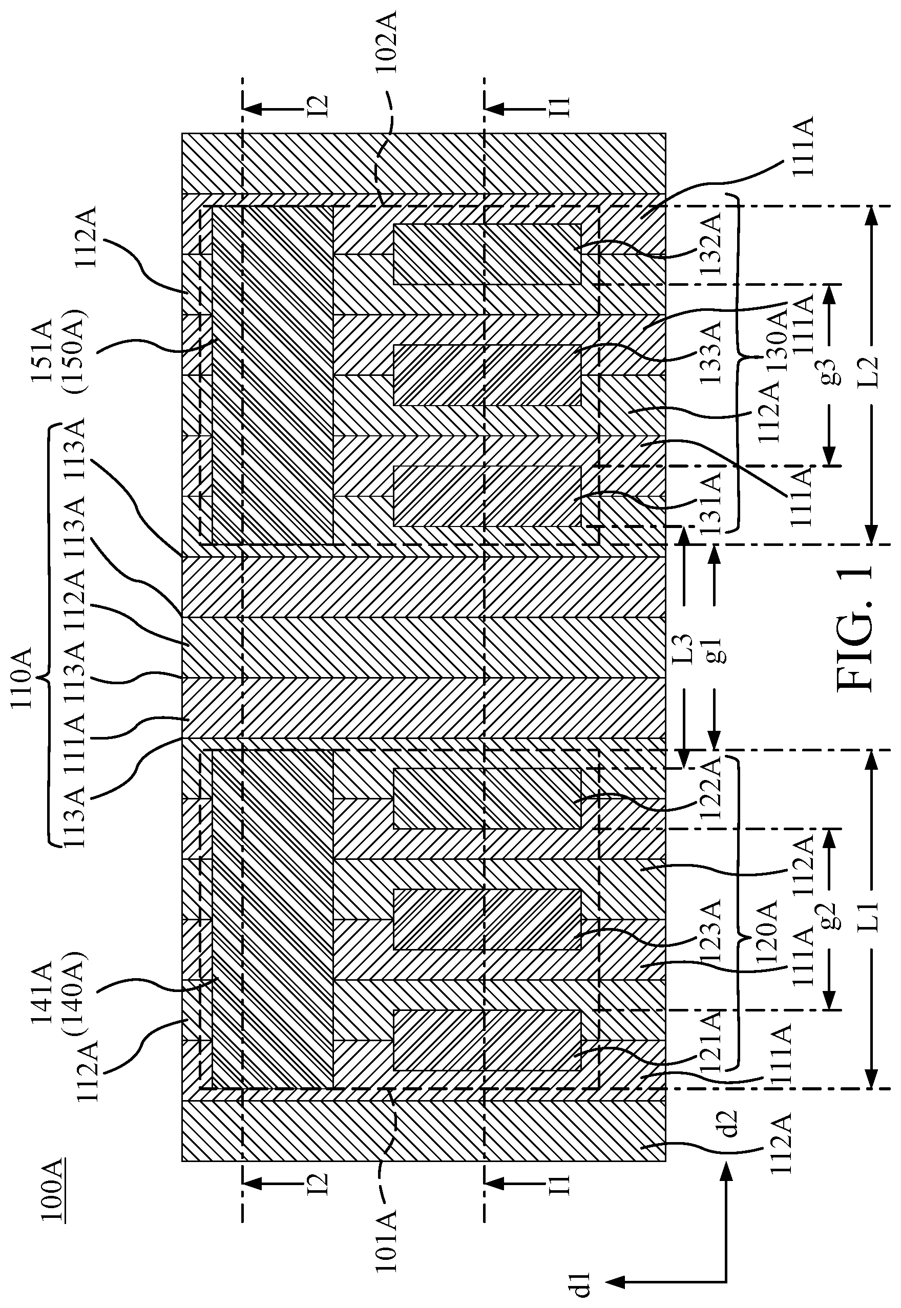
is a top view of a semiconductor device 100 A according to according to some embodiments of the present disclosure, and, in order to clarify the features, some layers or components of the semiconductor device 100 A are omitted in the figure. In this embodiment, the semiconductor device 100 A has a substrate 110 A, a GaN-based HEMT 120 A, a GaN-based HEMT 130 A, an interconnection 140 A, and an interconnection 150 A.
The substrate 110 A has a plurality of first-type doped semiconductor regions 111 A and a plurality of second-type doped semiconductor regions 112 A. The first-type doped semiconductor regions 111 A and the second-type doped semiconductor regions 112 A extend lengthwise along the first direction d 1 . The first-type doped semiconductor regions 111 A and the second-type doped semiconductor regions 112 A are alternately arranged along the second direction d 2 . The second direction d 2 is different from the first direction d 1 . For example, the first direction d 1 and the second direction d 2 in the embodiment are perpendicular to each others.
In the semiconductor device 100 A, the GaN-based HEMT 120 A and the GaN-based HEMT 130 A are disposed over the substrate 110 A. In one aspect, the GaN-based HEMT 120 A covers a region 101 A on the first-type doped semiconductor regions 111 A and the second-type doped semiconductor regions 112 A in the substrate 110 A. The GaN-based HEMT 130 A covers a region 102 A on the first-type doped semiconductor regions 111 A and the second-type doped semiconductor regions 112 A in the substrate 110 A. The region 101 A is different from the region 102 A. In the second direction d 2 , a gap g 1 is positioned between the region 101 A and the region 102 A.
In this embodiment, the first-type doped semiconductor regions 111 A and the second-type doped semiconductor regions 112 A form a plurality of junctions 113 A. The gap g 1 between the region 101 A and the region 102 A spans across at least two junctions 113 A. For example, the gap g 1 of this embodiment spans across four junctions 113 A.
is a side sectional view of the semiconductor device 100 A according to a cutting plan line I 1 in . The GaN-based HEMT 120 A of this embodiment has a heterojunction area 125 A being disposed between two nitride-based semiconductor layers 103 A, 104 A. The GaN-based HEMT 120 A has a 2DEG region 126 A adjacent to the heterojunction area 125 A. In other words, the heterojunction area 125 A is the heterojunction between the two nitride-based semiconductor layers 103 A, 104 A in the region 101 A.
The GaN-based HEMT 130 A has a heterojunction area 135 A being disposed between the two nitride-based semiconductor layers 103 A, 104 A. The GaN-based HEMT 130 A has a 2DEG region 136 A adjacent to the heterojunction area 135 A. The heterojunction area 135 A is the heterojunction between the two nitride-based semiconductor layers 103 A, 104 A in the region 102 A.
In an embodiment, the nitride-based semiconductor layer 104 A is disposed on the nitride-based semiconductor layer 103 A. The nitride-based semiconductor layer 104 A has a bandgap greater than a bandgap of the nitride semiconductor layer 103 A. Therefore, the 2DEG regions 126 A, 136 A are formed in the regions 101 A, 102 A, respectively.
In this embodiment, four junctions 113 A are located between the region 101 A and the region 102 A. Consequently, a voltage of the substrate 110 A in the region 101 A will not be affected by voltage changes in the region 102 A.
Moreover, a pair of S/D electrodes 121 A, 122 A are disposed on the nitride-based semiconductor layer 104 A. A gate electrode 123 A is disposed on the nitride-based semiconductor layer 104 A. The gate electrode 123 A is disposed between the S/D electrodes 121 A, 122 A. A pair of S/D electrodes 131 A, 132 A are disposed on the nitride-based semiconductor layer 104 A. A gate electrode 133 A is disposed on the nitride-based semiconductor layer 104 A. The gate electrode 133 A is disposed between the S/D electrodes 131 A, 132 A. The S/D electrodes 121 A, 122 A and the gate electrode 123 A are located in the region 101 A. The S/D electrodes 131 A, 132 A and the gate electrode 133 A are located in the region 102 A. The voltage of the substrate 110 A in the region 101 A will not be affected while the voltage of the substrate 110 A in the region 102 A is changed by the S/D electrodes 131 A, 132 A and the gate electrode 133 A.
For example, each of the S/D electrodes 121 A, 122 A, 131 A, 132 A includes one or more conformal conductive layers. In some embodiments, the S/D electrodes 121 A, 122 A, 131 A, 132 A can includes, for example but are not limited to, metals, alloys, doped semiconductor materials (such as doped crystalline silicon), other conductor materials, or combinations thereof. The exemplary materials of the S/D electrodes 121 A, 122 A, 131 A, 132 A can include, for example but are not limited to, Ti, AlSi, TiN, or combinations thereof. In some embodiments, each of the S/D electrodes 121 A, 122 A, 131 A, and 132 A forms ohmic contact with the nitride-based semiconductor layer 104 . The ohmic contact can be achieved by applying Ti, Al, or other suitable materials for the S/D electrodes 121 A, 122 A, 131 A, and 132 A. In some embodiments, a dielectric layer (not illustrated), such as SiN, can be disposed between the nitride-based semiconductor layer 104 and the S/D electrodes 121 A, 122 A, 131 A, and 132 A.
Referring to , the interconnection 140 A is disposed over the substrate 110 A. The interconnection 150 A is disposed over the substrate 110 A. In one aspect, in the second direction d 2 , lengths of the interconnection 140 A and the region 101 A may be the same. Lengths of the interconnection 150 A and the region 102 A may also be the same in the second direction d 2 . Optionally, the lengths may be different depending upon the device application.
is a side sectional view of the semiconductor device according to a cutting plan line I 2 in . The interconnection 140 A is disposed over the substrate 110 A. Some of the first-type doped semiconductor regions 111 A and the second-type doped semiconductor regions 112 A are located under the interconnection 140 A. The interconnection 140 A passes through the two nitride-based semiconductor layers 103 A, 104 A. The interconnection 140 A is electrically connected to the substrate 110 A. A portion of the region 101 A forms an interface 141 A with the interconnection 140 A. In other words, the interconnection 140 A connects the substrate 110 A through the interface 141 A.
The interconnection 150 A is disposed over the substrate 110 A. Some of the first-type doped semiconductor regions 111 A and the second-type doped semiconductor regions 112 A are located under the interconnection 150 A. The interconnection 150 A passes through the two nitride-based semiconductor layers 103 A, 104 A as well. The interconnection 150 A is electrically connected to the substrate 110 A. A portion of the region 102 A forms an interface 151 A with the interconnection 150 A. In other words, the interconnection 150 A connects the substrate 110 A through the interface 151 A.
Therefore, the voltage of the substrate 110 A in the regions 101 A, 102 A can be independently controlled by the interconnections 140 A, 150 A, respectively. The voltage of the substrate 110 A in the region 101 A can remain in a selected range by applying electrical signals to interconnection 140 A. The voltage of the substrate 120 A in the region 102 A can remain in a selected range by applying electrical signals to interconnection 150 A. The voltage may be the same or different.
In contrast, when two GaN-based HEMTs are disposed on the same substrate without first-type and second-type doped semiconductor regions described above, it is difficult to operate each of the GaN-based HEMTs independently. Without the doped semiconductor regions, a substrate effect would occur such that the two GaN-based HEMTs might affect each other. As used herein, the substrate effect means the two GaN-based HEMTs share the same substrate voltage. As such, it is difficult to operate the two GaN-based HEMTs independently.
As seen in , the interface 141 A is separated from the interface 151 A by at least two junctions 113 A. A vertical projection of a portion of the nitride-based semiconductor layer 103 A on the substrate 110 A is between the interfaces 141 A, 151 A. The portion of the nitride-based semiconductor layer 103 A at least spans across two entire doped semiconductor regions 111 A, 112 A. For example, the interface 141 A is separate from the interface 151 A by four junctions 113 A. The portion of the nitride-based semiconductor layer 103 A between the interfaces 141 A, 151 A spans across two entire first-type doped semiconductor regions 111 A and one entire second-type doped semiconductor region 112 A. The voltage of the substrate 110 A in region 101 A will not be affected by the voltage in the region 102 A.
In one aspect, the first-type doped semiconductor regions 111 A may include p-type dopants. The second-type doped semiconductor regions 112 A may include n-type dopants. The junctions 113 A include at least two p-n junctions. The junctions 113 A also include a p-n-p structures. In other words, the p-n-p structures between the region 101 A and the region 102 A form the two p-n junctions. For example, the semiconductor device 100 A of this embodiment has four p-n junctions located between the region 101 A and the region 102 A. In other words, the gap g 1 spans across four p-n junctions 113 A. The vertical projection of the portion of the nitride-based semiconductor layer 103 A on the substrate 110 B spans across a p-n-p structure.
For example, the p-type dopants can include, for example but are not limited to, Be, Mg, Zn, Cd. The n-type dopants can include, for example but are not limited to, Si.
Referring to , the pair of S/D electrodes 121 A, 122 A are arranged along the second direction d 2 with a source-drain spacing g 2 . The interface 141 A has a length L 1 along the second direction d 2 greater than the source-drain spacing g 2 . The part of S/D electrodes 131 A, 132 A are arranged along the second direction d 2 with a source-drain spacing g 3 . The interface 151 A has a length L 2 along the second direction d 2 that may optionally be greater than the source-drain spacing g 3 . Other configurations may include the same spacing depending on the device application.
As a result of this configuration, the interconnection 140 A can control the voltage under the S/D electrodes 121 A, 122 A. The interconnection 150 A can control the voltage under the S/D electrodes 131 A, 132 A.
Moreover, the shortest distance, which is gap g 1 , from the interconnection 140 A to the interconnection 150 A may be less than the shortest distance L 3 from the S/D electrodes 121 A, 122 A to the S/D electrodes 131 A, 132 A.
Referring to , the substrate 110 A of the embodiment includes base layer 115 A, and insulating layer 114 A. The material of the base layer 115 A may include silicon. Alternatively, the base layer may be germanium, silicon carbide, sapphire, or other known substrate materials. The insulating layer 114 A is disposed on the base layer 115 A and may be silicon dioxide, silicon nitride, mixtures thereof, or other known nitrides, oxides, or other insulator materials. The first-type doped semiconductor regions 111 A and the second-type doped semiconductor regions 112 A are disposed on the insulating layer 114 . The insulating layer 114 can block current between the base layer 115 A and the first and second-type doped semiconductor regions 111 A and 112 A. For example, the insulating layer 114 can be formed by a single layer or more layers of dielectric materials. The exemplary dielectric materials can include, for example but are not limited to, one or more oxide layers, a SiO x layer, a SiN x layer, a high-k dielectric material (e.g., HfO 2 , Al 2 O 3 , TiO 2 , HfZrO, Ta 2 O 3 , HfSiO 4 , ZrO 2 , ZrSiO 2 , etc), or combinations thereof.
In some embodiments, a nucleation layer can be disposed on the insulating layer 114 A. The first and second-type doped semiconductor regions 111 A and 112 A can be formed on the nucleation layer. In some embodiments, a buffer layer can be disposed on the first and second-type doped semiconductor regions 111 A and 112 A. The nitride-based semiconductor layer 103 A can be formed on the buffer layer.
The material of the first-type doped semiconductor regions 111 A and the second-type doped semiconductor regions 112 A may include GaN. In some embodiments, the first-type doped semiconductor regions 111 A and the second-type doped semiconductor regions 112 A may include, for example but not limited to, nitrides or group III-V compounds, such as GaN, GaAs, InN, AlN, InGaN, AlGaN, InAlGaN, or combinations thereof.
The material of the nitride-based semiconductor layer 103 A may include GaN. The material of the nitride-based semiconductor layer 104 A may include AlGaN. The bandgap of the nitride-based semiconductor layer 104 A is greater than the bandgap of the nitride-based semiconductor layer 103 A. Therefore, 2DEG regions 126 A, 136 A are formed. In some embodiments, the nitride-based semiconductor layers 103 A, 104 A may include, for example but are not limited to, nitrides or group III-V compounds, such as GaN, AlN, InN, In x Al y Ga (1-x-y) N where x+y≤1, Al y Ga (1-y) N where y≤1, while the bandgap of the nitride-based semiconductor layer 104 A is greater than the bandgap of the nitride-based semiconductor layer 103 A, and a 2DEG is formed. Alternatively, other binary, ternary or quaternary III-V semiconductors may also be used as long as a difference in bandgaps creates a heterojunction and forms 2DEG regions in the respective devices.
The semiconductor device 100 A further includes a passivation layer 180 A and connecting pads 161 A, 162 A, 163 A, 171 A, 172 A, and 173 A. The connecting pads 161 A, 162 A penetrate the passivation layer 180 in the region 101 A and electrically connect the S/D electrodes 121 A, 122 A respectively. The connecting pad 163 A penetrates the passivation layer 180 in the region 101 A and electrically connects the gate electrode 123 A. The connecting pads 171 A, 172 A penetrate the passivation layer 180 in the region 102 A and electrically connect the S/D electrodes 131 A, 132 A respectively. The connecting pad 173 A penetrates the passivation layer 180 in the region 102 A and electrically connects the gate electrode 133 A.
The passivation layer 180 A covers the S/D electrodes 121 A, 122 A, 131 A, 132 A and the gate electrodes 123 A, 133 A for a protection purpose. The exemplary materials of the passivation layer 180 A can include, for example but are not limited to, SiN x , SiO x , SiON, SiC, SiBN, SiCBN, oxides, nitrides, or combinations thereof. In some embodiments, the passivation layer 180 A is a multi-layered structure, such as a composite dielectric layer of Al 2 O 3 /SiN, Al 2 O 3 /SiO 2 , AlN/SiN, AlN/SiO 2 , or combinations thereof.
The semiconductor device 100 A includes a first-type doped gate layers 124 A and 134 A. The first-type doped gate layer 124 A is disposed between the gate electrode 123 A and the nitride-based semiconductor layer 104 A. The first-type doped gate layer 134 A is disposed between the gate electrode 133 A and the nitride-based semiconductor layer 104 A. For example, the first-type doped gate layers 124 A, 134 A are doped with p-type dopants. Therefore, the GaN-based HEMT 120 A and the GaN-based HEMT 130 A can provide a normally-off operation, typically referred to as enhancement mode. The p-type dopants can include, for example but are not limited to, Be, Mg, Zn, Cd.
In some embodiments, the first-type doped gate layers 124 A, 134 A can be omitted. Therefore, the semiconductor devices in these embodiments can provide a normally-on operation, typically referred to as depletion mode. Alternatively, one device may operate as an enhancement mode device (with a doped layer) and one device may operate as a depletion mode device.
Referring to , the semiconductor device 100 A includes connecting pads 191 A, 192 A. The connecting pad 191 A penetrates the passivation layer 180 A and electrically connects to the interconnection 140 A. The connecting pad 192 A penetrates the passivation layer 180 A and electrically connects to the interconnection 150 A. In some embodiments, each of the connecting pads 191 A, 192 A may include a via and a metal line. The via can penetrate the passivation layer 180 A and electrically connect to the interconnection 140 A. The metal line is disposed on the passivation layer 180 A and in contact with the via. The via and the metal line may include metals or metal compounds. The exemplary materials of the metals or metal compounds can include, for example but are not limited to, W, Au, Pd, Ti, Ta, Co, Ni, Pt, Mo, TiN, TaN, metal alloys thereof, or other metallic compounds.
The interconnection 140 A penetrates the nitride-based semiconductor layers 103 A, 104 A with extending along sidewalls of the nitride-based semiconductor layers 103 A, 104 A. A bottom most portion 142 A of the interconnection 140 A forms the interface 141 A. A bottom most portion 152 A of the interconnection 150 A forms the interface 151 A. The interconnections 140 A and 150 A can be electrically coupled to external pads through the connecting pads 191 A, 192 A, respectively. For example, the connecting pads 191 A, 192 A can be electrically coupled to different voltage sources.
is a side section view of a semiconductor device according to some embodiments of the present disclosure. In some embodiments, the interconnections 140 A, 150 A may penetrate the passivation layer 180 A, the nitride-based semiconductor layer 104 A, and the nitride-based semiconductor layer 103 A. In some embodiments, the interconnections 140 A, 150 A may have portions over the passivation layer 180 A.
to 11 are side sectional views of manufacturing method of semiconductor device 100 B according to some embodiments of the present disclosure. Referring to , the manufacturing method of this embodiment includes providing a undoped substrate 1101 B. The undoped substrate 1101 B has a base layer 115 B, an insulating layer 114 B, and a undoped layer 116 B. The insulating layer 114 B is disposed on the base layer 115 B. The undoped layer 116 B is disposed on the insulating layer 114 B. In some embodiments of the present disclosure, a nucleation layer is disposed on the insulating layer. The undoped layer 116 B is disposed on the nucleation layer. In some embodiments, the undoped layer 116 B includes nitrides or group III-V compounds. In some embodiments, the undoped layer 116 B may include, for example but are not limited to, GaN, AlN, InN, In x Al y Ga (1-x-y) N where x+y≤1, Al y Ga (1-y) N where y≤1. For example, the undoped layer 116 B is an undoped GaN layer. In some embodiments, the formation of the undoped layer 116 B may include forming a buffer layer for reducing a difference in thermal coefficient or lattice number.
Referring to , the manufacturing method of the embodiment includes forming a plurality of first-type doped semiconductor regions 111 B and second-type doped semiconductor regions 112 B with a plurality of junctions 113 B in a substrate 110 B. In some embodiments, the formation of the first-type doped semiconductor regions 111 B and second-type doped semiconductor regions 112 B is achieved by at least one doping process. In one aspect, the initially undoped layer 116 B can be doped with the second dopant after the first-type doped semiconductor regions 111 B are doped with the first dopant, and vice versa. The first-type doped semiconductor regions 111 B and second-type doped semiconductor regions 112 B are alternately arranged along the second direction d 2 . The junctions 1113 B are formed among the first-type doped semiconductor regions 111 B and second-type doped semiconductor regions 112 B. For example, the first-type doped semiconductor regions 111 B are formed by doping p-type dopants. The second-type doped semiconductor regions 112 B are formed by doping n-type dopants.
Referring to , the manufacturing method of the embodiment includes forming a nitride-based semiconductor layer 103 B above the substrate 110 B; forming a nitride-based semiconductor layer 104 B on the nitride-based semiconductor layer 103 B. the nitride-based semiconductor layer 104 B has a bandgap greater than a bandgap of the nitride-based semiconductor layer 103 B.
For example, a material of the nitride-based semiconductor layer 103 B may include GaN. A material of the nitride-based semiconductor layer 104 B may include AlGaN. A heterojunction is formed between the nitride-based semiconductor layer 103 B and the nitride-based semiconductor layer 104 B, and a 2DEG is formed. In some embodiments, prior to the formation of the nitride-based semiconductor layer 103 B, the manufacturing method of the embodiment may further include forming a nucleation layer or a buffer layer for reducing a difference in thermal coefficient or lattice number. The material of the nucleation layer or the buffer layer can be selected according to the properties of the substrate 110 B and the nitride-based semiconductor layer 103 B.
The manufacturing method of the embodiment further includes forming a pair of S/D electrodes 121 B, 122 B and a pair of S/D electrodes 131 B, 132 B on the nitride-based semiconductor layer 104 B; forming a gate electrode 123 B and a gate electrode 133 B on the nitride-based semiconductor layer 104 B. The gate electrode 123 B is present between the S/D electrodes 121 B, 122 B. The gate electrode 133 B is present between the S/D electrodes 131 B, 132 B.
The S/D electrodes 121 B, 122 B and the gate electrode 123 B are disposed on the region 101 B on the substrate 110 B. The heterojunction in the region 101 B is the heterojunction area 125 B. The 2DEG in the region 101 B is the 2DEG region 126 B. The 2DEG region 126 B is adjacent to the heterojunction area 125 B.
The S/D electrodes 131 B, 132 B and the gate electrode 13 B are disposed on the region 102 B on the substrate 110 B. The heterojunction in the region 102 B is the heterojunction area 135 B. The 2DEG in the region 102 B is the 2DEG region 136 B. The 2DEG region 136 B is adjacent to the heterojunction area 135 B.
Referring to , the manufacturing method of the embodiment includes disposing a passivation layer 180 B with a plurality of connecting pads 161 B, 162 B, 163 B, 171 B, 172 B, and 173 B. The connecting pads 161 B, 162 B, 163 B, 171 B, 172 B, and 173 B are electrically connected to the S/D electrodes 121 B, 122 B, the gate electrode 123 B, the S/D electrodes 131 B, 132 B, and the gate electrode 133 B. Therefore, a HEMT part of the semiconductor device 100 B is formed.
The semiconductor device 100 B includes a first-type doped gate layers 124 B and 134 B. The first-type doped gate layer 124 B is disposed between the gate electrode 123 B and the nitride-based semiconductor layer 104 B. The first-type doped gate layer 134 B is disposed between the gate electrode 133 B and the nitride-based semiconductor layer 104 B.
Referring to , on the other part of the substrate 110 B, the manufacturing method of the embodiment includes removing portions of the nitride-based semiconductor layer 103 B and the nitride-based semiconductor layer 104 B to form a trench 105 B and a trench 106 B separated from each other, so as to expose a top portion of the substrate 110 B. I In the second direction d 2 , the trench 105 B and the trench 106 are separated by two junctions 103 B of the substrate 110 B.
Referring to , the manufacturing method of the embodiment includes forming interconnections 140 B, 150 B in the trenches 105 B, 106 B, respectively, and in contact with the top portion of the substrate 110 B so as to form an interface 141 B and an interface 151 B, wherein vertical projections of the interfaces 141 B, 151 B on the substrate 110 B are at least separated from each other by at least two of the junctions 113 B.
Referring to , forming the interconnections 140 B, 150 B includes forming a blanket conductive layer 107 B above the nitride-based semiconductor layer 104 B. Some portions of the blanket conductive layer 107 B are present in the trenches 105 B, 106 B.
Referring to , forming the interconnections 140 B, 150 B includes patterning the blanket conductive layer 107 B to form the interconnections 140 B, 150 B separated from each other. Also, a passivation layer 180 B with connecting pads 191 B, 192 B is disposed on the interconnections 140 B, 150 B. Therefore, an interconnection part of the semiconductor device 100 B is formed.
For example, referring to , in the embodiment, the junctions 113 B of the substrate 110 B are p-n junctions. The vertical projection of the portion of the nitride-based semiconductor layer 103 B on the substrate 110 B spans across two p-n junctions 113 B. is a top view of the semiconductor device 100 B according to the embodiment of the present disclosure. Two p-n junctions 113 B separate the region 101 B and the region 102 B. The GaN-based HEMT 120 B and the interconnection 140 B are disposed in the region 101 B. The GaN-based HEMT 130 B and the interconnection 150 B are disposed in the region 102 B.
is a top view of a semiconductor device 100 C according to some embodiments of the present disclosure. In another embodiment, GaN-based HEMTs 120 C, 130 C are similar to the GaN-based HEMTs 120 A, 130 A. On the substrate 110 C, the interconnection 140 C, the S/D electrodes 121 C, 122 C, and the gate electrode 123 C are disposed in the region 101 C, and the interconnection 150 C, the S/D electrodes 131 C, 132 C, and the gate electrode 133 C are disposed in the region 102 C.
In this embodiment, the first-type doped semiconductor regions 111 C are doped with n-type dopants. The second-type doped semiconductor regions 112 C are doped with p-type dopants. A plurality of junctions 113 C are formed among the first-type doped semiconductor regions 111 C and the second-type doped semiconductor regions 112 C.
is a top view of a semiconductor device 100 D according to some embodiments of the present disclosure. In the embodiment, the GaN-based HEMT 120 D includes a pair of S/D electrodes 121 D, 122 D arranged along the first direction d 1 . The interface 141 D of the interconnection 140 D and vertical projections of the S/D electrodes 121 D, 122 D on the substrate 110 D are arranged along the first direction d 1 . The first-type doped semiconductor regions 111 D, the second-type doped semiconductor regions 112 D, and the junctions 113 D extend along the first direction d 1 .
The GaN-based HEMT 130 D includes a pair of S/D electrodes 131 D, 132 D arranged along the first direction d 1 . The interface 151 D of the interconnection 150 D and vertical projections of the S/D electrodes 131 D, 132 D on the substrate 110 D are arranged along the first direction d 1 .
is a top view of a semiconductor device 100 E according to some embodiments of the present disclosure. In the embodiment, the GaN-based HEMT 120 E includes a pair of S/D electrodes 121 E, 122 E and gate electrode 123 E arranged along the first direction d 1 . The interface 141 E of the interconnection 140 E and vertical projections of the S/D electrodes 121 E, 122 E on the substrate 110 E are within one of the plurality of first-type doped semiconductor regions 111 E and second-type doped semiconductor regions 112 E. In other words, the interface 141 E and the vertical projections of the S/D electrodes 121 E, 122 E on the substrate 110 E are located between two junctions 113 E.
The GaN-based HEMT 130 E includes a pair of S/D electrodes 131 E, 132 E and gate electrode 133 E arranged along the first direction d 1 . The interface 151 E of the interconnection 150 E and vertical projections of the S/D electrodes 131 E, 132 E on the substrate 110 E are within one of the firs-type dopes region 111 E and second-type doped semiconductor regions 112 E. In other words, the interface 151 E and the vertical projections of the S/D electrodes 131 E, 132 E on the substrate 110 E are located between two junctions 113 E.
is a top view of a semiconductor device 100 F according to some embodiments of the present disclosure. In the embodiment, the GaN-based HEMT 120 F includes a pair of S/D electrodes 121 F, 122 F and gate electrode 123 F arranged along the first direction d 1 . The S/D electrodes 121 F, 122 F and the gate electrode 123 F are similar to the S/D electrodes 121 E, 122 E and gate electrode 123 E. The interface 141 F of the interconnection 140 F spans across two junctions 113 F. The S/D electrodes 121 F, 122 F and the gate electrode 123 F are disposed on one of the first-type doped semiconductor region 111 F or second-type doped semiconductor region 112 F between the two junctions 113 F in the first direction d 1 .
The GaN-based HEMT 130 F includes a pair of S/D electrodes 131 F, 132 F and gate electrode 133 F arranged along the first direction d 1 . The S/D electrodes 131 F, 132 F and the gate electrode 133 F are similar to the S/D electrodes 131 E, 132 E and gate electrode 133 E. The interface 151 F of the interconnection 150 F spans across two junctions 113 F. The S/D electrodes 131 F, 132 F and the gate electrode 133 F are disposed on one of the first-type doped semiconductor region 111 F or second-type doped semiconductor region 112 F between the two junctions 113 F.
is a top view of a semiconductor device 100 G according to some embodiments of the present disclosure. In the embodiment, the GaN-based HEMT 120 G includes a pair of S/D electrodes 121 G, 122 G and gate electrode 123 G arranged along the first direction d 1 . The S/D electrodes 121 G, 122 G and gate electrode 123 G are disposed on one of the junctions 113 G formed among the first-type doped semiconductor regions 111 G and the second-type doped semiconductor regions 112 G of the substrate 110 G.
The GaN-based HEMT 130 G includes a pair of S/D electrodes 131 G, 132 G and gate electrode 133 G arranged along the first direction d 1 . The S/D electrodes 131 G, 132 G and gate electrode 133 G are disposed on one of the junctions 113 G form among the first-type doped semiconductor regions 111 G and the second-type doped semiconductor regions 112 G of the substrate 110 G.
is a top view of a semiconductor device 100 H according to some embodiments of the present disclosure. In the embodiment, the GaN-based HEMT 120 H includes a pair of S/D electrodes 121 H, 122 H and gate electrode 123 H arranged along the second direction d 2 . In the first direction d 1 , the GaN-based HEMT 120 H is disposed between the interconnections 140 H and 141 H. The interconnections 140 H and 141 H are arranged along the first direction d 1 .
The GaN-based HEMT 130 H includes a pair of S/D electrodes 131 H, 132 H and gate electrode 133 H arranged along the second direction d 2 . In the first direction d 1 , the GaN-based HEMT 130 H is disposed between the interconnections 150 H and 151 H. The interconnections 150 H and 151 H are arranged along the first direction d 1 .
In this embodiment, a vertical projection of each of the S/D electrodes 121 H, 122 H on the interconnection 141 H is directly above the interface. The interface is form between the interconnection 141 H and the substrate 110 H.
is a top view of a semiconductor device 100 I according to some embodiments of the present disclosure. In the embodiment, the substrate 110 I has an area A and an area B. The first-type doped semiconductor regions 111 I and the second-type doped semiconductor regions 112 I in the area A are extending along a third direction d 3 . The first-type doped semiconductor regions 111 I and the second-type doped semiconductor regions 112 I in the area B are extending along a first direction d 1 . The first direction d 1 is different from the third direction d 3 . The GaN-based HEMT 120 I includes a pair of S/D electrodes 121 I, 122 I and gate electrode 123 I arranged along the second direction d 2 . The GaN-based HEMT 130 I includes a pair of S/D electrodes 131 I, 1321 and gate electrode 133 I arranged along the second direction d 2 .
The GaN-based HEMT 120 I is disposed in the area A. The GaN-based HEMT 130 I is disposed in the area B. The interconnection 140 I and the interconnection 150 I are disposed in the area A. The GaN-based HEMT 120 I and the interconnection 140 I span across the same junctions 113 I. The GaN-based HEMT 120 I and the interconnection 140 I span across the same junctions 113 I.
is a top view of a semiconductor device 100 J according to some embodiments of the present disclosure. In the embodiment, a vertical projection of the interconnection 140 J on the substrate 110 J at least has a L-shaped profile. A vertical projection of the interconnection 150 J on the substrate 110 J at least has a L-shaped profile. The interconnection 140 J is adjacent to the S/D electrodes 121 J, 122 J and the gate electrode 123 J of the GaN-based HEMT 120 J. The interconnection 150 J is adjacent to the S/D electrodes 131 J, 132 J and the gate electrode 133 J of the GaN-based HEMT 130 J.
is a top view of a semiconductor device 100 K according to some embodiments of the present disclosure. In the embodiment, a vertical projection of the interconnection 140 K on the substrate 110 K comprises a ring shape, and a vertical projection of the GaN-based HEMT 120 K on the substrate 110 K is within the ring-shaped vertical projection of the interconnection 140 K. A vertical projection of the interconnection 150 K on the substrate 110 K comprises a ring shape, and a vertical projection of the GaN-based HEMT 130 K on the substrate 110 K is within the ring-shaped vertical projection of the interconnection 140 K. The GaN-based HEMT 120 K includes a pair of S/D electrodes 121 K, 122 K and gate electrode 123 K arranged along the second direction d 2 . The GaN-based HEMT 130 K includes a pair of S/D electrodes 131 K, 132 K and gate electrode 133 K arranged along the second direction d 2 .
is a top view of a semiconductor device 100 J according some embodiments of the present disclosure. In the embodiment, a vertical projection of the interconnection 140 J on the substrate 110 J is directly above the GaN-based HEMT 120 J in the first direction d 1 . A vertical projection of the interconnection 150 J on the substrate 110 J is directly below the GaN-based HEMT 130 J in the first direction d 1 . The GaN-based HEMT 120 J includes a pair of S/D electrodes 121 J, 122 J and gate electrode 123 J arranged along the second direction d 2 . The GaN-based HEMT 130 J includes a pair of S/D electrodes 131 J, 132 J and gate electrode 133 J arranged along the second direction d 2 .
is a top view of a semiconductor device 100 K according some embodiments of the present disclosure. In the embodiment, a GaN-based HEMT 200 K is disposed on the substrate 110 K to cover the region 101 K of the plurality of first-type doped semiconductor regions 111 K and second-type doped semiconductor regions 112 K in the substrate 110 K. The GaN-based HEMT 200 K including a heterojunction area being disposed between the two nitride-based semiconductor layers with another 2DEG region formed in the region of the heterojunction area.
The GaN-based HEMT 200 K has S/D electrodes 201 K, 203 K, and a gate electrode 202 K arranging along the second direction d 2 . The GaN-based HEMT 120 K has S/D electrodes 121 K, 122 K, and a gate electrode 123 K arranging along the second direction d 2 . The GaN-based HEMT 130 K has S/D electrodes 121 K, 122 K, and a gate electrode 123 K arranging along the second direction d 2 . The GaN-based HEMT 120 K and the GaN-based HEMT 200 K cover the region 101 K. Some of the junctions 113 K among the first and second-type doped semiconductor regions 111 K, 112 K separate the GaN-based HEMT 200 K and the GaN-based HEMT 130 K.
Although not shown in the drawings, it is understood that additional GaN-based HEMTs may be integrated on a single substrate in the manner described for the devices above such that an arbitrary number of HEMT devices may be integrated in this manner. Furthermore, the above embodiments provide different configurations of the semiconductor devices, which will be advantageous to improve the flexibility. For example, the different configurations of the semiconductor devices can be selected according to process conditions, device sizes, device functions (e.g. low voltage, high voltage, or radio frequency application), or likes. Although not shown in the drawings, it is understood that above different configurations of the semiconductor devices can be integrated into a single chip or a circuit.
The foregoing description of the present invention has been provided for the purposes of illustration and description. It is not intended to be exhaustive or to limit the invention to the precise forms disclosed. Many modifications and variations will be apparent to the practitioner skilled in the art.
The embodiments were chosen and described in order to best explain the principles of the invention and its practical application, thereby enabling others skilled in the art to understand the invention for various embodiments and with various modifications that are suited to the particular use contemplated.
As used herein and not otherwise defined, the terms “substantially,” “substantial,” “approximately” and “about” are used to describe and account for small variations. When used in conjunction with an event or circumstance, the terms can encompass instances in which the event or circumstance occurs precisely as well as instances in which the event or circumstance occurs to a close approximation. For example, when used in conjunction with a numerical value, the terms can encompass a range of variation of less than or equal to ±10% of that numerical value, such as less than or equal to ±5%, less than or equal to ±4%, less than or equal to ±3%, less than or equal to ±2%, less than or equal to ±1%, less than or equal to ±0.5%, less than or equal to ±0.1%, or less than or equal to ±0.05%. The term “substantially coplanar” can refer to two surfaces within micrometers of lying along a same plane, such as within 40 within 30 within 20 within 10 or within 1 μm of lying along the same plane.
As used herein, the singular terms “a,” “an,” and “the” may include plural referents unless the context clearly dictates otherwise. In the description of some embodiments, a component provided “on” or “over” another component can encompass cases where the former component is directly on (e.g., in physical contact with) the latter component, as well as cases where one or more intervening components are located between the former component and the latter component.
While the present disclosure has been described and illustrated with reference to specific embodiments thereof, these descriptions and illustrations are not limiting. It should be understood by those skilled in the art that various changes may be made and equivalents may be substituted without departing from the true spirit and scope of the present disclosure as defined by the appended claims. The illustrations may not necessarily be drawn to scale. There may be distinctions between the artistic renditions in the present disclosure and the actual apparatus due to manufacturing processes and tolerances. Further, it is understood that actual devices and layers may deviate from the rectangular layer depictions of the FIGS. and may include angles surfaces or edges, rounded corners, etc. due to manufacturing processes such as conformal deposition, etching, etc. There may be other embodiments of the present disclosure which are not specifically illustrated. The specification and the drawings are to be regarded as illustrative rather than restrictive. Modifications may be made to adapt a particular situation, material, composition of matter, method, or process to the objective, spirit and scope of the present disclosure. All such modifications are intended to be within the scope of the claims appended hereto. While the methods disclosed herein have been described with reference to particular operations performed in a particular order, it will be understood that these operations may be combined, sub-divided, or re-ordered to form an equivalent method without departing from the teachings of the present disclosure. Accordingly, unless specifically indicated herein, the order and grouping of the operations are not limitations.
Figures (20)
Citations
This patent cites (16)
- US8866192
- US10163707
- US20110210377
- US20140048850
- US20160262228
- US20180076287
- US20190140088
- US20190288101
- US20200144382
- US101013724
- US103531615
- US103745989
- US105336771
- US106024878
- US106941117
- US411769