Abstract
A semiconductor device includes a semiconductor layer, first and second electrodes, one or more gate electrodes, and an array of structures. The semiconductor layer has first and second sides opposite to each other in a first direction. The semiconductor layer is single crystal silicon. The array of structures is in the semiconductor layer and arranged in a second direction perpendicular to the first direction and along a [100] direction of the single crystal silicon and in a third direction that is perpendicular to the first direction and not perpendicular to the second direction. A first distance between first and second ones of the structures adjacent to each other in the third direction is less than a second distance between the first one and a third one of the structures adjacent to the first one in the second direction.
Claims (12)
1. A semiconductor device, comprising: a semiconductor layer having first and second sides opposite to each other in a first direction, the semiconductor layer being single crystal silicon and including a first region of a first conductivity type, a second region of a second conductivity type, and a third region of the first conductivity type in this order in the first direction from the first side to the second side; a first electrode on the first side; a second electrode on the second side; an array of structures formed in the semiconductor layer and arranged in a second direction that is perpendicular to the first direction and along a [100] direction of the single crystal silicon and in a third direction that is perpendicular to the first direction and not perpendicular to the second direction; and a plurality of gate electrodes corresponding to the structures, respectively, wherein each of the structures includes a conductive portion electrically connected to the second electrode and an insulating portion surrounding the conductive portion, and a first distance between a first one of the structures and a second one of the structures adjacent to the first one in the third direction is less than a second distance between the first one and a third one of the structures adjacent to the first one in the second direction.
Show 11 dependent claims
2. The semiconductor device according to claim 1 , wherein the array of structures is regularly arranged in the second and third directions, and a first pitch of the array in the third direction is less than a second pitch of the array in the second direction.
3. The semiconductor device according to claim 1 , wherein the array of structures is regularly arranged in the second and third directions, and a first pitch of the array in the third direction is equal to a second pitch of the array in the second direction.
4. The semiconductor device according to claim 1 , wherein a ratio of the first distance divided by the second distance is in a range of 0.5 to 0.95.
5. The semiconductor device according to claim 1 , wherein the conductive portion of the first one of the structures has a first length in the third direction and a second length in the second direction, the first length being less than the second length.
6. The semiconductor device according to claim 1 , wherein the first one of the structures has a third length in the third direction and a fourth length in the second direction, the third length being greater than the fourth length.
7. The semiconductor device according to claim 1 , wherein the first region of the semiconductor layer includes a first part between the first one and the second one of the structures and a second part between the first one and the third one of the structures, and a concentration of a first-conductivity-type impurity in the first part is less than a concentration of the first-conductivity-type impurity in the second part.
8. The semiconductor device according to claim 1 , wherein each of the structures has a hexagonal shape in cross section.
9. The semiconductor device according to claim 1 , wherein the conductive portion in each of structures has a hexagonal shape in cross section.
10. The semiconductor device according to claim 1 , wherein the insulating portion in each of the structures has a hexagonal loop shape in cross section.
11. The semiconductor device according to claim 1 , wherein each of the gate electrodes is provided in the insulating portion of a corresponding one of the structures.
12. The semiconductor device according to claim 1 , wherein each of the gate electrodes has a hexagonal loop shape in cross section.
Full Description
Show full text →
CROSS-REFERENCE TO RELATED APPLICATION(S)
This application is based upon and claims the benefit of priority from Japanese Patent Application No. 2020-034118, filed on Feb. 28, 2020, the entire contents of which are incorporated herein by reference.
FIELD
Embodiments described herein relate generally to a semiconductor device.
BACKGROUND
Semiconductor devices such as a metal oxide semiconductor field effect transistor (MOSFET) are used for conversion of power, or the like. It is desirable that the on resistance of a semiconductor device be low.
BRIEF DESCRIPTION OF THE DRAWINGS
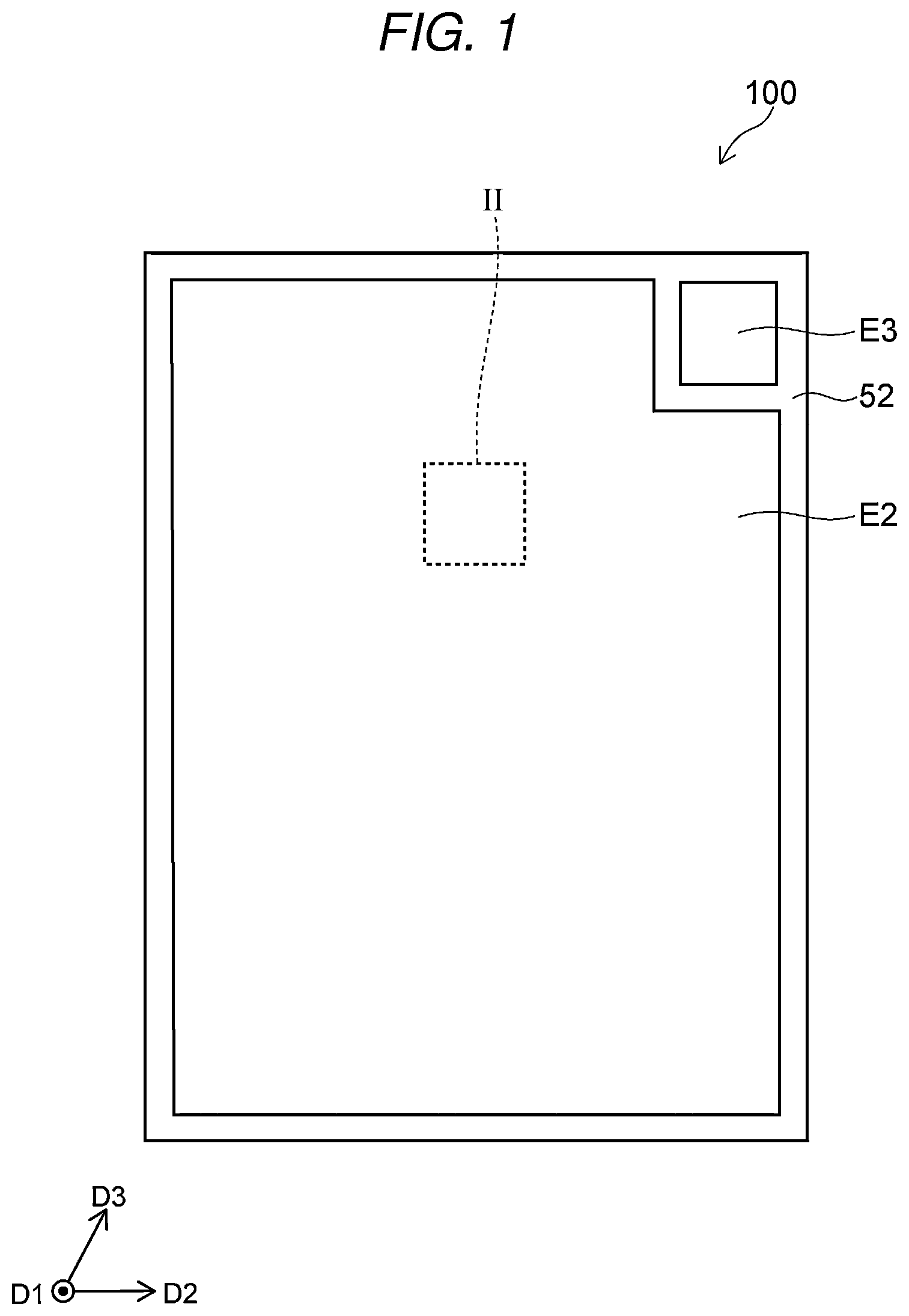
is a plan view of a semiconductor device according to a first embodiment.
is a plan view of part II of the semiconductor device illustrated in .
is a cross-sectional view of the semiconductor device taken along a line III-III in .
is a cross-sectional view of a semiconductor device taken along a line IV-IV in .
is a cross-sectional view of a part of a semiconductor device according to a first embodiment.
is another cross-sectional view of a part of a semiconductor device according to a first embodiment.
A and 7 B are cross-sectional views illustrating aspects of a process of manufacturing a semiconductor device according to the first embodiment.
A and 8 B are cross-sectional views illustrating aspects of a process of manufacturing a semiconductor device according to the first embodiment.
A and 9 B are cross-sectional views illustrating aspects of a process of manufacturing a semiconductor device according to the first embodiment.
A and 10 B are cross-sectional views illustrating aspects of a process of manufacturing a semiconductor device according to the first embodiment.
A and 11 B depict simulation results illustrating properties of a semiconductor device according to a reference example and a semiconductor device according to the first embodiment, respectively.
is a plan view of a part of a semiconductor device according to a first example of a first modification of the first embodiment.
is a plan view of a part of a semiconductor device according to a second example of a first modification of the first embodiment.
is a plan view of a part of a semiconductor device according to a second modification of the first embodiment.
is a plan view of a part of a semiconductor device according to a second embodiment.
is a cross-sectional view of a semiconductor device according to a second embodiment taken along a line XVI-XVI in .
is a cross-sectional view of a semiconductor device according to a second embodiment taken along a line XVII-XVII in .
DETAILED DESCRIPTION
In general, according to an embodiment, a semiconductor device includes a semiconductor layer, a first electrode, a second electrode, an array of structures, and one or more gate electrodes. The semiconductor layer has first and second sides opposite to each other in a first direction. The semiconductor layer of single crystal silicon and includes a first region of a first conductivity type, a second region of a second conductivity type, and a third region of the first conductivity type in this order in the first direction from the first side to the second side. The first electrode is on the first side. The second electrode is on the second side. The array of structures is formed in the semiconductor layer and arranged in a second direction that is perpendicular to the first direction and along a [100] direction of the single crystal silicon and in a third direction that is perpendicular to the first direction and not perpendicular to the second direction. Each of the structures includes a conductive portion electrically connected to the second electrode and an insulating portion surrounding the conductive portion. A first distance between a first one of the structures and a second one of the structures adjacent to the first one in the third direction is less than a second distance between the first one and a third one of the structures adjacent to the first one in the second direction.
Hereinafter, certain example embodiments will be described with reference to the drawings.
The drawings are schematic or conceptual, and relationships between the thickness and width of portions, ratios of sizes among portions, and the like are not necessarily the same as the actual values thereof. Even for identical portions depicted in different drawings, different dimensions and ratios may be shown in the drawings.
In the specification and the drawings of the present disclosure, components substantially identical to those already described are represented by identical reference numerals, and repeated description thereof may be omitted as appropriate.
In the following description and drawings, the labels n + , n − , p + , and p − represent a relatively high or low degree of concentration of each impurity type. That is, a symbol expressed with “ + ” shows that the impurity concentration is relatively higher than that of a symbol expressed without “ + ” or “ − ”, and a symbol expressed with “ − ” shows that the impurity concentration is relatively lower than that of the symbol expressed without “ + ” or “ − ”. When regions of these symbols each include both a p-type impurity and an n-type impurity, the symbols represent a relatively high or low degree of net impurity concentration that is obtained after the impurities offset each other.
Each embodiment in which p type and n type of each of semiconductor regions can be reversed with each other type in each of the following embodiments are possible.
First Embodiment
is a plan view of a semiconductor device according to a first embodiment.
is a plan view of a part II of the semiconductor device depicted in . In , a source electrode E 2 , an insulating layer 51 , an insulating layer 52 , and the like are omitted.
is a cross-sectional view of the semiconductor device taken along a line III-III in . is a cross-sectional view of the semiconductor device taken along a line IV-IV in .
A semiconductor device 100 according to the first embodiment is MOSFET. As illustrated in to 4 , the semiconductor device 100 according to the first embodiment includes a semiconductor layer SL, a drain electrode E 1 (first electrode), a source electrode E 2 (second electrode), and a gate pad E 3 (third electrode).
In description of each of the following embodiments, a first direction D 1 , a second direction D 2 , and a third direction D 3 are used for purposes of description. The first direction D 1 is a direction from the drain electrode E 1 to the semiconductor layer SL. The second direction D 2 is a direction perpendicular to the first direction D 1 . The third direction D 3 is a direction that is perpendicular to the first direction D 1 and is inclined to the second direction D 2 . The third direction D 3 is different from and not perpendicular to the second direction D 2 .
For purposes of the description, the direction from the drain electrode E 1 to the semiconductor layer SL is referred to as “upward”, and a direction opposite to the direction is referred to as “downward”. The directions are based on a relative positional relationship between the drain electrode E 1 and the semiconductor layer SL, and is not necessarily correlated with the direction of gravity.
As illustrated in , the source electrode E 2 and the gate pad E 3 are provided on an upper surface of the semiconductor device 100 . The source electrode E 2 is electrically separated from the gate pad E 3 . In an embodiment, a side of the semiconductor layer SL corresponding to the upper surface may be referred to as a first side.
As illustrated in , the drain electrode E 1 is provided on a lower surface of the semiconductor device 100 . In an embodiment, a side of the semiconductor layer SL corresponding to the lower surface may be referred to as a second side. The semiconductor layer SL is provided above the drain electrode E 1 . The semiconductor layer SL includes (or primarily consists of) single crystal silicon. The second direction D 2 corresponds to (or may be referred to as along) a [100] direction of a crystal plane of the single crystal silicon. The source electrode E 2 and the gate pad E 3 are provided on the semiconductor layer SL.
The semiconductor layer SL includes an n − -type (first conductive type) drift region 1 (a first semiconductor region), a p-type (second conductive type) base region 2 (a second semiconductor region), an n + -type source region 3 (a third semiconductor region), a p + -type contact region 4 , and an n + -type drain region 5 . The semiconductor device 100 also includes a plurality of gate electrodes 10 , and an array of structures 20 corresponding to the gate electrodes 10 , respectively.
The n + -type drain region 5 is provided on the drain electrode E 1 , and is electrically connected to the drain region E 1 . The n − -type drift region 1 is provided on the n + -type drain region 5 , and is electrically connected to the drain electrode E 1 through the n + -type drain region 5 . The p-type base region 2 is provided on the n − -type drift region 1 . The n + -type source region 3 and the p + -type contact region 4 are provided on the p-type base region 2 .
Each of the structures 20 includes an insulating portion 21 and a conductive portion 22 . The insulating portion 21 is adjacent to a part of the n − -type drift region 1 , the p-type base region 2 , and the n + -type source region 3 in the second direction D 2 and the third direction D 3 . The conductive portion 22 is provided in the insulating portion 21 . At least a part of the conductive portion 22 is adjacent to a part of the n − -type drift region 1 in the second direction D 2 and the third direction D 3 .
The gate electrode 10 is also provided in the insulating portion 21 of the semiconductor device 100 . The gate electrode 10 is provided around an upper part of the conductive portion 22 in the second direction D 2 and the third direction D 3 . Between the gate electrode 10 and the conductive portion 22 , a part of the insulating portion 21 is provided. Therefore, the gate electrode 10 is electrically separated from the conductive portion 22 .
The gate electrode 10 faces the p-type base region 2 through a gate insulating layer 11 in the second direction D 2 and the third direction D 3 . The gate electrode 10 may further face the n − -type drift region 1 and the n + -type source region 3 through the gate insulating layer 11 . In the semiconductor device 100 , a part of the insulating portion 21 functions as the gate insulating layer 11 .
As illustrated in , a plurality of gate electrodes 10 is arranged in the second direction D 2 and the third direction D 3 , and a plurality of structures 20 is arranged in the second direction D 2 and the third direction D 3 . The arrangement of the gate electrodes 10 and the arrangement of the structures 20 may be in a regular manner. For example, a continuous p-type base region 2 is provided around the plurality of gate electrodes 10 . The n + -type source region is one of a plurality of n + -type source regions 3 that are provided around the plurality of gate electrodes 10 .
As illustrated in , the insulating layer 51 is provided on the p-type base region 2 , the plurality of n + -type source regions 3 , the plurality of gate electrodes 10 , and the plurality of structures 20 . On the insulating layer 51 , a gate wiring 30 is provided. On the gate wiring 30 and the insulating layer 51 , the insulating layer 52 is provided. On the insulating layer 52 , the source electrode E 2 and the gate pad E 3 are provided.
The source electrode E 2 is provided on the p-type base region 2 , the plurality of n + -type source regions 3 , the plurality of gate electrodes 10 , and the plurality of structures 20 . The n + -type source regions 3 and the p + -type contact region 4 are electrically connected to the source electrode E 2 through a connection part 41 . The source electrode E 2 is electrically connected to the conductive portion 22 through a connection part 42 . The p-type base region 2 is electrically connected to the source electrode E 2 through the p + -type contact region 4 and the connection part 41 . In the semiconductor device 100 , a part of the connection part 41 is provided between the n + -type source regions 3 . The p + -type contact region 4 is disposed below the n + -type source regions 3 .
The gate electrodes 10 are electrically separated from the source electrode E 2 . The gate electrodes 10 are electrically connected to the gate wiring 30 through a connection part 43 . The gate wiring 30 is electrically connected to the gate pad E 3 . As illustrated in , the gate wiring 30 is one of a plurality of gate wirings 30 that are arranged in the third direction D 3 . Each of the gate wirings 30 is electrically connected to the plurality of gate electrodes 10 arranged in the second direction D 2 through a plurality of connection parts 43 .
are cross-sectional views illustrating a part of the semiconductor device according to the first embodiment. represent a part of cross-sectional views of taken along a line V-V.
As illustrated in , the semiconductor device have a first surface S 1 that is perpendicular to the second direction D 2 and a second surface S 2 that is inclined to the second direction D 2 . Specifically, the structures 20 each have a surface that is perpendicular to the [100] direction of a crystal plane of silicon and a surface that is inclined to the [100] direction.
A first distance Di 1 between the adjacent structures 20 in the third direction D 3 is shorter than a second distance Di 2 between the adjacent structures 20 in the second direction D 2 . A first pitch P 1 between the structures 20 in the third direction D 3 is shorter than a second pitch P 2 between structures 20 in the second direction D 2 . The first pitch P 1 and the second pitch P 2 correspond to a distance between centers of the structures 20 in the third direction D 3 and the second direction D 2 , respectively.
As a specific example, the structures 20 include a first structure 20 a , a second structure 20 b , and a third structure 20 c . In , a first center C 1 is a center of the first structure 20 a in the second direction D 2 and the third direction D 3 . A second center C 2 is a center of the second structure 20 b in the second direction D 2 and the third direction D 3 . A third center C 3 is a center of the third structure 20 c in the second direction D 2 and the third direction D 3 . The first pitch P 1 corresponds to a distance between the first center C 1 and the third center C 3 in the third direction D 3 . The second pitch P 2 corresponds to a distance between the first center C 1 and the second center C 2 in the second direction D 2 .
As illustrated in , the n − -type drift region 1 includes a plurality of first parts 1 a and a plurality of second parts 1 b . Each of the first parts 1 a is disposed between the adjacent structures 20 in the second direction D 2 . Each of the second parts 1 b is disposed between the adjacent structures 20 in the third direction D 3 . The n-type impurity concentration at the second parts 1 b is higher than that at the first parts 1 a . In an embodiment, the n-type impurity concentration may be defined as an average value in each part.
A thickness T 1 between the n − -type drift region 1 and the conductive portion 22 in the third direction D 3 is larger than a thickness T 2 between the n − -type drift region 1 and the conductive portion 22 in the second direction D 2 . A length L 1 of the conductive part 22 in the third direction D 3 is shorter than a length L 2 of the conductive portion 22 in the second direction D 2 .
An operation of the semiconductor device 100 will be described.
While a positive voltage is applied to the drain electrode E 1 with respect to the source electrode E 2 , a voltage that is equal to or more than a threshold voltage is applied to the gate electrodes 10 . As a result, a channel (inversion layer) is formed on the p-type base region 2 , and the semiconductor device 100 is turned on. Electrons flow from the source electrode E 2 through the channel to the drain electrode E 1 . When the voltage applied to the gate electrodes 10 is lower than the threshold voltage, the channel on the p-type base region 2 is eliminated, and the semiconductor device 100 is turned off.
When the semiconductor device 100 is turned off, the positive voltage applied to the drain electrode E 1 with respect to the source electrode E 2 is increased. That is, a potential difference between the n − -type drift region 1 and the conductive portion 22 is increased. Due to such an increase in potential difference, a depletion layer is formed from an interface between the insulating portion 21 and the n − -type drift region 1 to the n − -type drift region 1 . That is, the structures 20 function as a field plate. Due to the formed depletion layer, the pressure resistance of the semiconductor device 100 can be enhanced. While the pressure resistance of the semiconductor device 100 is maintained, the n-type impurity concentration at the n − -type drift region 1 can be increased, and the on resistance of the semiconductor device 100 can be decreased.
An example of a material of each component of the semiconductor device 100 will be described.
The n − -type drift region 1 , the p-type base region 2 , the n + -type source regions 3 , the p + -type contact region 4 , and the n + -type drain region 5 contain silicon as a semiconductor material. Specifically, these semiconductor regions may be primarily formed of single crystal having a diamond structure.
The gate electrodes 10 and the conductive portion 22 contain a conductive material such as polysilicon. The conductive material may contain an impurity. The insulating portion 21 , the insulating layer 51 , and the insulating layer 52 contain an insulating material. For example, the insulating portion 21 , the insulating layer 51 , and the insulating layer 52 contain silicon oxide or silicon nitride. The drain electrode E 1 , the source electrode E 2 , and the gate pad E 3 contain a metal such as aluminum or copper. The connection parts 41 to 43 contain a metal such as tungsten, aluminum, or copper.
An example of a method for manufacturing the semiconductor device 100 according to the first embodiment will be described.
A to 10 B are cross-sectional views illustrating a process of manufacturing the semiconductor device according to the first embodiment. A to 10 B represent the cross-sectional surface that is perpendicular to the second direction D 2 in the manufacturing process.
A semiconductor substrate S including an n + -type semiconductor layer 5 s and an n − -type semiconductor layer 1 s is prepared. The n − -type semiconductor layer 1 s is provided on the n + -type semiconductor layer 5 s . The semiconductor substrate S contains single crystal silicon. A part of the n − -type semiconductor layer 1 s is removed to form an opening OP 1 as illustrated in A . In the second direction D 2 and the third direction D 3 , a plurality of openings OP 1 are formed. Apart of the n − -type semiconductor layer 1 s is disposed between the adjacent openings OP 1 in the third direction D 3 . Another part of the n − -type semiconductor layer 1 s is disposed between the adjacent openings OP 1 in the second direction D 2 .
An insulating layer IL 1 is formed along an interior surface of the plurality of openings OP 1 and an upper surface of the n − -type semiconductor layer 1 s by thermal oxidation. At that time, a difference in oxidation rate is caused according to the crystal orientation of silicon. Specifically, the oxidation rate on a surface that is perpendicular to a [ 100 ] direction of crystal surface of silicon is lower than that on a surface that is inclined to the [100] direction. In single crystal silicon, the [010] direction is equal to the [100] direction. Therefore, the oxidation rate is decreased on the surface that is perpendicular to the [100] direction and the surface that is perpendicular to the [010] direction. In the present disclosure, the [100] direction and the [010] direction are collectively referred to as [100] direction.
In the insulating layer IL 1 formed along the interior surface of the openings OP 1 , the thickness of the insulating layer IL 1 in the third direction D 3 is made larger than that of the insulating layer IL 1 in the second direction D 2 according to a difference in oxidation rate. Therefore, the dimension of the openings OP 1 in the third direction D 3 is shorter than that of the openings OP 1 in the second direction D 2 . During oxidation, an impurity shifts from oxidized silicon to the n − -type semiconductor layer 1 s . According to the difference in oxidation rate between crystal orientations, a large amount of impurity shifts to the part of the n − -type semiconductor layer 1 s as compared with the other part of the n − -type semiconductor layer 1 s . As a result, the n-type impurity concentration at the part of the n − -type semiconductor layer 1 s is higher than that at the other part of the n − -type semiconductor layer 1 s.
On the insulating layer IL 1 , a conductive layer is formed so as to be embedded in the plurality of openings OP 1 . For example, the conductive layer contains polysilicon containing an impurity. An upper surface of the conductive layer is recessed, and as illustrated in B , the conductive portion 22 is formed inside each of the openings OP 1 .
The insulating layer IL 1 that is provided around an upper part of the conductive portion 22 and an upper surface of the n-type semiconductor layer 1 s is removed. As a result, the upper part of the conductive portion 22 and the upper surface of the n − -type semiconductor layer 1 s are exposed. By thermal oxidation, an insulating layer IL 2 is formed along an exposed part as illustrated in A .
A conductive layer containing polysilicon is formed on the insulating layer IL 2 , and an upper surface of the conductive layer is recessed. As a result, the gate electrodes 10 are formed around an upper part of each of the conductive parts 22 . A surface of the n − -type semiconductor layer 1 s is subjected to ion implantation with a p-type impurity, to form the p-type base region 2 . A surface of the p-type base region 2 is subjected to ion implantation with an n-type impurity, to form the n + -type source region 3 , as illustrated in B .
On the insulating layer IL 2 and the plurality of gate electrodes 10 , an insulating layer IL 3 is formed, and an upper surface of the insulating layer IL 3 is made flat. A plurality of openings are formed so as to penetrate the insulating layer IL 3 and reach the gate electrodes 10 . A metal layer containing tungsten is formed, and embedded in each of the openings. An upper surface of the metal layer is recessed, to form each connection part 43 that is connected to each of the plurality of gate electrodes 10 . A metal layer containing aluminum is formed on the insulating layer IL 3 and the plurality of the connection parts 43 , and patterned. As a result, the gate wirings 30 that are connected to the connection parts 43 are formed as illustrated in A .
On the insulating layer IL 3 , an insulating layer IL 4 is formed so as to cover the plurality of the gate wirings 30 , and an upper surface of the insulating layer IL 4 is made flat. Apart of each of the insulating layer IL 3 , the insulating layer IL 4 , and the p-type base region 2 , and the n + -type source region 3 is removed. As a result, an opening OP 2 that reaches the p-type base region 2 and an opening OP 3 that reaches each of the conductive parts 22 are formed. The openings are provided at a position where the gate wirings 30 are not provided. The p-type base region 2 is subjected to ion implantation with a p-type impurity through the opening OP 2 , to form the p + -type contact region 4 as illustrated in B .
A metal layer containing tungsten is formed, and embedded in each of the openings. An upper surface of the metal layer is recessed, to form the connection part 41 that is electrically connected to the p + -type contact region 4 and the connection part 42 that is electrically connected to each of the conductive parts 22 . On the insulating layer IL 4 , a metal layer containing aluminum is formed, and patterned. The source electrode E 2 and the gate pad E 3 , which are not shown in the drawing, are formed as illustrated in A . The source electrode E 2 is electrically connected to a plurality of connection parts 41 and a plurality of connection parts 42 .
A back surface of the n + -type semiconductor layer 5 s is ground until the thickness of the n + -type semiconductor layer 5 s is a predetermined thickness. After then, the drain electrode E 1 is formed on the back surface of the n + -type semiconductor layer 5 s , as illustrated in B . As a result, the semiconductor device 100 illustrated in to 6 is manufactured.
In the manufacturing process, chemical vapor deposition (CVD) or sputtering may be used for formation of each component. To remove a part of each component, wet etching, chemical dry etching (CDE), or reactive ion etching (RIE) may be used. In recessing or flattening an upper surface of each component, wet etching, CDE, or chemical mechanical polishing (CMP) may be used.
Effects of the first embodiment will be described.
In the semiconductor device 100 , the plurality of structures 20 that function as a field plate are provided in the second direction D 2 and the third direction D 3 . According to the configuration, the volume of the n − -type drift region 1 that is a current route can be increased as compared with a case where the structures 20 are extended in one direction. Therefore, the on resistance of the semiconductor device 100 can be decreased.
In the semiconductor device 100 , the plurality of gate electrodes 10 are provided in the second direction D 2 and the third direction D 3 . According to the configuration, a channel is formed at a larger number of regions as compared with a case where the gate electrodes 10 are extended in one direction. The channel density is improved, and the on resistance of the semiconductor device 100 is further decreased.
For example, when the on resistance of the semiconductor device 100 is decreased, the density of current that flows in the semiconductor device 100 can be improved. Due to the improved current density, the semiconductor device 100 can be miniaturized. Further, the number of semiconductor device 100 required to supply a predetermined current can be decreased.
As described in the method, a difference in oxidation rate of silicon is caused according to the crystal orientation. Specifically, the oxidation rate in a [100] orientation direction of a crystal plane of silicon is lower than that in a direction that is inclined to the [100] direction. Due to the difference in oxidation rate, for example, distribution of the n-type impurity concentration occurs at the n-type drift region 1 . That is, the n-type impurity concentration at the second parts 1 b that are adjacent to the structures 20 in the third direction D 3 is higher than that at the first parts 1 a that are adjacent to the structures 20 in the second direction D 2 . As described above, due to the difference in oxidation rate caused according to the orientation of silicon crystal plane, the thickness T 1 of the insulating portion 21 in the third direction D 3 is larger than the thickness T 2 of the insulating portion 21 in the second direction D 2 . Due to distributions of thickness of the insulating portion 21 and the n-type impurity concentration, the depletion layer is unlikely to be formed in the third direction D 3 when a positive voltage is applied to a drain electrode with the semiconductor device 100 turned off.
A reference example of the semiconductor device includes a semiconductor device in which the distance between structures in the second direction D 2 is the same as that in the third direction D 3 . In the semiconductor device of the reference example, it is necessary that the impurity concentration at the n − -type drift region 1 be decreased to prevent a decrease in pressure resistance. When the impurity concentration at the n − -type drift region 1 is decreased, formation of the depletion layer in the third direction D 3 is improved. In this case, the on resistance of the semiconductor device is, however, increased.
In the semiconductor device 100 according to the first embodiment, the first distance Di 1 between the adjacent structures 20 in the third direction D 3 is shorter than the second distance Di 2 between the adjacent structures 20 in the second direction D 2 , as illustrated in . When the first distance Di 1 is shorter than the second distance Di 2 , the n − -type drift region 1 that is disposed between the structures 20 in the third direction D 3 is easily depleted. A decrease in pressure resistance due to a difference in spread of the depletion layer in the second direction D 2 and the third direction D 3 can be prevented.
When the first distance Di 1 and the second distance Di 2 are adjusted, the pressure resistance can be maintained. Therefore, it is not necessary that the n-type impurity concentration at the n − -type drift region 1 be decreased. According to the first embodiment, the n-type impurity concentration at the n − -type drift region 1 can be increased, and the on resistance of the semiconductor device 100 can be decreased as compared with the reference example.
A and 11 B show simulation results illustrating properties of the semiconductor device according to the reference example and the semiconductor device according to the first embodiment, respectively.
A shows the properties of the semiconductor device according to the reference example. B shows the properties of the semiconductor device 100 according to the first embodiment.
A and 11 B shows an electric field strength at each point of the n − -type drift region 1 that is disposed between the structures 20 . In the semiconductor device according to the reference example, distribution of the electric field strength is caused by the distribution of n-type impurity concentration at the n − -type drift region 1 , as illustrated in A . In the semiconductor device 100 according to the first embodiment, when the first distance Di 1 is shorter than the second distance Di 2 , the n − -type drift region 1 disposed between the structures 20 is easily depleted. Accordingly, the distribution of electric field strength is improved as illustrated in B .
In order to make the first distance Di 1 shorter than the second distance Di 2 , for example, the first pitch P 1 is made shorter than the second pitch P 2 , as illustrated in . When the first pitch P 1 is made shorter than the second pitch P 2 , the density of the structures 20 in the third direction D 3 can be improved. That is, the channel density can be improved. Therefore, the on resistance of the semiconductor device 100 can be further decreased.
For example, the ratio of the n-type impurity concentration at the second part 1 b to the n-type impurity concentration at the first part 1 a is 0.7 or more and 0.95 or less. From the viewpoint of pressure resistance and on resistance, the ratio of the first distance Di 1 to the second distance Di 2 is preferably 0.5 or more and 0.95 or less. The ratio of the second pitch P 2 to the first pitch P 1 is 0.7 or more and 0.98 or less.
In the semiconductor device 100 , the structures 20 each have a hexagonal shape when viewed in the first direction D 1 . The plurality of structures 20 are arranged in a honeycomb shape, which is the densest, on a plane that is perpendicular to the first direction D 1 . When the hexagonal structures 20 are the most densely arranged, the width of the n − -type drift region 1 that is disposed between the structures 20 can be made uniform. Therefore, the pressure resistance of the semiconductor device 100 can be further improved. While the pressure resistance of the semiconductor device 100 is maintained, the concentration of n-type impurity at the n − -type drift region 1 can be increased, and the on resistance of the semiconductor device 100 can be decreased.
The gate electrodes 10 are provided in the insulating portion 21 of the semiconductor device 100 . When the density of the structures 20 is improved, the channel density is also improved. Therefore, the on resistance of the semiconductor device 100 can be further decreased. In each of the structures 20 , the conductive portion 22 has a hexagonal shape and the insulating portion 21 has a hexagonal loop shape. Each of the gate electrodes 10 has a hexagonal loop shape.
(First Modification)
are cross-sectional views of examples of a part of a semiconductor device according to a first modification of the first embodiment.
In a semiconductor device 111 of , the structures 20 have a circular shape when viewed in the first direction D 1 . In a semiconductor device 112 of , the structures 20 have an octagonal shape when viewed in the first direction D 1 . Also in the semiconductor devices according to the modification, the oxidation rate in a [100] direction of crystal plane of silicon is lower than that in a direction that is inclined to the [100] direction during the manufacturing process. As a result, distribution of the n-type impurity concentration occurs at the n − -type drift region 1 .
In the semiconductor devices 111 and 112 , the first distance Di 1 is shorter than the second distance Di 2 , like the semiconductor device 100 . When the first distance Di 1 is shorter than the second distance Di 2 , the pressure resistance of the semiconductor devices 111 and 112 can be maintained, and the on resistance of the semiconductor devices 111 and 112 can be decreased.
For other configurations of the semiconductor devices 111 and 112 , the configuration of the semiconductor device 100 may be similarly used. For example, the first pitch P 1 is shorter than the second pitch P 2 in the semiconductor devices 111 and 112 , as illustrated in . The n − -type drift region 1 includes the first part 1 a and the second part 1 b . The n-type impurity concentration at the second parts 1 b is higher than that at the first parts 1 a.
It is more preferable that the structures 20 each have a hexagonal shape when viewed in the first direction D 1 . This is because the plurality of structures 20 are the most densely arranged when the structures 20 each have a hexagonal shape.
(Second Modification)
is a plan view of a part of a semiconductor device according to a second modification of the first embodiment.
In a semiconductor device 120 according to the second modification, the first distance Di 1 is shorter than the second distance Di 2 , like the semiconductor device 100 . The first pitch P 1 is the same as the second pitch P 2 . A length L 3 of the structures 20 in the third direction D 3 is shorter than a length L 4 of the structures 20 in the second direction D 2 .
According to the second modification, the pressure resistance of the semiconductor device 120 can be maintained, and the on resistance of the semiconductor device 120 can be decreased, like the semiconductor device 100 . It is more preferable that the first pitch P 1 be shorter than the second pitch P 2 , like the semiconductor device 100 . When the first pitch P 1 is made shorter than the second pitch P 2 , the density of the structures 20 can be improved. As a result, the channel density can be improved, and the on resistance of the semiconductor device can be further decreased.
For other configurations of the semiconductor device 120 , the configuration of the semiconductor device 100 can be similarly used. For example, the n − -type drift region 1 includes a plurality of first parts 1 a and a plurality of second parts 1 b . The n-type impurity concentration at the second parts 1 b is higher than that at the first parts 1 a.
As described in the modifications, the shape and arrangement of the structures 20 can be appropriately changed. In all the embodiments, when the first distance Di 1 is shorter than the second distance Di 2 , the pressure resistance of the semiconductor device can be maintained, and the on resistance of the semiconductor device can be decreased.
Second Embodiment
is a plan view of a part of a semiconductor device according to a second embodiment. In , a source electrode E 2 , an insulating layer 51 , an insulating layer 52 , and the like are omitted.
is a cross-sectional view of the semiconductor device according to the second embodiment taken along a line XVI-XVI in . is a cross-sectional view of the semiconductor device according to the second embodiment taken along a line XVII-XVII in .
In a semiconductor device 200 according to the second embodiment, a gate electrode 10 is separated from the array of structures 20 , as illustrated in .
As illustrated in , the gate electrode 10 is provided around each of the structures 20 . In the cross section depicted in , the gate electrode 10 has a honeycomb shape. As illustrated in , a plurality of p-type base regions 2 are each provided between the gate electrode 10 and the plurality of structures 20 in the second direction D 2 and the third direction D 3 . Each n + -type source region 3 and each p + -type contact region 4 are provided on each of the p-type base regions 2 . The gate electrode 10 faces the p-type base regions 2 through the gate insulating layer 11 in the second direction D 2 and the third direction D 3 .
The source electrode E 2 is provided on the plurality of p-type base regions 2 , the plurality of n + -type source regions 3 , the plurality of p + -type contact regions 4 , the gate electrode 10 , and the plurality of structures 20 , and are electrically connected to the plurality of p-type base regions 2 , the plurality of n + -type source regions 3 , the plurality of p + -type contact regions 4 , and the plurality of conductive parts 22 .
In the semiconductor device 200 according to the second embodiment, the first distance Di 1 is shorter than the second distance Di 2 , as illustrated in . In this case, the pressure resistance of the semiconductor device 200 can be maintained, and the on resistance of the semiconductor device 200 can be decreased.
Also in the semiconductor device 200 , the first pitch P 1 is shorter than the second pitch P 2 . Therefore, the on resistance of the semiconductor device 200 can be further decreased. The n − -type drift region 1 includes the first part la and the second part 1 b . The n-type impurity concentration at the second parts 1 b is higher than that at the first parts 1 a.
Further, a configuration of the semiconductor device 200 according to the second embodiment may be appropriately combined with the configuration of the semiconductor device according to each modification of the first embodiment. In the semiconductor device 200 , the structures 20 may have a circular or octagonal shape when viewed in the first direction D 1 . The first pitch P 1 may be the same as the second pitch P 2 .
The relatively high or lower degree of the impurity concentration between semiconductor regions in each embodiment described above can be confirmed, for example, by a scanning capacitance microscope (SCM). The carrier concentration at each semiconductor region can be considered to be equal to the concentration of impurity that is activated at the semiconductor region. Therefore, the relatively high or lower degree of the carrier concentration between the semiconductor regions can also be confirmed by SCM. The impurity concentration at the semiconductor region can be measured, for example, by secondary ion mass spectroscopy (SIMS).
While certain embodiments have been described, these embodiments have been presented by way of example only, and are not intended to limit the scope of the inventions. Indeed, the novel embodiments described herein may be embodied in a variety of other forms; furthermore, various omissions, substitutions, and changes in the form of the embodiments described herein may be made without departing from the spirit of the inventions. The accompanying claims and their equivalents are intended to cover such forms or modifications as would fall within the scope and spirit of the inventions.
Figures (17)
Citations
This patent cites (8)
- US8531010
- US11239357
- US20130009241
- US20150349113
- US20170213908
- US20190097004
- US20190165160
- US5061675