Abstract
Provided is an n-channel BiMOS semiconductor device having a trench gate structure, the n-channel BiMOS semiconductor device including: an n + drain layer; a parallel pn layer including n − drift and p pillar layers joined alternately; a composite layer including a p base layer and an n + source layer, the n + drain layer, the parallel pn layer, and the composite layer being provided in order; a high-resistance layer provided between a portion of the p base layer above the p pillar layer and the n + source layer; and a high-resistance layer provided between the p pillar layer and the p base layer, the p pillar layer having an impurity concentration lower than that of the n − drift layer.
Claims (2)
1. An n-channel BiMOS semiconductor device having a trench gate structure, the n-channel BiMOS semiconductor device comprising: an n + drain layer; a parallel pn layer comprising n − drift and p pillar layers joined alternately; a composite layer comprising a p base layer and an n + source layer, wherein the n + drain layer, the parallel pn layer, and the composite layer are provided in order; a high-resistance layer provided between a portion of the p base layer above the p pillar layer and the n + source layer; and a high-resistance layer provided between the p pillar layer and the p base layer, the p pillar layer having an impurity concentration lower than that of the n − drift layer.
2. A p-channel BiMOS semiconductor device having a trench gate structure, the p-channel BiMOS semiconductor device comprising: a p + drain layer; a parallel pn layer comprising p − drift and n pillar layers joined alternately; a composite layer comprising an n base layer and a p + source layer, wherein the p + drain layer, the parallel pn layer, and the composite layer are provided in order; a high-resistance layer provided between a portion of the n base layer above the n pillar layer and the p + source layer; and a high-resistance layer provided between the n pillar layer and the n base layer, the n pillar layer having an impurity concentration lower than that of the p − drift layer.
Full Description
Show full text →
This application is based on and claims the benefit of priority from Japanese Patent Application No. 2021-062237, filed on 31 Mar. 2021, the content of which is incorporated herein by reference.
BACKGROUND OF THE INVENTION
Field of the Invention
The present invention relates to a BiMOS semiconductor device.
Related Art
A BiMOS semiconductor device is known to include a bipolar transistor and a metal oxide-semiconductor field-effect transistor (MOSFET) connected in parallel on a single chip (see, for example, Patent Documents 1 and 2).
An insulated gate bipolar transistor (IGBT) is also known to be a semiconductor device including a bipolar transistor and a MOSFET combined on a single chip (see, for example, Patent Document 3).
In such a device, the MOSFET has a vertical structure for high voltage resistance and large current capacity. The vertical structure also has a trench gate structure for cell miniaturization and low on-resistance.
Patent Document 1: Japanese Unexamined Patent Application, Publication No. S61-180472
Patent Document 2: Japanese Unexamined Patent Application, Publication No. S61-225854
Patent Document 3: Japanese Unexamined Patent Application, Publication No. S60-196974
SUMMARY OF THE INVENTION
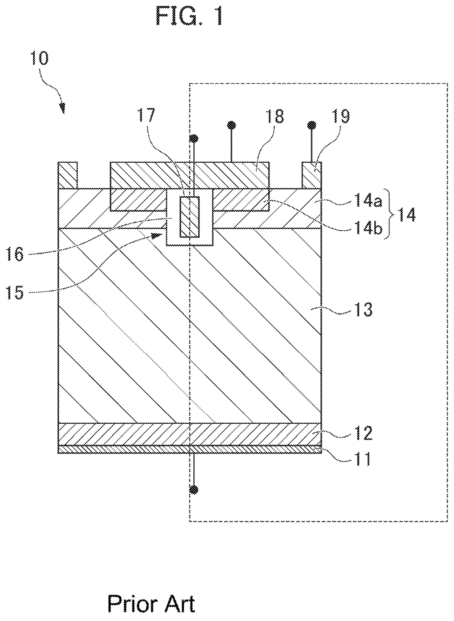
shows a conventional n-channel BiMOS semiconductor device having a trench gate structure.
The BiMOS semiconductor device 10 includes a collector/drain electrode 11 , and an n + drain layer 12 , an n − drift layer 13 , and a composite layer 14 including a p base layer 14 a and an n + source layer 14 b , which are provided in order on the collector/drain electrode 11 . The BiMOS semiconductor device 10 has a trench 15 , which extends from the surface of the composite layer 14 to a top portion of the n − drift layer 13 , and further includes a gate insulating film 16 and a gate electrode 17 which is provided inside the trench 15 with the gate insulating film 16 disposed between the gate electrode 17 and the wall of the trench 15 . In this structure, the n + source layer 14 b is provided in an upper portion of the composite layer 14 and on each of the two sides of the trench 15 . The BiMOS semiconductor device 10 further includes an emitter/source electrode 18 on the n + source layer 14 b and includes a base electrode 19 that is spaced apart by a given distance from the emitter/source electrode 18 and provided on an n + source layer 14 b -free region of the composite layer 14 .
In , a half cell is indicated by broken lines. Such a half cell is shown in and other drawings for illustrating the BiMOS semiconductor device.
Next, how the BiMOS semiconductor device 10 operates will be explained with reference to . It should be noted that in , the thick lines representing electron and hall currents indicate that the currents are large while the thin lines representing electron and hall currents indicate that the currents are small.
As shown in , an inversion layer 14 c is generated in a portion of the p base layer 14 a in the vicinity of the gate electrode 17 when a gate voltage positive with respect to the emitter/source electrode 18 is applied to the gate electrode 17 while a voltage positive with respect to the emitter/source electrode 18 is applied to the collector/drain electrode 11 . In this state, an electron current 21 a flows from the collector/drain electrode 11 to the emitter/source electrode 18 through the n + drain layer 12 , the n − drift layer 13 , the inversion layer 14 c , and the n + source layer 14 b . When a base current is allowed to flow to the base electrode 19 while a voltage positive with respect to the emitter/source electrode 18 is applied to the collector/drain electrode 11 , electron currents 21 b and 21 c flow and an electron current 21 d flows from the collector/drain electrode 11 to the emitter/source electrode 18 through the n + drain layer 12 , the n − drift layer 13 , the p base layer 14 a , and the n + source layer 14 b . A hall current 22 also flows from the p base layer 14 a to the n − drift layer 13 . In this state, the electron currents 21 b and 21 c flow into the n + source layer 14 b from the lateral and lower sides, respectively.
Unfortunately, the BiMOS semiconductor device 10 has a problem in that, for the purpose of high voltage resistance, the n − drift layer 13 cannot have a high impurity concentration and thus a low current density is provided, because the depletion layer extending in the n − drift layer 13 has the highest field intensity at the interface with the p base layer 14 a.
shows a conventional n-channel IGBT having a trench gate structure.
The IGBT 10 A includes a collector electrode 11 , and a p + collector layer 12 A, an n + collector layer 12 , an n − drift layer 13 , and a composite layer 14 including a p emitter layer 14 a and an n + emitter layer 14 b , which are provided in order on the collector electrode 11 . The IGBT 10 A has a trench 15 , which extends from the surface of the composite layer 14 to a top portion of the n − drift layer 13 , and further includes a gate insulating film 16 and a gate electrode 17 which is provided inside the trench 15 with the gate insulating film 16 disposed between the gate electrode 17 and the wall of the trench 15 . In this structure, the n + emitter layer 14 b is provided on each of the two sides of the trench 15 at an upper portion of the composite layer 14 . The IGBT 10 A further includes an emitter electrode 18 A on the top of the composite layer 14 .
Unfortunately, the IGBT 10 A has a problem in that a built-in voltage of about 0.6 V may increase the on-voltage.
It is an object of the present invention to provide a BiMOS semiconductor device having an improved current density.
An aspect of the present invention is directed to an n-channel BiMOS semiconductor device having a trench gate structure, the n-channel BiMOS semiconductor device including: an n + drain layer; a parallel pn layer including n − drift and p pillar layers joined alternately; a composite layer including a p base layer and an n + source layer, the n + drain layer, the parallel pn layer, and the composite layer being provided in order; a high-resistance layer provided between a portion of the p base layer above the p pillar layer and the n + source layer; and a high-resistance layer provided between the p pillar layer and the p base layer, the p pillar layer having an impurity concentration lower than that of the n − drift layer.
Another aspect of the present invention is directed to a p-channel BiMOS semiconductor device having a trench gate structure, the p-channel BiMOS semiconductor device including: a p + drain layer; a parallel pn layer including p − drift and n pillar layers joined alternately; a composite layer including an n base layer and a p + source layer, the p + drain layer, the parallel pn layer, and the composite layer being provided in order; a high-resistance layer provided between a portion of the n base layer above the n pillar layer and the p + source layer; and a high-resistance layer provided between the n pillar layer and the n base layer, the n pillar layer having an impurity concentration lower than that of the p − drift layer.
The present invention makes it possible to provide a BiMOS semiconductor device having an improved current density.
BRIEF DESCRIPTION OF THE DRAWINGS
is a cross-sectional view showing a conventional n-channel BiMOS semiconductor device having a trench gate structure;
is a view for illustrating how the BiMOS semiconductor device of operates;
is a cross-sectional view showing a conventional n-channel IGBT having a trench gate structure;
is a cross-sectional view showing an example of a BiMOS semiconductor device according to an embodiment of the present invention;
is a view for illustrating how the BiMOS semiconductor device of operates;
is a graph showing the results of simulation of the I-V curves of the BiMOS semiconductor devices of and the IGBT of ;
is a view showing the results of simulation of electron current vectors in the BiMOS semiconductor device (N A =0.3N D ) of ;
is a graph showing the results of simulation of the potential barrier at the A-A′ cross-section in ;
is a graph showing the results of simulation of the electron density at the A-A′ cross-section in ;
is a view for illustrating a complementary method for operating only the MOSFET part in the BiMOS semiconductor device of ;
is a view for illustrating a complementary method for operating only the bipolar transistor part in the BiMOS semiconductor device of ;
is a timing chart for illustrating an exemplary way to operate the MOSFET part and the bipolar transistor part independently in the BiMOS semiconductor device of ;
is a view for illustrating other exemplary ways to operate the MOSFET part and the bipolar transistor part independently in the BiMOS semiconductor device of ; and
is a cross-sectional view showing another example of the BiMOS semiconductor device according to the present embodiment.
DETAILED DESCRIPTION OF THE INVENTION
Hereinafter, embodiments of the present invention will be described with reference to the drawings.
shows an exemplary BiMOS semiconductor device according to an embodiment of the present invention.
The BiMOS semiconductor device 30 is an n-channel BiMOS semiconductor device having a trench gate structure.
The BiMOS semiconductor device 30 includes a collector/drain electrode 31 , an n + drain layer 32 , a parallel pn layer 33 including an n − drift layer 33 a and a p pillar layer 33 b joined alternately, and a composite layer 34 including a p base layer 34 a and an n + source layer 34 b , in which the n + drain layer 32 , the parallel pn layer 33 , and the composite layer 34 are provided in order on the collector/drain electrode 31 . The BiMOS semiconductor device 30 has a trench 35 extending from the surface of the composite layer 34 to a top portion of the parallel pn layer 33 , and further includes a gate insulating film 36 and a gate electrode 37 that is provided inside the trench 35 with the gate insulating film 36 disposed between the gate electrode 37 and the wall of the trench 35 . In this structure, the n + source layer 34 b is provided in an upper portion of the composite layer 34 and on each of the two sides of the trench 35 and provided above the n − drift layer 33 a . The BiMOS semiconductor device 30 further includes an emitter/source electrode 38 on the n + source layer 34 b and includes a base electrode 39 that is spaced apart by a given distance from the emitter/source electrode 38 and provided on an n + source layer 34 b -free region of the composite layer 34 .
In the BiMOS semiconductor device 30 , the parallel pn layer 33 allows the depletion layer extending in the n − drift layer 33 a to have an almost uniform field intensity in the thickness direction and thus allows the n − drift layer 33 a to have a high impurity concentration, which allows the BiMOS semiconductor device 30 to have an improved current density.
The BiMOS semiconductor device 30 further includes a high-resistance layer 51 provided between a portion of the p base layer 34 a above the p pillar layer 33 b and the n + source layer 34 b . The high-resistance layer 51 can reduce the electron current flowing from the lateral side to the n + source layer 34 b when the base current is allowed to flow to the base electrode 39 , which allows the BiMOS semiconductor device 30 to have an improved current density.
The BiMOS semiconductor device 30 further includes a high-resistance layer 52 provided between the p pillar layer 33 b and the p base layer 34 a . The high-resistance layer 52 can reduce the electron current flowing from the p base layer 34 a to the n − drift layer 33 a through the p pillar layer 33 b , which allows the BiMOS semiconductor device 30 to have an improved current density.
The high-resistance layers 51 and 52 may be made of SiO 2 as a non-limiting example. The high-resistance layers 51 and 52 are a mode for increasing the resistance of the interlayer portion. Alternatively, high-resistance films may be used in place of the SiO 2 films or other insulating films. Other methods for increasing the resistance of the interlayer portion may be, but not limited to, spatial isolation between the layers.
In this case, the impurity concentration N D of the n − drift layer 33 a and the impurity concentration N A of the p pillar layer 33 b satisfy the formula: N A <N D , This lowers the potential barrier at the interface between the n − drift layer 33 a and the p pillar layer 33 b and thus allows the electron current to easily flow from the n − drift layer 33 a to the p pillar layer 33 b.
The width W D of the n − drift layer 33 a and the width W A of the p pillar layer 33 b also satisfy the formula: W D <W A In this case, W A may be adjusted as appropriate in view of voltage resistance.
The substrate material for the BiMOS semiconductor device 30 is typically, but not limited to, Si, SiC, GaN, Ga 2 O 3 , or any other semiconductor material. The impurities may be a known acceptor and a known donor.
Next, how the BiMOS semiconductor device 30 operates will be explained with reference to . It should be noted that in , the thick lines representing electron and hall currents indicate that the currents are large while the thin lines representing electron and hall currents indicate that the currents are small.
As shown in , an inversion layer 34 c is generated in a portion of the p base layer 34 a in the vicinity of the gate electrode 37 when a gate voltage positive with respect to the emitter/source electrode 38 is applied to the gate electrode 37 while a voltage positive with respect to the emitter/source electrode 38 is applied to the collector/drain electrode 31 . In this state, an electron current 41 a flows from the collector/drain electrode 31 to the emitter/source electrode 38 through the n + drain layer 32 , the n − drift layer 33 a , the inversion layer 34 c , and the n + source layer 34 b.
When a base current is allowed to flow to the base electrode 39 while a voltage positive with respect to the emitter/source electrode 38 is applied to the collector/drain electrode 31 , an electron current 41 c flows from the p base layer 34 a to the n + source layer 34 b . An electron current 41 d also flows from the collector/drain electrode 31 to the emitter/source electrode 38 through the n + drain layer 32 , the n − drift layer 33 a , the p base layer 34 a , and the n + source layer 34 b . A hall current 42 also flows from the p base layer 34 a to the n − drift layer 33 a . In this case, the electron current 41 c flows into the n + source layer 34 b from the lower side.
In this case, since the potential barrier is low at the interface between the n-drift layer 33 a and the p pillar layer 33 b , an electron current 41 f flows from a part of the n − drift layer 33 a to another part of the n − drift layer 33 a through the p pillar layer 33 b.
shows the results of simulation of the I-V curves of the BiMOS semiconductor devices 10 and 30 (see ) and the IGBT 10 A (see ).
indicates that the BiMOS semiconductor device 30 has a current density higher than that of the BiMOS semiconductor device 10 or the IGBT 10 A. It is also apparent that the BiMOS semiconductor device 30 has a higher current density when N A equals 0.3N D or 0.5N D (N A =0.3N D or 0.5N D ) than when N A equals N D (N A =N D ).
In , the I-V curves are the results of the simulation, in which the voltage is applied to the collector/drain electrode 31 , and the current density is the density of the current flowing to the collector/drain electrode 31 .
shows the results of simulation of the electron current vectors in the BiMOS semiconductor device (N A =0.3N D ) of .
As shown in , the electron current 41 f (see ) flows in the p pillar layer 33 b and then flows into the n-drift layer 33 a.
In this case, the lower the potential barrier at the interface between the n − drift layer 33 a and the p pillar layer 33 b , the more easily the electron current 41 f flows into the p pillar layer 33 b from the n − drift layer 33 a . The potential barrier Φ B is expressed by the equation below. The Φ B decreases with decreasing N A .
Φ B = k B T q log ( N A N D n i 2 ) [ Math . 1 ]
In the equation, k B is Boltzmann constant, T is absolute temperature, q is elementary charge, N A is the impurity concentration of the p pillar layer 33 b , N D is the impurity concentration of the n − drift layer 33 a , and n i is intrinsic carrier concentration.
shows the results of simulation of the potential barrier at the A-A′ cross-section in .
indicates that the potential barrier at the interface between the n − drift layer 33 a and the p pillar layer 33 b is lower when N A equals 0.3N D or 0.5N D (N A =0.3N D or 0.5N D ) than when N A equals N D (N A =N D ).
shows the results of simulation of the electron density at the A-A′ cross-section in .
indicates that the electron density at the interface between the n − drift layer 33 a and the p pillar layer 33 b is higher when N A equals 0.3N D or 0.5N D (N A =0.3N D or 0.5N D ) than when N A equals N D (N A =N D ).
Accordingly, when N A =0.3N D or 0.5N D , the potential barrier at the interface between the n − drift layer 33 a and the p pillar layer 33 b in the BiMOS semiconductor device 30 is lower and the electron current 41 f more easily flows into the p pillar layer 33 b than when N A =N D , and the p pillar layer 33 b is more effectively utilized as a route for the electron current 41 f.
In the BiMOS semiconductor device 30 , only the MOSFET part can be operated by voltage-only driving (see ), and only the bipolar transistor part can be operated by current-only driving (see ).
shows an exemplary way to operate the MOSFET part and the bipolar transistor part independently in the BiMOS semiconductor device 30 .
First, at timing A, the gate voltage is switched from Low (L) to High (H) to turn on the MOSFET so that the drain current increases while the drain voltage decreases. Next, at timing B, the base current is switched from L to H to turn on the bipolar transistor, so that at timing C, the drain current increases while the drain voltage decreases. Next, at timing D, the base current is switched from H to L to turn off the bipolar transistor, so that after the elapse of a given period of time, the drain current decreases while the drain voltage increase. Next, at timing E, the gate voltage is switched from H to L to turn off the MOSFET so that the drain current decreases while the drain voltage increases, which results in return to the initial state.
In this case, the bipolar transistor has secondary breakdown limitation in the safe operating area. It is preferred therefore that as shown in , turning off the bipolar transistor should be followed by turning off the MOSFET taking into account bipolar transistor operation delay.
shows other exemplary ways to operate the MOSFET part and the bipolar transistor part independently in the BiMOS semiconductor device 30 . In , I represents the method shown in .
While the BiMOS semiconductor device according to the embodiment has been described with reference to an n-channel BiMOS semiconductor device, the BiMOS semiconductor device according to the embodiment is not limited to an n-channel type and may also be a p channel type.
shows another exemplary BiMOS semiconductor device according to the embodiment.
The BiMOS semiconductor device 60 is a p-channel BiMOS semiconductor device having a trench gate structure.
The BiMOS semiconductor device 60 includes a collector/drain electrode 61 , a p + drain layer 62 , a parallel pn layer 63 including a p − drift layer 63 a and an n pillar layer 63 b joined alternately, and a composite layer 64 including an n base layer 64 a and a p + source layer 64 b , in which the p + drain layer 62 , the parallel pn layer 63 , and the composite layer 64 are provided in order on the collector/drain electrode 61 . The BiMOS semiconductor device 60 has a trench 65 extending from the surface of the composite layer 64 to a top portion of the parallel pn layer 63 , and further includes a gate insulating film 66 and a gate electrode 67 that is provided inside the trench 65 with the gate insulating film 66 disposed between the gate electrode 67 and the wall of the trench 65 . In this structure, the p + source layer 64 b is provided in an upper portion of the composite layer 64 and on each of the two sides of the trench 65 and provided above the p − drift layer 63 a . The BiMOS semiconductor device 60 further includes an emitter/source electrode 68 on the p + source layer 64 b and includes a base electrode 69 that is spaced apart by a given distance from the emitter/source electrode 68 and provided on a p + source layer 64 b -free region of the composite layer 64 .
In the BiMOS semiconductor device 60 , the parallel pn layer 63 allows the depletion layer extending in the p − drift layer 63 a to have an almost uniform field intensity in the thickness direction and thus allows the p − drift layer 63 a to have a high impurity concentration, which allows the BiMOS semiconductor device 60 to have an improved current density.
The BiMOS semiconductor device 60 further includes a high-resistance layer 81 provided between a portion of the n base layer 64 a above the n pillar layer 63 b and the p + source layer 64 b . The high-resistance layer 81 can reduce the electron current flowing from the lateral side to the p + source layer 64 b when the base current is allowed to flow to the base electrode 69 , which allows the BiMOS semiconductor device 60 to have an improved current density.
The BiMOS semiconductor device 60 further includes a high-resistance layer 82 provided between the n pillar layer 63 b and the n base layer 64 a . The high-resistance layer 82 can reduce the electron current flowing from the n base layer 64 a to the p − drift layer 63 a through the n pillar layer 63 b , which allows the BiMOS semiconductor device 60 to have an improved current density.
The high-resistance layers 81 and 82 may be made of SiO 2 as a non-limiting example. The high-resistance layers 81 and 82 are a mode for increasing the resistance of the interlayer portion. Alternatively, high-resistance films may be used in place of the SiO 2 films or other insulating films. Other methods for increasing the resistance of the interlayer portion may be, but not limited to, spatial isolation between the layers.
In this case, the impurity concentration N h of the p − drift layer 63 a and the impurity concentration N n of the n pillar layer 63 b satisfy the formula: N D <N A This lowers the potential barrier at the interface between the p − drift layer 63 a and the n pillar layer 63 b and thus allows the hall current to easily flow from the p − drift layer 63 a to the n pillar layer 63 b.
The width W A of the p − drift layer 63 a and the width W D of the n pillar layer 63 b also satisfy the formula: W A <W D In this case, W D may be adjusted as appropriate in view of voltage resistance.
The substrate material for the BiMOS semiconductor device 60 is typically, but not limited to, Si, SiC, GaN, Ga 2 O 3 or any other semiconductor material. The impurities may be a known acceptor and a known donor.
Next, how the BiMOS semiconductor device 60 operates will be explained. It should be noted that in , the thick lines representing electron and hall currents indicate that the currents are large while the thin lines representing electron and hall currents indicate that the currents are small.
As shown in , an inversion layer 64 c is generated in a portion of the n base layer 64 a in the vicinity of the gate electrode 67 when a gate voltage negative with respect to the emitter/source electrode 68 is applied to the gate electrode 67 while a voltage negative with respect to the emitter/source electrode 68 is applied to the collector/drain electrode 61 . In this state, a hall current 71 a flows from the emitter/source electrode 68 to the collector/drain electrode 61 through the p + drain layer 62 , the p − drift layer 63 a , the inversion layer 64 c , and the p + source layer 64 b . When a base current is allowed to flow from the base electrode 69 while a voltage negative with respect to the emitter/source electrode 68 is applied to the collector/drain electrode 61 , a hall current 71 c flows from the p + source layer 64 b to the n base layer 64 a . A hall current 71 d also flows from the emitter/source electrode 68 to the collector/drain electrode 61 through the p + drain layer 62 , the p − drift layer 63 a , the n base layer 64 a , and the p + source layer 64 b . An electron current 72 also flows from the p − drift layer 63 a to the n base layer 64 a . In this state, the hall current 71 c flows into the n base layer 64 a from the lower side.
In this case, since the potential barrier is low at the interface between the p − drift layer 63 a and the n pillar layer 63 b , a hall current 71 f flows from a part of the p − drift layer 63 a to another part of the p − drift layer 63 a through the n pillar layer 63 b.
EXPLANATION OF REFERENCE NUMERALS
•
• 10 : BiMOS semiconductor device • 10 A: IGBT • 11 : Collector/drain electrode (collector electrode) • 12 : n + drain layer (n + collector layer) • 12 A: p + collector layer • 13 : n − drift layer • 14 : Composite layer • 14 a : p base layer (p emitter layer) • 14 b : n + source layer (n + emitter layer) • 14 c : Inversion layer • 15 : Trench • 16 : Gate insulating film • 17 : Gate electrode • 18 : Emitter/source electrode • 18 A: Emitter electrode • 19 : Base electrode • 21 a , 21 b , 21 c , 21 d : Electron current • 22 : Hall current • 30 : BiMOS semiconductor device • 31 : Collector/drain electrode • 32 : n + drain layer • 33 : Parallel pn layer • 33 a : n − drift layer • 33 b : p pillar layer • 34 : Composite layer • 34 a : p base layer • 34 b : n + source layer • 34 c : Inversion layer • 35 : Trench • 36 : Gate insulating film • 37 : Gate electrode • 38 : Emitter/source electrode • 39 : Base electrode • 41 a , 41 c , 41 d , 41 f : Electron current • 42 : Hall current • 51 , 52 : High-resistance layer • 60 : BiMOS semiconductor device • 61 : Collector/drain electrode • 62 : p + drain layer • 63 : Parallel pn layer • 63 a : p − drift layer • 63 b : n pillar layer • 64 : Composite layer • 64 a : n base layer • 64 b : p + source layer • 64 c : Inversion layer • 65 : Trench • 66 : Gate insulating film • 67 : Gate electrode • 68 : Emitter/source electrode • 69 : Base electrode • 71 a , 71 c , 71 d , 71 f : Hall current • 72 : Electron current • 81 , 82 : High-resistance layer
Figures (13)
Citations
This patent cites (12)
- US4941030
- US20070181927
- US20170047319
- US20170221989
- US20200152748
- US20200235203
- USS60196974
- USS61180472
- USS61225854
- US2015039010
- US2020077800
- US2019069416