Display Device, Detecting Method and Pixel Driving Circuit
Abstract
A display device includes a light emitting unit, first and second capacitors, and first and second switches. The light emitting unit emits light according to a voltage level of a first node. A first terminal of the first capacitor is coupled to the first node, and a second terminal of the first capacitor is coupled to a second node. A first terminal of the second capacitor is coupled to the second node, and a second terminal of the first capacitor is coupled to the light emitting unit. A first terminal of the first switch is coupled to the first node, and a second terminal of the first switch is coupled to the light emitting unit. The second switch is configured to be turned on before the first switch is turned on, and a first terminal of the second switch is coupled to the first node.
Claims (20)
1. A display device, comprising pixel driving circuits coupled to each other in series, one of the pixel driving circuits comprising: a light emitting unit configured to emit light according to a voltage level of a first node; a first capacitor, a first terminal of the first capacitor being coupled to the first node, and a second terminal of the first capacitor being coupled to a second node; a second capacitor, a first terminal of the second capacitor being coupled to the second node, and a second terminal of the first capacitor being coupled to the light emitting unit; a first switch, a first terminal of the first switch being coupled to the first node, and a second terminal of the first switch being coupled to the light emitting unit; and a second switch configured to be turned on before the first switch is turned on, a first terminal of the second switch being coupled to the first node, wherein the first switch is configured to adjust a voltage level of the first node according to a scan signal which is received by a control terminal of the first switch, and the control terminal of the first switch is different from the first terminal of the first switch.
7. A detecting method, comprising: writing a first reference signal through a first switch into a control terminal of the first switch at a first node; after writing the first reference signal into the control terminal of the first switch, writing a data signal through a first capacitor into the first node; generating a first current flowing through the first switch; measuring the first current; and determining the first switch being normal, in response to a current level the first current corresponding to the data signal, wherein writing the first reference signal comprises writing the first reference signal through a first terminal of the first switch and a second terminal of the first switch in order, and the control terminal of the first switch, the first terminal of the first switch and the second terminal of the first switch are different from each other.
16. A pixel driving circuit comprising: a first switch configured to generate a current according to a voltage level of a first node, a control terminal of the first switch being coupled to the first node; and a second switch, a first terminal of the second switch being coupled to the first node, a second terminal of the second switch being coupled to a first terminal of the first switch at a second node; a third switch, a control terminal of the third switch being configured to receive a light emitting signal, a first terminal of the third switch being coupled to the second node; a fourth switch, a control terminal of the fourth switch being configured to receive the light emitting signal, a first terminal of the third switch being coupled to a second terminal of the first switch at a third node; a light emitting element configured to receive the current to emit light; and a data writing unit coupled to the first node and the third node, and configured to adjust the voltage level of the first node, wherein the first switch is configured to adjust a voltage level of the first node according to a scan signal which is received by a control terminal of the first switch, and the control terminal of the first switch is different from the first terminal of the first switch.
Show 17 dependent claims
2. The display device of claim 1 , further comprising: a third switch configured to be turned on when the second switch is turned on, a first terminal of the third switch being coupled to the second node.
3. The display device of claim 2 , wherein the third switch is further configured to be turned off when the second switch is turned off.
4. The display device of claim 2 , further comprising: a fourth switch configured to be turned on when the second switch and the third switch are turned off, a first terminal of the fourth switch being coupled to the second node.
5. The display device of claim 2 , wherein a second terminal of the second switch and a second terminal of the third switch are configured to receive a reference signal.
6. The display device of claim 5 , further comprising: a fourth switch configured to provide the reference signal to the second node when the second switch and the third switch are turned off.
8. The detecting method of claim 7 , further comprising: determining the first switch being abnormal, in response to the current level not corresponding to the data signal.
9. The detecting method of claim 7 , further comprising: determining a second switch being normal, in response to the current level corresponding to the data signal, wherein writing the first reference signal further comprises: writing the first reference signal through the first switch and the second switch in order, wherein the first terminal of the first switch is coupled to a first terminal of the second switch, a second terminal of the second switch is coupled to the control terminal of the first switch at the first node.
10. The detecting method of claim 7 , further comprising: determining a second switch being normal, in response to the current level corresponding to the data signal; and after measuring the first current, coupling a light emitting element to an accommodating space positioned between a second node and a third node, wherein the first switch and the second switch are configured to generate a second current passing through the second node and the third node, after the light emitting element is coupled to the accommodating space.
11. The detecting method of claim 10 , further comprising: turning on the second switch and a third switch simultaneously, to generate the second current; and receiving the second current by the light emitting element, wherein a first terminal of the third switch is coupled to the first terminal of the first switch.
12. The detecting method of claim 11 , further comprising: determining the third switch being normal, in response to a brightness of the light emitting element corresponding to the data signal, when the light emitting element receives the second current.
13. The detecting method of claim 10 , further comprising: generating a third current by a third switch; and determining the third switch being normal, in response to a brightness of the light emitting element corresponding to a voltage level of a voltage signal, when the light emitting element receives the third current, wherein a first terminal of the third switch is coupled to the first terminal of the first switch, and a second terminal of the third switch is configured to receive the voltage signal.
14. The detecting method of claim 10 , wherein generating the first current comprises: generating the first current flowing through the first switch, the second switch and a third switch in order, to a third node, and writing the data signal comprises: writing the data signal through the second node, a fourth switch and the first capacitor in order, into the first node.
15. The detecting method of claim 14 , wherein generating the first current comprises: generating the first current flowing through the first switch, the second switch, the third switch and the fourth switch in order, to the third node.
17. The pixel driving circuit of claim 16 , further comprising: a fifth switch, a first terminal of the fifth switch being coupled to a second terminal of the third switch and the light emitting element, a second terminal of the fifth switch being coupled to the data writing unit.
18. The pixel driving circuit of claim 17 , wherein the data writing unit comprises: a first capacitor coupled between a fifth node and the first node; and a sixth switch, a first terminal of the sixth switch being coupled to the fifth node.
19. The pixel driving circuit of claim 18 , wherein the second terminal of the fifth switch is coupled to the fifth node or a second terminal of the sixth switch.
20. The pixel driving circuit of claim 16 , wherein the light emitting element being coupled to a second terminal of the fourth switch.
Full Description
Show full text →
CROSS-REFERENCE TO RELATED APPLICATION
This application is a continuation application of U.S. application Ser. No. 17/203,792, filed on Mar. 17, 2021, which claims priority to Taiwan Application Serial Number 109146954, filed Dec. 30, 2020, which is herein incorporated by reference in its entirety.
BACKGROUND
Technical Field
The present disclosure relates to display technology. More particularly, the present disclosure relates to a display device, a detecting method and a pixel driving circuit.
Description of Related Art
During manufacturing processes, pixel driving circuits on a substrate of a display device may suffer from metal residue and excessive etching which cause substrate abnormalities. Manufacturing processes of light emitting elements, such as micro light emitting diodes, are complicated, resulting in higher costs. In addition, currents in conventional pixel driving circuits may be affected by the characteristics of switches and/or resistance on current paths which cause non-uniform brightness of a display.
SUMMARY
The present disclosure provides a display device. The display device includes pixel driving circuits coupled to each other in series. One of the pixel driving circuits includes a light emitting unit, first and second capacitors, and first and second switches. The light emitting unit emits light according to a voltage level of a first node. A first terminal of the first capacitor is coupled to the first node, and a second terminal of the first capacitor is coupled to a second node. A first terminal of the second capacitor is coupled to the second node, and a second terminal of the first capacitor is coupled to the light emitting unit. A first terminal of the first switch is coupled to the first node, and a second terminal of the first switch is coupled to the light emitting unit. The second switch is configured to be turned on before the first switch is turned on, and a first terminal of the second switch is coupled to the first node.
The present disclosure provides a detecting method. The detecting method includes: writing a first reference signal through a first switch into a control terminal of the first switch at a first node; after writing the first reference signal into the control terminal of the first switch, writing a data signal through a first capacitor into the first node; generating a first current flowing through the first switch; measuring the first current; and determining the first switch being normal, in response to a current level the first current corresponding to the data signal.
The present disclosure provides a pixel driving circuit. The pixel driving circuit includes a first switch, a second switch, a third switch, a fourth switch, a light emitting element and a data writing unit. The first switch is configured to generate a current according to a voltage level of a first node, a control terminal of the first switch is coupled to the first node. A first terminal of the second switch is coupled to the first node, a second terminal of the second switch is coupled to a first terminal of the first switch at a second node. A control terminal of the third switch is configured to receive a light emitting signal, a first terminal of the third switch is coupled to the second node. A control terminal of the fourth switch is configured to receive the light emitting signal, a first terminal of the third switch is coupled to a second terminal of the first switch at a third node. The light emitting element is configured to receive the current to emit light. The data writing unit is coupled to the first node and the third node, and is configured to adjust the voltage level of the first node.
It is to be understood that both the foregoing general description and the following detailed description are by examples, and are intended to provide further explanation of the disclosure as claimed.
BRIEF DESCRIPTION OF THE DRAWINGS
Aspects of the present disclosure are best understood from the following detailed description when read with the accompanying figures. It is noted that, in accordance with the standard practice in the industry, various features are not drawn to scale. In fact, the dimensions of the various features may be arbitrarily increased or reduced for clarity of discussion.
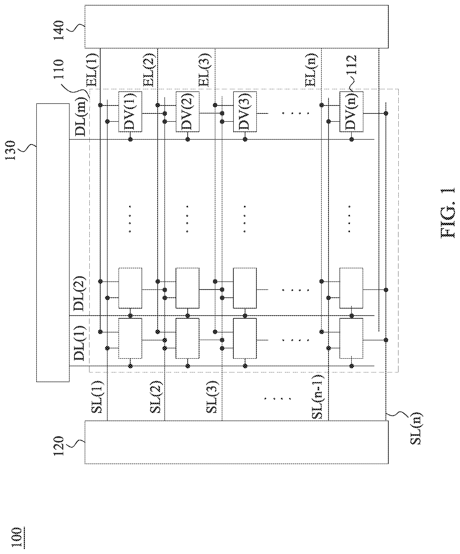
is a schematic diagram of a display according to one embodiment of this disclosure.
is a circuit diagram of a pixel driving circuit in a display device according to one embodiment of this disclosure.
is a timing diagram of the pixel driving circuit performing a driving operation according to one embodiment of this disclosure.
is a timing diagram of the pixel driving circuit performing a driving operation according to one embodiment of this disclosure.
is a circuit diagram of the pixel driving circuit in the display device according to one embodiment of this disclosure.
is a circuit diagram of the pixel driving circuit in the display device according to one embodiment of this disclosure.
is a timing diagram of the pixel driving circuit performing a detecting operation according to one embodiment of this disclosure.
is a circuit diagram of the pixel driving circuit in the display device according to one embodiment of this disclosure.
is a timing diagram of the pixel driving circuit performing a detecting operation according to one embodiment of this disclosure.
is a timing diagram of the pixel driving circuit performing a detecting operation according to one embodiment of this disclosure.
DETAILED DESCRIPTION
The following disclosure provides many different embodiments, or examples, for implementing different features of the provided subject matter.
Specific examples of components and arrangements are described below to simplify the present disclosure. These are, of course, merely examples and are not intended to be limiting. For example, the formation of a first feature over or on a second feature in the description that follows may include embodiments in which the first and second features are formed in direct contact, and may also include embodiments in which additional features may be formed between the first and second features, such that the first and second features may not be in direct contact. In addition, the present disclosure may repeat reference numerals and/or letters in the various examples. This repetition is for the purpose of simplicity and clarity and does not in itself dictate a relationship between the various embodiments and/or configurations discussed.
Further, spatially relative terms, such as “beneath,” “below,” “lower,” “above,” “upper” and the like, may be used herein for ease of description to describe one element or feature's relationship to another element(s) or feature(s) as illustrated in the figures. The spatially relative terms are intended to encompass different orientations of the device in use or operation in addition to the orientation depicted in the figures. The apparatus may be otherwise oriented (rotated 90 degrees or at other orientations) and the spatially relative descriptors used herein may likewise be interpreted accordingly.
The terms applied throughout the following descriptions and claims generally have their ordinary meanings clearly established in the art or in the specific context where each term is used. Those of ordinary skill in the art will appreciate that a component or process may be referred to by different names. Numerous different embodiments detailed in this specification are illustrative only, and in no way limit the scope and spirit of the disclosure or of any exemplified term.
It is worth noting that terms such as “first” and “second” used herein to describe various elements or processes aim to distinguish one element or process from another. However, the elements, processes and the sequences thereof should not be limited by these terms. For example, a first element could be termed as a second element, and a second element could be similarly termed as a first element without departing from the scope of the present disclosure.
In the following discussion and in the claims, the terms “comprising,” “including,” “containing,” “having,” “involving,” and the like are to be understood to be open-ended, that is, to be construed as including but not limited to. As used herein, instead of being mutually exclusive, the term “and/or” includes any of the associated listed items and all combinations of one or more of the associated listed items.
Reference will now be made in detail to the present embodiments of the disclosure, examples of which are illustrated in the accompanying drawings. Wherever possible, the same reference numbers are used in the drawings and the description to refer to the same or like parts.
is a schematic diagram of a display according to one embodiment of this disclosure. As illustratively shown in , a display 100 includes a display device 110 , a scan device 120 , a data input device 130 and a light emitting controlling device 140 . The scan device 120 is configured to provide scan signals, such as scan signals S(n−2), S(n−1) and S(n) shown in , to the display device 110 by scan lines SL( 0 )-SL(n). The data input device 130 is configured to provide data signals, such as a data signal DT shown in , to the display device 110 by data lines DL( 0 )-DL(m). The light emitting controlling device 140 is configured to provide light emitting signals, such as a light emitting signal EM shown in , to the display device 110 by light emitting lines EL( 0 )-EL(n). It is noted that n and m are positive integers. In some embodiments, the display 100 can be manufactured by a glass substrate or a plastic substrate, but the present disclosure is not limited to such embodiments.
As illustratively shown in , the display device 110 includes multiple stages of pixel driving circuits DV( 1 )-DV(n) coupled in series with each other. The pixel driving circuits DV( 1 )-DV(n) include a pixel driving circuit 112 . In some embodiments, the pixel driving circuit 112 included in the display device 110 performs a light emitting operation according to the signals provided by the scan device 120 , the data input device 130 and the light emitting controlling device 140 .
For example, a pixel driving circuit 200 shown in is an embodiment of the pixel driving circuit 112 . As illustratively shown in , the pixel driving circuit 200 is reset by the scan signals S(n−2), S(n−1) and S(n) provided by the scan device 120 , and writes the data signal DT provided by the data input device 130 . A voltage level of the data signal DT determines a brightness of the light emitting element L 2 . A light emitting duration of the light emitting element L 2 is controlled by the light emitting signal EM provided by the light emitting controlling device 140 .
In some embodiments, the scan signals S(n−1) and S(n) are transmitted to the pixel driving circuit 112 through the scan lines SL(n−1) and SL(n), respectively. The data signal DT is transmitted to the pixel driving circuit 112 through the data line DL(m). The light emitting signal EM is transmitted to the pixel driving circuit 112 through the light emitting line EL(n). The present disclosure is not limited to the embodiments described above. Various methods of transmitting the scan signals S(n−1), S(n), the data signal DT and the light emitting signal EM are contemplated as being within the scope of the present disclosure.
is a circuit diagram of the pixel driving circuit 200 in the display device 110 according to one embodiment of this disclosure. The pixel driving circuit 200 is an embodiment of the pixel driving circuit 112 in the display device 110 .
As illustratively shown in , the pixel driving circuit 200 includes a reset unit 210 , a data writing unit 220 , a compensation unit 230 , light emitting unit 240 and a stabilizing unit 250 .
As illustratively shown in , the reset unit 210 is configured to perform a reset operation according to the scan signal S(n−2), to reset voltage levels of nodes N 21 and N 22 . In other embodiments, such as the embodiment illustratively shown in , the reset unit 210 is further configured to perform a reset operation according to a voltage signal SLT.
As illustratively shown in , the data writing unit 220 is configured to perform a data writing operation according to the scan signal S(n), to write the data signal DT into the node N 21 .
As illustratively shown in , the compensation unit 230 is configured to adjust a voltage level of the node N 22 according to the scan signal S(n−1). For example, the compensation unit 230 writes a threshold voltage level V TH into the node N 22 to perform a compensating operation.
As illustratively shown in , the light emitting unit 240 is configured to perform a light emitting operation according to the light emitting signal EM, generate a current I 2 according to the voltage level of the node N 22 , and emit light according to a current level of the current I 2 .
As illustratively shown in , the stabilizing unit 250 is configured to transmit a reference signal VRF 2 to a node N 23 according to the light emitting signal EM, to reset a voltage level of the node N 23 and stabilize the voltage level of the node N 21 .
In some embodiments, the pixel driving circuit 200 is an nth stage pixel driving circuit DV(n) of the pixel driving circuits in the display 100 . Accordingly, the scan signal S(n) is an nth stage scan signal, the scan signal S(n−1) is an (n−1)th stage scan signal, and the scan signal S(n−2) is an (n−2)th stage scan signal. An (n−1)th stage pixel driving circuit DV(n−1) of the pixel driving circuits in the display 100 is configured to perform a data writing operation according to the scan signal S(n−1). An (n−2)th stage pixel driving circuit DV(n−1) in the display 100 is configured to perform a data writing operation according to the scan signal S(n−2).
As illustratively shown in , the reset unit 210 includes switches T 25 and T 26 . A control terminal of the switch T 26 is configured to receive the scan signal S(n−2), a terminal of the switch T 26 is coupled to the node N 22 , and another terminal of the switch T 26 is configured to receive a reference signal VRF 1 . A terminal of the switch T 25 is coupled to the node N 21 , and another terminal of the switch T 25 is configured to receive the reference signal VRF 1 . In different embodiments, a control terminal of the switch T 25 is configured to receive the scan signal S(n−2) (corresponding to the embodiment shown in ) or a voltage signal SLT (corresponding to the embodiment shown in ).
As illustratively shown in , the data writing unit 220 includes a switch T 21 , and capacitors C 21 and C 22 . A control terminal of the switch T 21 is configured to receive the scan signal S(n), a terminal of the switch T 21 is configured to receive the data signal DT, and another terminal of the switch T 21 is coupled to the node N 21 . A terminal of the capacitor C 21 is coupled to the node N 21 , and another terminal of the capacitor C 21 is coupled to the node N 22 . A terminal of the capacitor C 22 is coupled to the node N 21 , and another terminal of the capacitor C 22 is coupled to the node N 23 .
As illustratively shown in , the compensation unit 230 includes a switch T 24 . A control terminal of the switch T 24 is configured to receive the scan signal S(n−1), a terminal of the switch T 24 is coupled to the node N 22 , and another terminal of the switch T 24 is coupled to the light emitting unit 240 at a node N 24 .
As illustratively shown in , the light emitting unit 240 includes the light emitting element L 2 , and switches T 22 , T 23 and T 27 . A control terminal of the switch T 22 is coupled to the node N 22 , a terminal of the switch T 22 is coupled to the node N 24 , and another terminal of the switch T 22 is coupled to the node N 23 . A control terminal of the switch T 23 is configured to receive the light emitting signal EM, a terminal of the switch T 23 is coupled to the node N 24 , and another terminal of the switch T 23 is configured to receive a voltage signal VSS. A control terminal of the switch T 27 is configured to receive the light emitting signal EM, a terminal of the switch T 27 is coupled to the light emitting element L 2 at a node N 25 , and another terminal of the switch T 27 is coupled to the node N 23 . A terminal of the light emitting element L 2 is coupled to the node N 25 , and another terminal of the light emitting element L 2 is configured to receive a voltage signal VDD. In some embodiments, the light emitting element L 2 is configured to receive the current I 2 passing through the switch T 22 , and configured to emit light according to the current I 2 .
As illustratively shown in , the stabilizing unit 250 includes a switch T 28 . A control terminal of the switch T 28 is configured to receive a control signal VC, a terminal of the switch T 28 is coupled to the node N 23 , and another terminal of the switch T 28 is configured to receive a reference signal VRF 2 .
In different embodiments, the light emitting element L 2 can be implemented by a micro light emitting diode (mLED) or another type of light emitting element. In different embodiments, the switches T 21 -T 28 can be implemented by p-type metal-oxide-semiconductor field-effect transistors (PMOS), n-type metal-oxide-semiconductor field-effect transistors (NMOS), thin film transistors (TFT) or other types of switching elements.
is a timing diagram of the pixel driving circuit 200 performing a driving operation according to one embodiment of this disclosure. The timing diagram illustratively shown in includes periods P 31 -P 34 in order. In some embodiments, the timing diagram shown in corresponds to signals shown in , such as operations of the scan signals S(n−2), S(n−1) and S(n), the light emitting signal EM, the data signal DT and the control signal VC. In the embodiment shown in , the control terminal of the switch T 25 is configured to receive the scan signal S(n−2).
As illustratively shown in , during the period P 31 , the control signal VC has an enable voltage level VGL, such that the switches T 25 , T 26 and T 28 are turned on. At this time, the switches T 25 and T 26 provide the reference signal VRF 1 having a voltage level RF 1 to the nodes N 21 and N 22 , respectively, such that the nodes N 21 and N 22 have the voltage level RF 1 . The switch T 28 provides the reference signal VRF 2 having a voltage level RF 2 to the node N 23 , such that the node N 23 has the voltage level RF 2 .
In some embodiments, the voltage level RF 1 is an enable voltage level, such that the switch T 22 is turned on according to the voltage level RF 1 of the node N 21 . In some embodiments, the capacitor C 21 is configured to store charges of the node N 21 to maintain the voltage level of the node N 21 after the switch T 26 is turned off, such that the switch T 22 continues to be turned on after the switch T 26 is turned off, such as during the period P 32 .
In some embodiments, during the period P 31 , the voltage levels of the nodes N 21 , N 22 and N 23 are reset by the reference signals VRF 1 and VRF 2 , such that the pixel driving circuit 200 is prepared to receive the data signal DT, and thus the period P 31 is referred to as a reset period.
During the period P 32 , the scan signal S(n−1) and the control signal VC have the enable voltage level VGL, such that the switches T 24 and T 28 are turned on. The scan signal S(n−2) has a disable voltage level VGH, such that the switches T 25 and T 26 are turned off. The switch T 28 provides the reference signal VRF 2 to the node N 23 , such that the node N 23 has the voltage level RF 2 . Due to the charges stored by the capacitor C 21 during the period P 31 , the node N 22 still has an enable voltage level during the period P 32 , and thus the switch T 22 is turned on during the period P 32 . In some embodiments, the voltage level RF 2 of the reference signal VRF 2 is higher than the voltage level RF 1 of the node N 22 , such that a current flows from the node N 23 , through the switches T 22 and T 24 in order, and to the node N 22 . At this time, the reference signal VRF 2 is written into the node N 22 through the switches T 28 , T 22 and T 24 in order, such that the voltage level of the node N 22 is pulled to (RF 2 −|V TH |), in which the threshold voltage level V TH is the threshold voltage level of the switch T 22 . At this time, the voltage level of the node N 21 is determined by the voltage level RF 2 of the node N 23 , the voltage level (RF 2 −|V TH |) of the node N 22 , and the voltage level RF 1 of the node N 21 during the period P 31 .
As illustratively shown in , the capacitors C 21 and C 22 are coupled to each other in series. During the period P 32 , according to a formula of capacitors coupled in series, the voltage level of the node N 21 can be calculated as (RF 1 +((RF 2 −|V TH |−RF 1 )×(CV 21 /(CV 21 +CV 22 ))). The capacitor values CV 21 and CV 22 are the capacitor values of the capacitors C 21 and C 22 , respectively. In some embodiments, the capacitor value CV 22 is much larger than the capacitor value CV 21 . For example, the capacitor value CV 22 is more than ten times larger than the capacitor value CV 21 . As a result, the term (CV 21 /(CV 21 +CV 22 )) approaches zero, and thus the voltage level of the node N 21 can be considered to be equal to the voltage level RF 1 .
In some embodiments, during the period P 32 , the voltage level of the node N 22 is adjusted to (RF 2 −|V TH |) in preparation of compensating for the threshold voltage level V TH of the switch T 22 during a light emitting period, such as the period P 34 . Accordingly, the period P 32 is referred to as a compensating period.
In some previous approaches, the voltage signal configured to perform compensation is affected by an internal resistance of the circuit element of the pixel driving circuit, and thus suffers from a voltage drop (IR drop), such that the voltage levels of the nodes in the pixel driving circuit are not stable.
Compared to the above approaches, in some embodiments of the present disclosure, the switch T 28 transmits the reference signal VRF 2 which is not affected by an IR drop to the node N 23 , and further stabilizes the voltage level of the node N 21 by the capacitor C 22 .
During the period P 33 , the scan signal S(n) and the control signal VC have the enable voltage level VGL, such that the switches T 21 and T 28 are turned on. The scan signal S(n−1) has a disable voltage level VGH, such that the switch T 24 is turned off. The switch T 28 provides the reference signal VRF 2 to the node N 23 , such that the node N 23 has the voltage level RF 2 . At this time, the switch T 21 writes the data signal DT having a voltage level VDT into the node N 21 , such that the voltage level of the node N 21 is pulled to the voltage level VDT. The capacitor C 21 writes the voltage level VDT of the node N 21 into the node N 22 , to pull the voltage level of the node N 22 to (RF 2 −|V TH |+(VDT−RF 1 )). At this time, a voltage level difference VGS between the nodes N 22 and N 23 is (VDT−RF 1 −|V TH |).
In some embodiments, during the period P 33 , the switch T 21 and the capacitor C 21 write the data signal DT into the node N 22 . Accordingly, the period P 33 is referred to as a data writing period.
During the period P 34 , the light emitting signal EM has the enable voltage level VGL, such that the switches T 23 and T 27 are turned on. The scan signal S(n) and the control signal VC have a disable voltage level VGH, such that the switches T 21 and T 28 are turned off. At this time, the voltage signal VDD having a voltage level DD pulls the voltage level of the node N 23 to (DD−VLED−VT 27 ) through the light emitting element L 2 and the switch T 27 . The voltage level differences VLED and VT 27 correspond to the voltage level differences generated when the voltage signal VDD passes through the light emitting element L 2 and the switch T 27 , respectively. Accordingly, the voltage level of the node N 22 is pulled to (VDT−RF 1 −|V TH |+(DD−VLED−VT 27 )) by the capacitors C 21 and C 22 . At this time, the voltage level difference VGS between the nodes N 22 and N 23 is (VDT−RF 1 −|V TH |).
During the period P 34 , the current I 2 flows through the light emitting element L 2 , and the switches T 27 , T 22 and T 23 in order, such that the light emitting element L 2 emits light according to the current level of the current I 2 . In some embodiments, the current level of the current I 2 determines the brightness of the light emitting element L 2 .
In some embodiments, the current level of the current I 2 is determined by the voltage level difference between a gate terminal and a source terminal of the switch T 22 , which is the voltage level difference VGS between the nodes N 22 and N 23 . It may be determined utilizing formulas in electronics that the current I 2 passing through the switch T 22 has a current level K×(VGS+|V TH |){circumflex over ( )}2. During the period P 34 , the voltage level difference VGS is (VDT−RF 1 −|V TH |). K is a constant. As a result, the current level of the current I 2 is independent from the threshold voltage level V TH , while it is dependent upon the voltage level DT of the data signal DT and the voltage level RF 1 of the reference signal VRF 1 .
In some embodiments, during the period P 34 , the light emitting element L 2 of the pixel driving circuit 200 emits light, and thus the period P 34 is referred to as a light emitting period.
In some previous approaches, when the current passes through different paths in the display, different resistance values on the different paths cause different voltage drops. In addition, the threshold voltage levels of the switches also cause voltage drops. The current passing through the light emitting element is hard to control, such that the brightness of the display is not uniform.
Compared to the above approaches, in some embodiments of the present disclosure, the voltage levels VDT and RF 1 are determined by users. As a result, the current I 2 passing through the light emitting element L 2 can be adjusted by the users, and is therefore prevented from being affected by current paths, or element features of the pixel driving circuit, such as the threshold voltage V TH of the switch T 22 .
In other embodiments, the pixel driving circuit 200 does not perform compensation of the threshold voltage level V TH of the switch T 22 . As described in relation to the operation of the pixel driving circuit 200 during the period P 32 , the voltage level RF 2 of the reference signal VRF 2 is higher than the voltage level RF 1 of the node N 22 , such that the switches T 22 and T 24 perform the compensating operation by writing the threshold voltage level V TH into the node N 22 with the reference signal VRF 2 . In contrast, when the user adjusts the voltage level of the reference signal VRF 2 to be lower than or equal to the voltage level RF 1 , the threshold voltage level V TH is not written into the node N 22 , such that compensation of the threshold voltage level V TH of the switch T 22 does not occur. As a result, during the following period P 34 , the voltage level difference VGS is (VDT−RF 1 ), and the current level of the current I 2 is K×(VDT−RF 1 +|V TH |){circumflex over ( )}2. In different embodiments, the compensating function of the pixel driving circuit 200 can be turned on or turned off by different voltage levels of the reference signal VRF 2 .
is a timing diagram of the pixel driving circuit 200 performing a driving operation according to one embodiment of this disclosure. The timing diagram illustratively shown in includes periods P 41 -P 44 in order. In some embodiments, the timing diagram shown in corresponds to signals shown in , such as operations of the scan signals S(n−2), S(n−1) and S(n), the light emitting signal EM, the voltage signal SLT, the data signal DT and the control signal VC. In the embodiment shown in , the control terminal of the switch T 25 is configured to receive the voltage signal SLT.
Referring to and , operations of the pixel driving circuit 200 during the periods P 41 -P 44 are similar to the operations during the periods P 31 -P 34 , and thus similar aspects of these operations are not repeated for brevity.
As illustratively shown in , during the period P 41 , the voltage signal SLT has an enable voltage level VGL, such that the switch T 25 is turned on. At this time, the switch T 25 provides the reference signal VRF 1 having a voltage level RF 1 to the node N 21 , such that the node N 21 has the voltage level RF 1 .
During the period P 42 , the voltage signal SLT, the scan signal S(n−1) and the control signal VC have the enable voltage level VGL, such that the switches T 25 , T 24 and T 28 are turned on. The scan signal S(n−2) has a disable voltage level VGH, such that the switch T 26 is turned off. The switch T 28 provides the reference signal VRF 2 to the node N 23 , such that the node N 23 has the voltage level RF 2 and the node N 22 has a voltage level (RF 2 −|V TH |). The switch T 25 provides the reference signal VRF 1 having a voltage level RF 1 to the node N 21 , such that the node N 21 has the voltage level RF 1 .
During the period P 43 , when the switch T 21 writes the data signal DT into the node N 21 , the capacitor C 21 writes a voltage level difference between the voltage levels RF 1 and VDT into the node N 22 for the data writing operation. At this time, the voltage level of the node N 22 is (RF 2 −|V TH |+(VDT−RF 1 )).
Referring to and , operations of the switch T 25 receiving the voltage signal SLT during the periods P 43 and P 44 are similar to the operations of the switch T 25 receiving the scan signal S(n−2) during the period P 33 and P 34 , and thus similar aspects of these operations are not repeated for brevity. In different embodiments, the switch T 25 can receive the voltage signal SLT or the scan signal S(n−2) to perform operations.
is a circuit diagram of the pixel driving circuit 500 in the display device 110 according to one embodiment of this disclosure. The pixel driving circuit 500 is an embodiment of the pixel driving circuit 112 in the display device 110 . The pixel driving circuit 500 is an alternative embodiment of the pixel driving circuit 200 illustratively shown in .
As illustratively shown in , the pixel driving circuit 500 includes switches T 51 -T 59 , capacitors C 52 , C 51 and a light emitting element L 5 . Referring to and , the configuration of the pixel driving circuit 500 is similar to that of the pixel driving circuit 200 , and thus similar aspects of the configuration are not repeated for brevity. The switches T 51 -T 54 , T 56 -T 58 , the capacitors C 52 , C 51 and the light emitting element L 5 correspond to the switches T 21 -T 24 , T 26 -T 28 , the capacitors C 22 , C 21 and the light emitting element L 2 , respectively.
As illustratively shown in , control terminals of the switches T 55 and T 56 are coupled to a node N 55 , and configured to receive the scan signal S(n−2) at the node N 55 . A control terminal of the switch T 59 is coupled to the node N 55 , and another terminal of the switch T 59 is coupled to a node N 56 .
Referring to and , in some embodiments, the pixel driving circuit 500 is configured to operate according to the timing diagram shown in . In the embodiments described above, the operations of the pixel driving circuit 500 are similar to the operations of the pixel driving circuit 200 according to the timing diagram shown in , and thus similar aspects of these operations are not repeated for brevity.
Referring to and , during the period P 32 , the scan signal S(n−1) has the enable voltage level VGL, such that the switch T 59 is turned on. At this time, the switch T 59 provides the reference signal VRF 1 to the node N 51 , such that the node N 51 has the voltage level RF 1 .
During the period P 33 , when the switch T 51 writes the data signal DT into the node N 51 , the capacitor C 51 writes the voltage level difference between the voltage levels RF 1 and VDT into the node N 52 to perform the data writing operation.
Referring to , and , the operations of the pixel driving circuit 500 during the periods P 31 , P 33 and P 34 are similar to the operations of the pixel driving circuit 200 during the periods P 31 , P 33 and P 34 , and thus similar aspects of these operations are not repeated for brevity.
is a circuit diagram of the pixel driving circuit 600 in the display device 110 according to one embodiment of this disclosure. The pixel driving circuit 600 is an embodiment of the pixel driving circuit 112 in the display device 110 . The pixel driving circuit 600 is an alternative embodiment of the pixel driving circuit 200 illustratively shown in .
As illustratively shown in , the pixel driving circuit 600 includes switches T 61 -T 68 , and capacitors C 62 and C 61 . Referring to and , the configuration of the pixel driving circuit 600 is similar to that of the pixel driving circuit 200 , and thus similar aspects of the configuration are not repeated for brevity. The switches T 61 -T 68 , and the capacitors C 62 and C 61 correspond to the switches T 21 -T 28 , and the capacitors C 22 and C 21 , respectively. The differences between the pixel driving circuits 600 and 200 include that the pixel driving circuit 600 does not include the light emitting element L 2 , and the pixel driving circuit 600 includes an accommodating space SP 6 positioned between the nodes N 65 and N 66 . The accommodating space SP 6 may be configured to accommodate a light emitting element L 6 after detection (such as a detecting operation shown in ), such that the light emitting element L 6 is coupled to the pixel driving circuit 600 .
is a timing diagram of the pixel driving circuit 600 performing a detecting operation according to one embodiment of this disclosure. The timing diagram illustratively shown in includes periods P 71 -P 74 in order. Signal operations of the periods P 71 -P 74 are similar to those of the periods P 31 -P 34 shown in , and thus similar aspects of these operations are not repeated for brevity.
Referring to and , during the period P 71 , the scan signal S(n−2) and the control signal VC have the enable voltage level VGL, such that the switches T 65 , T 66 and T 68 are turned on, to reset voltage levels of nodes N 61 , N 62 and N 63 by the reference signals VRF 1 and VRF 2 .
During the period P 72 , the scan signal S(n−1) and the control signal VC have the enable voltage level VGL, such that the switches T 64 and T 68 are turned on. The scan signal S(n−2) has a disable voltage level VGH, such that the switches T 65 and T 66 are turned off. At this time, the reference signal VRF 2 passes through the switches T 68 , T 62 and T 64 in order, and is written into the node N 62 .
During the period P 73 , the scan signal S(n) and the control signal VC have the enable voltage level VGL, such that the switches T 61 and T 68 are turned on. The scan signal S(n−1) has a disable voltage level VGH, such that the switch T 64 is turned off. The switch T 68 provides the reference signal VRF 2 to the node N 63 , and the switch T 61 and the capacitor C 61 write the data signal DT into the node N 62 .
During the period P 74 , the light emitting signal EM and the control signal VC have the enable voltage level VGL, such that the switches T 63 and T 68 are turned on. At this time, a current I 61 flows through the switches T 68 , T 62 and T 63 in order, to the node N 67 . In some embodiments, the user measures the current I 61 at the node N 67 to detect whether at least one of the switches T 61 -T 68 operates normally.
For example, when each of the switches T 61 -T 68 operates normally, the current level of the current I 61 is proportional to the voltage level VDT of the data signal DT. In contrast, when the switch T 61 cannot be turned on normally, the data signal DT cannot be written into the pixel driving circuit 600 , such that the current level of the current I 61 does not correspond to the voltage level VDT. As another example, when at least one of the switches T 68 , T 62 and T 63 cannot be turned on normally, the current I 61 cannot flow to the node N 67 , such that the user cannot measure the current I 61 at the node N 67 . In summary, the user can determine that the pixel driving circuit 600 is abnormal when the current I 61 is abnormal. The present disclosure is not limited to the embodiments described above. In different embodiments, the user can measure different current flowing through the switches T 61 -T 68 during different period(s) of the periods P 71 -P 74 , to detect whether the switches T 61 -T 68 operate normally.
In some embodiments, after the user measures the current I 61 to ensure that the pixel driving circuit 600 operates normally, the user couples the light emitting element L 6 to the accommodating space SP 6 . In some embodiments, after the light emitting element L 6 is coupled to the pixel driving circuit 600 at the accommodating space SP 6 , the user can further determine whether the light emitting element L 6 operates normally.
For example, after the light emitting element L 6 is coupled to the accommodating space SP 6 , the light emitting signal EM and the control signal VC have the enable voltage level VGL, such that the switches T 68 and T 67 are turned on. The light emitting element L 6 receives the voltage signal VDD at the node N 66 , and the switch T 68 receives the reference signal VRF 2 at the node N 68 . At this time, a current I 62 flows through the light emitting element L 6 , and the switches T 67 and T 68 in order. When the light emitting element L 6 , and the switches T 67 and T 68 operate normally, the brightness of the light emitting element L 6 is proportional to a voltage level difference between the voltage signal VDD and the reference signal VRF 2 . In contrast, when at least one of the light emitting element L 6 , and the switches T 67 and T 68 is abnormal, the light emitting element L 6 cannot emit light normally.
In some previous approaches, when a determination is made that the pixel driving circuit is abnormal, the light emitting element is already coupled to the pixel driving circuit. Accordingly, the manufacturing cost of the pixel driving circuit includes the manufacturing cost of the light emitting element.
Compared to the above approaches, in some embodiments of the present disclosure, a method of detecting the switches T 61 -T 68 before the light emitting element L 6 is coupled to the pixel driving circuit 600 is provided, as illustratively shown in and . The detection is performed before the light emitting element L 6 is coupled to the pixel driving circuit 600 , such that the manufacturing cost of the pixel driving circuit 600 is ultimately reduced.
is a circuit diagram of the pixel driving circuit 800 in the display device 110 according to one embodiment of this disclosure. The pixel driving circuit 800 is an embodiment of the pixel driving circuit 112 in the display device 110 . The pixel driving circuit 800 is an alternative embodiment of the pixel driving circuit 200 illustratively shown in .
As illustratively shown in , the pixel driving circuit 800 includes switches T 81 -T 89 , capacitors C 82 , C 81 and an accommodating space SP 8 . Referring to and , the configuration of the pixel driving circuit 800 is similar to that of the pixel driving circuit 200 , and thus similar aspects of the configuration are not repeated for brevity. The switches T 81 -T 88 , and the capacitors C 82 and C 81 correspond to the switches T 21 -T 28 , and the capacitors C 22 and C 21 , respectively.
As illustratively shown in , a control terminal of the switch T 87 is configured to receive the light emitting signal EM, a terminal of the switch T 87 is configured to receive the voltage signal VDD, and another terminal of the switch T 87 is coupled to the switch T 82 at the node N 83 . A terminal of the accommodating space SP 8 is coupled to the switches T 83 and T 89 at the node N 84 . A control terminal of the switch T 89 is configured to receive a voltage signal AT, a terminal of the switch T 89 is coupled to the node N 84 , and another terminal of the switch T 89 is coupled to the switch T 81 at the node N 81 or at the node N 89 .
is a timing diagram of the pixel driving circuit 800 performing a detecting operation according to one embodiment of this disclosure. The timing diagram illustratively shown in includes periods P 91 -P 94 in order.
Signal operations of the periods P 91 -P 94 are similar to those of the periods P 31 -P 34 shown in , and thus similar aspects of these operations are not repeated for brevity.
Referring to and , during the period P 91 , the scan signal S(n−2) and the control signal VC have the enable voltage level VGL, such that the switches T 85 , T 86 and T 88 are turned on, to reset voltage levels of the nodes N 81 , N 82 and N 83 by the reference signals VRF 1 and VRF 2 .
During the period P 92 , the scan signal S(n−1) and the control signal VC have the enable voltage level VGL, such that the switches T 84 and T 88 are turned on. The scan signal S(n−2) has a disable voltage level VGH, such that the switches T 85 and T 86 are turned off. At this time, the reference signal VRF 2 passes through the switches T 88 , T 82 and T 84 in order, and is written into the node N 82 .
During the period P 93 , the scan signal S(n) and the control signal VC have the enable voltage level VGL, such that the switches T 81 and T 88 are turned on. The scan signal S(n−1) has a disable voltage level VGH, such that the switch T 84 is turned off. At this time, the switch T 88 provides the reference signal VRF 2 to the node N 83 .
During the period P 94 , the light emitting signal EM and the voltage signal AT have the enable voltage level VGL, such that the switches T 87 , T 83 and T 89 are turned on. At this time, a current I 81 flows through the switches T 87 , T 82 , T 83 and T 89 in order. In the embodiment corresponding to , the switch T 89 is coupled to the node N 89 .
In some embodiments, the node N 89 is coupled to a data line (not shown) configured to transmit the data signal DT. In some embodiments, the user can measure a current level ILV of the current I 81 from the data line, and determine whether the pixel driving circuit 800 is abnormal according to the current level ILV. For example, when at least one of the switches T 87 , T 82 , T 83 and T 89 cannot be turned on normally, the current I 81 cannot be transmitted to the node N 89 , such that the current level ILV measured from the data line is abnormal.
is a timing diagram of the pixel driving circuit 800 performing a detecting operation according to one embodiment of this disclosure. The timing diagram illustratively shown in includes periods P 101 -P 103 in order. Signal operations of the periods P 101 -P 102 are similar to those of the periods P 91 -P 92 shown in , and thus similar aspects of these operations are not repeated for brevity.
Referring to and , during the period P 103 , the scan signal S(n), the voltage signal AT, the light emitting signal EM and the control signal VC have the enable voltage level VGL, such that the switches T 81 , T 89 , T 87 , T 83 and T 88 are turned on. At this time, a current I 82 having the current level ILV flows through the switches T 87 , T 82 , T 83 and T 89 in order. In the embodiment corresponding to , the switch T 89 is coupled to the node N 81 . After the current I 82 flows through the switch T 89 to the node N 81 , the current I 82 further flows through the switch T 81 to the node N 89 .
In some embodiments, the user can measure a current level ILV of the current I 82 from the data line, and determine whether the pixel driving circuit 800 is abnormal according to the current level ILV. For example, when at least one of the switches T 87 , T 82 , T 83 , T 89 and T 81 cannot be turned on normally, the current I 82 cannot be transmitted to the node N 89 , such that the current level ILV measured from the data line is abnormal.
In some embodiments, during the period P 103 , the current I 82 further flows through the switches T 87 and T 88 in order, and flows to a node N 88 . The user can measure a current level ILV of the current I 82 at the node N 88 , and determine whether the pixel driving circuit 800 is abnormal according to the current level ILV. For example, when at least one of the switches T 87 and T 88 cannot be turned on normally, the current I 82 cannot be transmitted to the node N 88 , such that the current level ILV measured from the node N 88 is abnormal.
In some embodiments, after the user measures the current I 81 and/or I 82 to ensure the pixel driving circuit 800 operates normally, the user couples the light emitting element L 8 to the accommodating space SP 8 , such that a terminal of the light emitting element L 8 is coupled to the node N 84 , and another terminal of the light emitting element L 8 receives the voltage signal VSS. In some embodiments, after the light emitting element L 8 is coupled to the pixel driving circuit 800 , the pixel driving circuit 800 performs the light emitting operation according to the timing diagram shown in the .
The detecting method and light emitting method described above are illustrated as examples, and other types of detecting methods and light emitting methods are within the contemplated scope of the present disclosure.
In summary, in the embodiments of the present disclosure, when the light emitting element L 2 or L 5 emits light, compensation of the threshold voltage level V TH of the switch T 22 or T 25 is performed, such that the value of the threshold voltage level V TH does not affect the brightness of the light emitting element L 2 or L 5 . The operations of compensating the threshold voltage level V TH can be turned on or turned off by adjusting the voltage level of the reference signal VRF 2 . Furthermore, the reference signals VRF 1 and VRF 2 are not affected by the voltage drop (IR drop), such that the brightnesses of the light emitting elements L 2 and L 5 are not affected by the internal resistance of the pixel driving circuit. In addition, the pixel driving circuits 600 and 800 can perform the detection with respect to the internal elements before coupling of the light emitting elements L 6 and L 8 , such that the manufacturing costs are reduced.
Although the present disclosure has been described in considerable detail with reference to certain embodiments thereof, other embodiments are possible. Therefore, the spirit and scope of the appended claims should not be limited to the description of the embodiments contained herein.
It will be apparent to those skilled in the art that various modifications and variations can be made to the structure of the present disclosure without departing from the scope or spirit of the disclosure. In view of the foregoing, it is intended that the present disclosure cover modifications and variations of this disclosure provided they fall within the scope of the following claims.
Figures (10)
Citations
This patent cites (20)
- US10885845
- US20040070557
- US20070045620
- US20070273619
- US20110025671
- US20140049169
- US20150243222
- US20150348464
- US20160104419
- US20170243545
- US20190043426
- US20190266946
- US20190385521
- US20210366385
- US205282057
- US2004133240
- US2007316462
- US2020510225
- US201415438
- USWO 2019114348