Display Device and Method of Driving the Same in Two Modes
Abstract
A display device including a display panel having a first area, a second area, and a plurality of pixels to provide an image during a frame period, and a touch panel including a first touch part including first and second touch coils insulated from each other, and a second touch part including first touch electrodes and second touch electrodes insulated each other, in which corresponding second scan signals are applied to the first touch electrodes disposed in the first area when corresponding first scan signals are applied to the first touch coils disposed in the second area during a first period of the frame period, the second touch coils are configured to provide first sensing signals according to a resonant frequency of an input device, and the second touch electrodes are configured to provide second sensing signals according to a variation in a capacitance.
Claims (14)
1. A display device, comprising: a display panel including a black matrix having a plurality of openings; and a touch panel on the display panel, the touch panel comprising: a first electrode including first sensor parts and first connection parts, each of the first connection parts connecting two adjacent first sensor parts among the first sensor parts; a second electrode crossing the first electrode and including second sensor parts and second connection parts, each of the second connection parts connecting two adjacent second sensor parts among the second sensor parts; a first electromagnetic inducing electrode; and a second electromagnetic inducing electrode crossing the first electromagnetic inducing electrode, wherein a crossing area of the first electromagnetic inducing electrode and second electromagnetic inducing electrode overlaps a corresponding sensor part among the first sensor parts and the second sensor parts, and wherein the first electromagnetic inducing electrode and the second electromagnetic inducing electrode overlap the black matrix without overlapping the openings.
11. A display device, comprising: a display panel including a black matrix having a plurality of openings; and a touch panel on the display panel, the touch panel comprising: a first electrode configured to receive a first scan signal and including first sensor parts and first connection parts, each of the first connection parts connecting two adjacent first sensor parts among the first sensor parts; a second electrode configured to provide a first sensing signal according to a variation in capacitance, crossing the first electrode, and including second sensor parts and second connection parts, each of the second connection parts connecting two adjacent second sensor parts among the second sensor parts; a first electromagnetic electrode configured to receive a second scan signal; and a second electromagnetic electrode crossing the first electromagnetic electrode and configured to provide a second sensing signal according to a resonant frequency associated with an input device, wherein a crossing area of the first electromagnetic electrode and the second electromagnetic electrode overlaps a corresponding sensor part among the first sensor parts and the second sensor parts, and wherein the first electromagnetic electrode and the second electromagnetic electrode overlap the black matrix without overlapping the openings.
12. A display device, comprising: a display panel including a black matrix having a plurality of openings; and a touch panel on the display panel, the touch panel comprising: a first electrode including first sensor parts and first connection parts, each of the first connection parts connecting two adjacent first sensor parts among the first sensor parts; a second electrode crossing the first electrode and including second sensor parts and second connection parts, each of the second connection parts connecting two adjacent second sensor parts among the second sensor parts; a first electromagnetic inducing electrode; and a second electromagnetic inducing electrode crossing the first electromagnetic inducing electrode, wherein:
13. A display device, comprising: a display panel; and a touch panel on the display panel, the touch panel comprising: a first capacitive touch electrode; a second capacitive touch electrode insulated from the first capacitive touch electrode and intersecting the first capacitive touch electrode; a first electromagnetic inducing electrode; and a second electromagnetic inducing electrode insulated from the first electromagnetic inducing electrode and intersecting the first electromagnetic inducing electrode, wherein: the first capacitive touch electrode and the first electromagnetic inducing electrode are insulated from each other and the first capacitive touch electrode and the first electromagnetic inducing electrode are disposed on a first layer; the second capacitive touch electrode and the second electromagnetic inducing electrode are insulated from each other and the second capacitive touch electrode and the second electromagnetic inducing electrode are disposed on a second layer different from the first layer; the first capacitive touch electrode comprises a first mesh pattern; the first electromagnetic inducing electrode comprises a second mesh pattern; and a part of the first mesh pattern overlaps a part of the second mesh pattern.
14. A display device, comprising: a display panel; and a touch panel on the display panel, the touch panel comprising: a first capacitive touch electrode disposed on a first layer; a second capacitive touch electrode disposed on the first layer and insulated from the first capacitive touch electrode; a first electromagnetic inducing electrode disposed on a second layer different from the first layer; a second electromagnetic inducing electrode disposed on the second layer and insulated from the first electromagnetic inducing electrode; a first connection part disposed on the second layer and connecting adjacent two parts of the first capacitive touch electrode and overlapping a part of the second capacitive touch electrode; a second connection part disposed on the first layer and connecting adjacent two parts of the first electromagnetic inducing electrode and overlapping a part of the second electromagnetic inducing electrode; and an insulating layer disposed between the first connection part and the part of the second capacitive touch electrode and disposed between the second connection part and the part of the second electromagnetic inducing electrode.
Show 9 dependent claims
2. The display device of claim 1 , wherein the first electromagnetic inducing electrode and the second electromagnetic inducing electrode are disposed on different layers from each other.
3. The display device of claim 2 , wherein the first electromagnetic inducing electrode is disposed on a same layer as the first electrode or the second electrode.
4. The display device of claim 2 , wherein the touch panel further comprises an insulating layer to insulate the first electromagnetic inducing electrode from the second electromagnetic inducing electrode.
5. The display device of claim 1 , wherein one of the first electromagnetic inducing electrode and the second electromagnetic inducing electrode includes a bridge overlapping the other one of the first electromagnetic inducing electrode and the second electromagnetic inducing electrode, and the bridge is disposed on a different layer from the other one of the first electromagnetic inducing electrode and the second electromagnetic inducing electrode.
6. The display device of claim 1 , wherein each of the first sensor parts and the second sensor parts has a mesh shape.
7. The display device of claim 1 , wherein the first electrode and the second electrode overlap the black matrix.
8. The display device of claim 1 , wherein: the first electromagnetic inducing electrode is provided in a plural and the second electromagnetic inducing electrode is provided in a plural; and the plurality of first electromagnetic inducing electrodes receives scan signals, sequentially.
9. The display device of claim 8 , wherein the plurality of second electromagnetic inducing electrodes sequentially provides sensing signals according to a resonant frequency associated with an input device.
10. The display device of claim 1 , wherein the first electromagnetic inducing electrode and the first electrode are extended in a first direction and the second electromagnetic inducing electrode and the second electrode are extended in second direction orthogonal to the first direction.
Full Description
Show full text →
CROSS REFERENCE TO RELATED APPLICATIONS
This U.S. non-provisional patent application is a Continuation of U.S. patent application Ser. No. 17/152,722, filed on Jan. 19, 2021, which is a Divisional of U.S. patent application Ser. No. 16/163,301, filed on Oct. 17, 2018, now issued as U.S. Pat. No. 10,921,924, which is a Divisional of U.S. patent application Ser. No. 15/179,315, filed on Jun. 10, 2016, now issued as U.S. Pat. No. 10,191,580, which is a Divisional of U.S. patent Ser. No. 14/024,241, filed on Sep. 11, 2013, now issued as U.S. Pat. No. 9,389,737, and claims priority from and the benefit of U.S. Provisional Patent Application No. 61/701,100, filed on Sep. 14, 2012, Korean Patent Application No. 10-2013-0021423, filed on Feb. 27, 2013, Korean Patent Application No. 10-2013-0021426, filed on Feb. 27, 2013, and Korean Patent Application No. 10-2013-0055845, filed on May 16, 2013, which are hereby incorporated by reference for all purposes as if fully set forth herein.
BACKGROUND
Field
Exemplary embodiments of the present disclosure relate to a display device capable of sensing a touch event and a method of driving the display device.
Discussion of the Background
In general, a touch panel may acquire coordinate information of an input position at which a touch event occurs and provides the coordinate information to a display panel. The touch panel may be used to replace an input device, such as a keyboard, a mouse, etc.
The display panel displays an image corresponding to the coordinate information provided from the touch panel. The touch panel may be separately manufactured and then attached to the display panel. The touch panel may be classified into a resistive film type of touch panel, a capacitive type of touch panel, and an electromagnetic type of touch panel depending on its operational principle. The display device may include various types of touch panels.
SUMMARY
Exemplary embodiments of the present disclosure provide a display device having a touch panel operated in two modes.
Exemplary embodiments of the present disclosure provide a display device having a touch panel that senses touch events in different ways according to areas of the display device where it senses the touch events.
Exemplary embodiments of the present disclosure provide a method of driving the display device, which is capable of reducing a noise that exerts influences on touch sensitivity.
Additional features of the present disclosure will be set forth in the description which follows, and in part will be apparent from the description, or may be learned by practice of the disclosed subject matter.
Exemplary embodiments of the present disclosure disclose a display device including a display panel, scan line groups, source line groups, a first driver, a second driver, and a touch sensor. The display panel includes a first display substrate and a second display substrate facing the first display substrate. Each scan line group includes a first scan line sub-group, a second scan line sub-group connected to the first scan line sub-group, and a third scan line sub-group disposed between the first scan line sub-group and the second scan line sub-group. Each source line group includes a first source line sub-group, a second source line sub-group connected to the first source line sub-group, and a third source line sub-group disposed between the first source line sub-group and the second source line sub-group. The first driver is configured to provide first scan signals to the scan line groups in a first mode and to provide second scan signals to the scan line groups in a second mode. A magnetic field is induced by a current path formed by the first scan line sub-group and the second scan line sub-group. The second driver is configured to provide first sensing signals corresponding to a variation in a capacitance from the source line groups in the first mode, and to provide second sensing signals according to a resonant frequency associated with an input device. The second sensing signals are provided from the source line groups in the second mode. The touch sensor is configured to receive the first sensing signals and the second sensing signals and to determine coordinate information of an input position based on the first sensing signals and the second sensing signals.
Exemplary embodiments of the present disclosure disclose a display device including a display panel, scan line groups, source line groups, a first driver, a second driver, and a touch sensor. The display panel includes a first display substrate and a second display substrate facing the first display substrate. Each scan line group includes a first scan line sub-group, a second scan line sub-group, and a third scan line sub-group disposed between the first scan line sub-group and the second scan line sub-group. Each source line group includes a first source line sub-group, a second source line sub-group, and a third source line sub-group disposed between the first source line sub-group and the second source line sub-group. The first driver is configured to provide first scan signals to the scan line groups in a first mode and to provide second scan signals to the first scan line sub-group and the second scan line sub-group of the scan line groups in a second mode. A magnetic field is induced by currents flowing through the first scan line sub-group and the second scan line sub-group in opposite directions to each other. The second driver is configured to provide a first sensing signal corresponding to a variation in a capacitance from the source line groups in the first mode, and to provide, from the source line groups in the second mode, a second sensing signal according to a resonant frequency associated with an input device. The touch sensor is configured to receive the first sensing signal and the second sensing signal, and to determine coordinate information of an input position based on the first sensing signal and the second sensing signal.
Exemplary embodiments of the present disclosure disclose a display device including a display panel and a touch panel. The display panel includes a first display substrate and a second display substrate facing the first substrate. The display panel is divided into a blocking area and a plurality of transmitting areas. The touch panel includes a plurality of first touch electrodes, a plurality of second touch electrodes, a plurality of first touch coils, and a plurality of second touch coils. The touch panel includes a first conductive layer and a second conductive layer insulated from the first conductive layer. The touch panel is disposed on one of the first display substrate or the second display substrate that is provided with an input surface. The plurality of first touch electrodes is configured to receive first scan signals. The plurality of second touch electrodes cross the first touch electrodes and is configured to provide first sensing signals according to a variation in capacitance. The plurality of first touch coils overlaps with the blocking area and is configured to receive second scan signals. The plurality of second touch coils overlaps with the blocking area and crosses the first touch coils. The plurality of second touch coils is configured to provide second sensing signals according to a resonant frequency associated with an input device. The first conductive layer includes the first touch electrodes and one of the second touch electrodes and the first touch coils.
Exemplary embodiments of the present disclosure disclose a display device including a display panel and a touch panel. The display panel includes a first area, a second area, and a plurality of pixels. The display panel is configured to provide an image during a frame period. The touch panel includes a first touch part and a second touch part. The first touch part includes first touch coils and second touch coils. The second touch coils are insulated from the first touch coils and cross the first touch coils. The second touch part includes first touch electrodes disposed on the first touch part and second touch electrodes. The second touch electrodes are insulated from the first touch electrodes and cross the first touch electrodes. Corresponding second scan signals of the second scan signals are applied to the first touch electrodes disposed in the first area when corresponding first scan signals of the first scan signals are applied to the first touch coils disposed in the second area during a first period of the frame period. The second touch coils are configured to provide first sensing signals according to a resonant frequency of an input device. The second touch electrodes are configured to provide second sensing signals according to a variation in capacitance.
Exemplary embodiments of the present disclosure disclose a method of driving a display device comprising a display panel generating an image during a frame period and a touch panel comprising input coils, output coils, input electrodes, and output electrodes. The method includes activating pixels disposed in a first area of the display panel during a first period of the frame period; providing first scan signals to the input coils disposed in a second area adjacent to the first area; providing second scan signals to the input electrodes disposed in the first area of the display panel; and determining coordinate information of an input position from at least one of first sensing signals provided based on a resonant frequency of an input device and output from the output coils, and a second sensing signal provided based on a variation in capacitance and output from the output electrodes.
Exemplary embodiments of the present disclosure disclose a display device including a display panel and a touch panel. The display panel includes a plurality of pixels and is configured to provide an image during a frame period. The frame period includes a display period and a non-display period. The touch panel includes a first touch part and a second touch part. The first touch part includes first touch coils and second touch coils. The second touch coils are insulated from the first touch coils and cross the first touch coils. The second touch part includes first touch electrodes disposed on the first touch part and second touch electrodes. The second touch electrodes are insulated from the first touch electrodes and cross the first touch electrodes. First scan signals are provided to the first touch coils during the display period, and second scan signals are provided to the first touch electrodes during the non-display period. The second touch coils are configured to provide first sensing signals according to a resonant frequency of an input device, and the second touch electrodes are configured to provide second sensing signals according to a variation in capacitance.
It is to be understood that both the foregoing general description and the following detailed description are exemplary and explanatory and are intended to provide further explanation of the disclosed subject matter as claimed.
BRIEF DESCRIPTION OF THE DRAWINGS
The accompanying drawings, which are included to provide a further understanding of the disclosed subject matter and are incorporated in and constitute a part of this specification, illustrate exemplary embodiments of the disclosed subject matter, and together with the description serve to explain the principles of the disclosed subject matter.
is a block diagram showing a display device according to exemplary embodiments of the present disclosure.
is a perspective view showing a display panel shown in according to exemplary embodiments of the present disclosure.
is a plan view showing a display panel shown in according to exemplary embodiments of the present disclosure.
is a cross-sectional view taken along a line I-I′ shown in according to exemplary embodiments of the present disclosure.
is a block diagram showing a touch panel according to exemplary embodiments of the present disclosure.
is a view showing a touch panel operated in a first mode according to exemplary embodiments of the present disclosure.
A and 7 B are views showing a touch panel operated in a second mode according to exemplary embodiments of the present disclosure.
is a timing diagram showing signals generated in the second mode according to exemplary embodiments of the present disclosure.
is a block diagram showing a first driver shown in according to exemplary embodiments of the present disclosure.
is a circuit diagram showing a switching part shown in according to exemplary embodiments of the present disclosure.
is a block diagram showing a second driver and a touch sensor shown in according to exemplary embodiments of the present disclosure.
is a circuit diagram showing a sensing signal output part shown in according to exemplary embodiments of the present disclosure.
is a cross-sectional view showing a display panel according to exemplary embodiments of the present disclosure.
is a cross-sectional view showing a display panel according to exemplary embodiments of the present disclosure.
A and 15 B are plan views showing display panels according to exemplary embodiments of the present disclosure.
is a block diagram showing a touch panel according to exemplary embodiments of the present disclosure.
is a view showing a touch panel operated in a first mode according to exemplary embodiments of the present disclosure.
A and 18 B are views showing touch panels operated in a second mode according to exemplary embodiments of the present disclosure.
is a bock diagram showing a second scan driver according to exemplary embodiments of the present disclosure.
is a block diagram showing a second source driver according to exemplary embodiments of the present disclosure.
is a block diagram showing a display device according to exemplary embodiments of the present disclosure.
is a partial perspective view showing a display panel and a touch panel shown in according to exemplary embodiments of the present disclosure.
A and 23 B are cross-sectional views taken along a line I-I′ shown in according to exemplary embodiments of the present disclosure.
A is a plan view showing a pixel of a display panel according to exemplary embodiments of the present disclosure.
B is a cross-sectional view taken along a line shown in A according to exemplary embodiments of the present disclosure.
is a plan view showing a touch panel according to exemplary embodiments of the present disclosure.
A is a plan view showing first touch electrodes and first touch coils shown in according to exemplary embodiments of the present disclosure.
B is a plan view showing second touch electrodes and second touch coils shown in according to exemplary embodiments of the present disclosure.
A is a plan view showing first touch electrodes and first touch coils shown in according to exemplary embodiments of the present disclosure.
B is a plan view showing second touch electrodes and second touch coils shown in according to exemplary embodiments of the present disclosure.
A is a block diagram showing a touch panel driver according to exemplary embodiments of the present disclosure.
B is a block diagram showing a touch sensor according to exemplary embodiments of the present disclosure.
A is a block diagram showing a touch panel driver according to exemplary embodiments of the present disclosure.
B is a block diagram showing a touch sensor according to exemplary embodiments of the present disclosure.
is a partially enlarged plan view showing a portion of the touch panel shown in according to exemplary embodiments of the present disclosure.
A and 31 B are enlarged plan views showing a portion “AA” shown in according to exemplary embodiments of the present disclosure.
is a cross-sectional view taken along a line of according to exemplary embodiments of the present disclosure.
is a partially enlarged plan view showing a portion “BB” shown in according to exemplary embodiments of the present disclosure.
is a cross-sectional view taken along a line IV-IV′ shown in according to exemplary embodiments of the present disclosure.
is a partially enlarged plan view showing a portion “CC” shown in according to exemplary embodiments of the present disclosure.
is a cross-sectional view taken along a line V-V shown in according to exemplary embodiments of the present disclosure.
is a cross-sectional view taken along a line shown in according to exemplary embodiments of the present disclosure.
is a partially enlarged plan view showing a portion “BB” shown in according to exemplary embodiments of the present disclosure.
is a cross-sectional view taken along a line IV-IV′ shown in according to exemplary embodiments of the present disclosure.
is a partially enlarged plan view showing a portion “CC” shown in according to exemplary embodiments of the present disclosure.
is a cross-sectional view taken along a line V-V shown in according to exemplary embodiments of the present disclosure.
is a partially enlarged plan view showing a portion of the touch panel shown in according to exemplary embodiments of the present disclosure.
is a cross-sectional view taken along a line shown in according to exemplary embodiments of the present disclosure.
is a partially enlarged plan view showing a portion “DD” shown in according to exemplary embodiments of the present disclosure.
A to 45 C are enlarged plan views showing touch panels according to exemplary embodiments of the present disclosure.
A is a plan view showing first touch electrodes and first touch coils according to exemplary embodiments of the present disclosure.
B is a plan view showing second touch electrodes and second touch coils according to exemplary embodiments of the present disclosure.
A is a plan view showing first touch electrodes and first touch coils according to exemplary embodiments of the present disclosure.
B is a plan view showing second touch electrodes and second touch coils according to exemplary embodiments of the present disclosure.
is a plan view showing a touch panel according to exemplary embodiments of the present disclosure.
A and 49 B are cross-sectional views showing a touch panel according to exemplary embodiments of the present disclosure.
A and 50 B are cross-sectional views showing a touch panel according to exemplary embodiments of the present disclosure.
is a cross-sectional view showing a display device according to exemplary embodiments of the present disclosure.
A, 52 B, 52 C, 52 D, and 52 E are cross-sectional views showing a touch panel according to exemplary embodiments of the present disclosure.
is a cross-sectional view showing a display device according to exemplary embodiments of the present disclosure.
is a cross-sectional view showing a display device according to exemplary embodiments of the present disclosure.
is a block diagram showing a display device according to exemplary embodiments of the present disclosure.
is a partial perspective view showing the display device shown in according to exemplary embodiments of the present disclosure.
is a cross-sectional view taken along a line I-I′ shown in according to exemplary embodiments of the present disclosure.
is a plan view showing a touch panel according to exemplary embodiments of the present disclosure.
A is a plan view showing a first touch part shown in according to exemplary embodiments of the present disclosure.
B is a plan view showing a second touch part shown in according to exemplary embodiments of the present disclosure.
is a timing diagram showing signals applied to a display device according to exemplary embodiments of the present disclosure.
A is a block diagram showing a touch panel driver according to exemplary embodiments of the present disclosure.
B is a block diagram showing a touch sensor according to exemplary embodiments of the present disclosure.
A and 62 B are timing diagrams showing scan signals according to exemplary embodiments of the present disclosure.
is an equivalent diagram showing a path through which a noise is generated, which exerts an influence on a second touch sensor, according to exemplary embodiments of the present disclosure.
A and 64 B are graphs showing a relation between the noise and the detection signal according to exemplary embodiments of the present disclosure.
is an equivalent diagram showing a path through which a noise is removed in a display device according to exemplary embodiments of the present disclosure.
is a timing diagram showing signals applied to a display device according to exemplary embodiments of the present disclosure.
, 68 , and 69 are cross-sectional views showing display devices according to exemplary embodiments of the present disclosure.
DETAILED DESCRIPTION OF THE ILLUSTRATED EMBODIMENTS
The disclosed subject matter is described more fully hereinafter with reference to the accompanying drawings, in which exemplary embodiments of the disclosed subject matter are shown. This disclosed subject matter may, however, be embodied in many different forms and should not be construed as limited to the exemplary embodiments set forth herein. Rather, these exemplary embodiments are provided so that this disclosure is thorough, and will fully convey the scope of the disclosed subject matter to those skilled in the art. In the drawings, the size and relative sizes of layers and regions may be exaggerated for clarity. Like reference numerals in the drawings denote like elements.
It will be understood that when an element or layer is referred to as being “on”, “connected to”, or “coupled to” another element or layer, it can be directly on, connected, or coupled to the other element or layer or intervening elements or layers may be present. In contrast, when an element is referred to as being “directly on,” “directly connected to”, or “directly coupled to” another element or layer, there are no intervening elements or layers present. As used herein, the term “and/or” includes any and all combinations of one or more of the associated listed items. It may also be understood that for the purposes of this disclosure, “at least one of X, Y, and Z” can be construed as X only, Y only, Z only, or any combination of two or more items X, Y, and Z (e.g., XYZ, XYY, YZ, ZZ).
It will be understood that, although the terms first, second, etc. may be used herein to describe various elements, components, regions, layers, and/or sections, these elements, components, regions, layers, and/or sections should not be limited by these terms. These terms are only used to distinguish one element, component, region, layer, or section from another region, layer, or section. Thus, a first element, component, region, layer, or section discussed below could be termed a second element, component, region, layer, or section without departing from the teachings of the present disclosure.
Spatially relative terms, such as “beneath”, “below”, “lower”, “above”, “upper”, and the like, may be used herein for ease of description to describe one element or feature's relationship to another element(s) or feature(s) as illustrated in the figures. It will be understood that the spatially relative terms are intended to encompass different orientations of the device in use or operation in addition to the orientation depicted in the figures. For example, if the device in the figures is turned over, elements described as “below” or “beneath” other elements or features would then be oriented “above” the other elements or features. Thus, the exemplary term “below” can encompass both an orientation of above and below. The device may be otherwise oriented (rotated 90 degrees or at other orientations) and the spatially relative descriptors used herein interpreted accordingly.
The terminology used herein is for the purpose of describing particular embodiments only and is not intended to be limiting of the disclosed subject matter. As used herein, the singular forms, “a”, “an”, and “the” are intended to include the plural forms as well, unless the context clearly indicates otherwise. It will be further understood that the terms “includes” and/or “including”, when used in this specification, specify the presence of stated features, integers, steps, operations, elements, and/or components, but do not preclude the presence or addition of one or more other features, integers, steps, operations, elements, components, and/or groups thereof.
Exemplary embodiments of the disclosed subject matter are described herein with reference to cross-section illustrations that are schematic illustrations of idealized embodiments (and intermediate structures) of the disclosed subject matter. As such, variations from the shapes of the illustrations as a result, for example, of manufacturing techniques and/or tolerances, are to be expected. Thus, exemplary embodiments of the disclosed subject matter should not be construed as limited to the particular shapes of regions illustrated herein but are to include deviations in shapes that result, for example, from manufacturing.
Unless otherwise defined, all terms (including technical and scientific terms) used herein have the same meaning as commonly understood by one of ordinary skill in the art to which this disclosure belongs. It will be further understood that terms, such as those defined in commonly used dictionaries, should be interpreted as having a meaning that is consistent with their meaning in the context of the relevant art and will not be interpreted in an idealized or overly formal sense unless expressly so defined herein.
Hereinafter, the exemplary embodiments of present disclosure will be explained in detail with reference to the accompanying drawings.
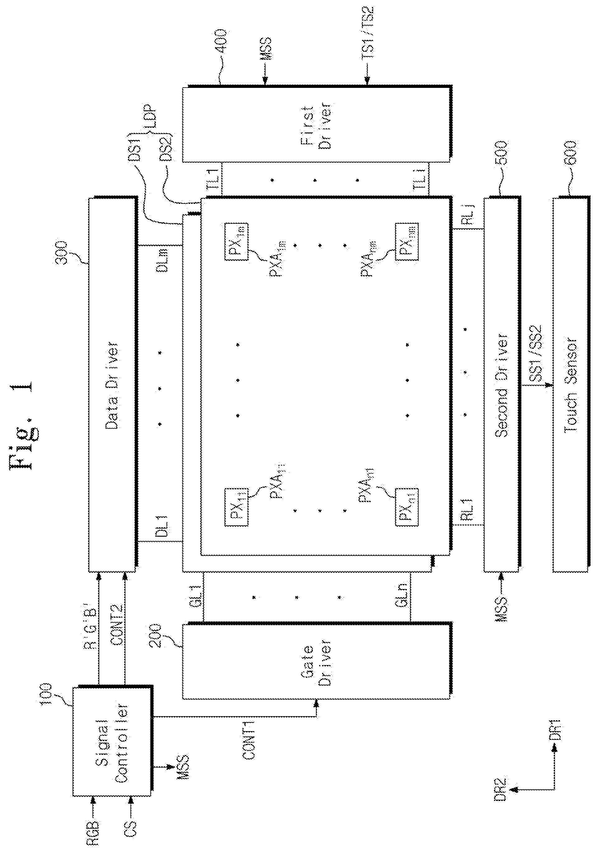
is a block diagram showing a display device according to exemplary embodiments of the present disclosure. is a perspective view showing a display panel shown in . is a plan view showing a display panel shown in . is a cross-sectional view taken along a line I-I′ shown in .
The display device includes a display panel LDP, a signal controller 100 , a gate driver 200 , a data driver 300 , and a touch panel. The touch panel includes a plurality of scan lines TL 1 to TLi (“i” is any whole number greater than 1), a plurality of source lines RL 1 to RLj (“j” is any whole number greater than 1), a first driver 400 , a second driver 500 , and a touch sensor 600 . The signal controller 100 , the gate driver 200 , and the data driver 300 control the display panel LDP to generate an image. The first driver 400 and the second driver 500 control the touch panel, and the touch sensor 600 calculates coordinate information of input positions.
Various display panels, such as a liquid crystal display panel, an organic light emitting display panel, an electrophoretic display panel, an electrowetting display panel, etc., may be used as the display panel LDP. According to exemplary embodiments of the present disclosure, in some cases, the display panel LDP may be a liquid crystal display panel, as described below.
A liquid crystal display (LCD) may also include a backlight unit (not shown) to supply a light to the liquid crystal display panel and a pair of polarizing plates (not shown). In addition, the liquid crystal display panel may include a vertical alignment mode panel, a patterned vertical alignment mode panel, an in-plane switching mode panel, a fringe-field switching mode panel, or a plane to line switching mode panel.
The display panel LDP includes a first display substrate DS 1 and a second display substrate DS 2 , which are disposed to be spaced apart from each other. One of the first display substrate DS 1 and the second display substrate DS 2 , which is disposed at a relatively upper position, provides an input device with an input surface.
The display panel LDP includes a plurality of gate lines GL 1 to GLn (“n” is any whole number greater than 1), a plurality of data lines DL 1 to DLm (“m” is any whole number greater than 1), and a plurality of pixels PX 11 to PXnm. Both of the gate lines GL 1 to GLn and the data lines DL 1 to DLm are disposed on either the first display substrate DS 1 or on the second display substrate DS 2 . In , the gate lines GL 1 to GLn and the data lines DL 1 to DLm are disposed on the first display substrate DS 1 .
The gate lines GL 1 to GLn are extended in a first direction DR 1 and arranged in a second direction DR 2 substantially perpendicular to the first direction DR 1 . The data lines DL 1 to DLm are extended in the second direction DR 2 and arranged in the first direction DR 1 . The data lines DL 1 to DLm are insulated from the gate lines GL 1 to GLn while crossing the gate lines GL 1 to GLn. The gate lines GL 1 to GLn are connected to the gate driver 200 , and the data lines DL 1 to DLm are connected to the data driver 300 .
The pixels PX 11 to PXnm are arranged in a matrix form. The pixels PX 11 to PXnm are arranged in pixel areas PXA 11 to PXAnm, respectively. Each of the pixels PX 11 to PXnm is connected to a corresponding gate line of the gate lines GL 1 to GLn and a corresponding data line of the data lines DL 1 to DLm.
The scan lines TL 1 to TLi and the source lines RL 1 to RLj are disposed on the substrate that provides the input surface. The scan lines TL 1 to TLi and the source lines RL 1 to RLj may be disposed on first display substrate DS 1 or the second display substrate DS 2 . shows nine scan lines TL 1 to TL 9 and ten source lines RL 1 to RL 10 , and shows a few scan lines TL of the scan lines TL 1 to TLj and one source line RL of the source lines RL 1 to RLj.
The scan lines TL 1 to TLi are disposed on a layer different from a layer on which the source lines RL 1 to RLj are disposed. The scan lines TL 1 to TLj are extended in the first direction DR 1 and arranged in the second direction DR 2 . The source lines RL 1 to RLj are extended in the second direction DR 2 and arranged in the first direction DR 1 . The scan lines TL 1 to TLi are connected to the first driver 400 and the source lines RL 1 to RLj are connected to the second driver 500 .
The scan lines TL 1 to TLi and the source lines RL 1 to RLj are formed of a transparent conductive material. In addition, the scan lines TL 1 to TLi and the source lines RL 1 to RLj may be formed of a metal material having a low reflectance.
The gate driver 200 and the data driver 300 may be disposed on the first display substrate DS 1 , and the first driver 400 and the second driver 500 may be disposed on the second display substrate DS 2 . The signal controller 100 and the touch sensor 600 are disposed on a circuit board connected to the display panel LDP.
Hereinafter, arrangements of the display panel LDP, the scan lines TL 1 to TL 9 , and the source lines RL 1 to RL 10 will be described in detail with reference to , 3 , and 4 .
The second display substrate DS 2 includes a plurality of transmitting areas TA and a blocking area SA. The blocking area SA surrounds the transmitting areas TA. The transmitting areas TA transmit light generated by and provided from the backlight unit and the blocking area SA blocks the light. The transmitting areas TA are arranged in a matrix form. The display device generates an image by combining the light transmitting through the transmitting areas TA.
Referring to , the scan lines TL 1 to TL 9 and the source lines RL 1 to RL 10 are disposed in the blocking area SA. Among the scan lines TL 1 to TL 9 , two scan lines adjacent to each other are disposed to be spaced apart from each other while interposing the transmitting areas TA arranged in the second direction DR 2 . Among the source lines RL 1 to RL 10 , two source lines adjacent to each other are disposed to be spaced apart from each other while interposing the transmitting areas TA arranged in the first direction DR 1 . The scan lines TL 1 to TL 9 and the source lines RL 1 to RL 10 are disposed to overlap with the blocking area SA. The scan lines TL 1 to TL 9 and the source lines RL 1 to RL 10 are not perceived to a user.
Referring to , the first display substrate DS 1 includes a first base substrate SUB 1 , a plurality of insulating layers 10 and 20 , and a plurality of conductive layers CE and PE. shows the plane to line switching mode panel, but the structure of the display panel should not be limited thereto or thereby.
Common electrodes CE are disposed on the first base substrate SUB 1 . A first insulating layer 10 is disposed on the first base substrate SUB 1 to cover the common electrodes CE. Pixel electrodes PE are disposed on the first insulating layer 10 . A second insulating layer 20 is disposed on the first insulating layer 10 to cover the pixel electrodes PE.
Each of the first and second insulating layers 10 and 20 is configured to include at least one organic layer and/or at least one inorganic layer. The gate lines GL 1 to GLn (refer to ) and the data lines DL 1 to DLm (refer to ) have not been shown in .
The pixel areas PXA are defined in the first display substrate DS 1 and the pixels PX are disposed on the first display substrate DS 1 . The pixel areas PXA are overlapped with the transmitting areas TA, respectively. As an example, shows three pixel areas PXA.
Each of the pixels PX includes a corresponding common electrode of the common electrodes CE and a corresponding pixel electrode of the pixel electrodes PE. In addition, each of the pixels PX further includes a thin film transistor connected to a corresponding data line of the data lines DL 1 to DLm, a corresponding gate line of the gate lines GL 1 to GLn, and a corresponding pixel electrode of the pixel electrodes PE.
The thin film transistor receives a pixel voltage from the pixel electrode PE. The common electrodes CE receive a common voltage. The common electrodes CE and the pixel electrodes PE form an electric field, and thus orientation arrangements of directors (e.g., liquid crystal molecules) included in the liquid crystal layer LCL are changed by the electric field. For example, in some cases, the common electrodes CE and the pixel electrodes PE form a horizontal electric field, and thus orientation arrangements of the liquid crystal molecules in the liquid crystal layer LCL are changed by the horizontal electric field.
As shown in , the second display substrate DS 2 includes a second base substrate SUB 2 , a black matrix BM, and a plurality of color filters CF. The black matrix BM includes a plurality of openings BM-OP formed therethrough. The scan lines TL and the source lines RL are disposed on the second base substrate SUB 2 . shows four scan lines TL and one source line RL. In , the one source line RL is presented to explain a layer structure of the second display substrate DS 2 . Practically, the one source line RL does not be overlapped with the plurality of openings BM-OP, and the one source line RL is overlapped with black matrix BM.
The black matrix BM is disposed on a lower surface of the second base substrate SUB 2 . The transmitting areas TA are defined by the openings BM-OP. In addition, the blocking area SA corresponds to an area in which the black matrix BM is disposed.
The color filters CF are disposed to overlap with the openings BM-OP, respectively. The color filters CF are respectively inserted into the openings BM-OP. The color filters CF include color filters having different colors from each other. For example, a portion of the color filters has a red color, another portion of the color filters has a green color, and the other portion of the color filters has a blue color.
The scan lines TL are disposed on the second base substrate SUB 2 . The scan lines TL may be directly disposed on the second base substrate SUB 2 . An insulating layer IL is disposed on the second base substrate SUB 2 to cover the scan lines TL. A protection layer PL is disposed on the insulating layer IL. The insulating layer IL may be, but not limited to, an adhesive layer. The protection layer PL may be an optical member, e.g., a polarizing plate.
The source line RL is disposed under the second base substrate SUB 2 . The source line RL is overlapped with the black matrix BM. The source line RL may be directly disposed on a lower surface of the second base substrate SUB 2 . In this case, the black matrix BM covers the source line RL. In some cases, the positions of the scan lines TL and the source line RL may be switched.
Referring to , the signal controller 100 receives input image signals RGB and converts the input image signals RGB to image data R′G′B′ corresponding to an operating mode of the display panel LDP. In addition, the signal controller 100 receives various control signals CS, such as a vertical synchronizing signal, a horizontal synchronizing signal, a main clock signal, a data enable signal, etc., and outputs first and second control signals CONT 1 and CONT 2 and a mode selection signal MSS.
The mode selection signal MSS determines the operating mode of the gate driver 200 and the touch panel. The touch panel may operate in an electrostatic capacitive mode (hereinafter, referred to as a first mode) or an electromagnetic induction mode (hereinafter, referred to as a second mode).
The mode selection signal MSS may be generated on the basis of the image displayed in the display panel LDP. The mode selection signal MSS may have different levels according to the operating modes. For instance, when the display panel LDP displays a keypad image, the mode selection signal MSS is output as a signal to activate the first mode, and when the display panel LDP displays a game image, the mode selection signal MSS is output as a signal to activate the second mode. In some cases, the mode selection signal MSS may be input by the user. For instance, the mode selection signal MSS is generated corresponding to an information inputted to a keypad by the user. The user may touch a first mode activating button.
The gate driver 200 applies gate signals to the gate lines GL 1 to GLn in response to the first control signal CONT 1 . The first control signal CONT 1 includes a vertical start signal to control and start an operation of the gate driver 200 , a gate clock signal to determine an output timing of a gate voltage, and an output enable signal that controls an ON-pulse width of the gate voltage.
The data driver 300 receives the second control signal CONT 2 and the image data R′G′B′. The data driver 300 converts the image data R′G′B′ to data voltages and applies the data voltages to the data lines DL 1 to DLm.
The second control signal CONT 2 includes a horizontal start signal to control and start an operation of the data driver 300 , an inverting signal to invert a polarity of the data voltages, and an output indicating signal that controls an output timing of the data voltages from the data driver 300 .
The first driver 400 receives the mode selection signal MSS. The first driver 400 receives first scan signals TS 1 and second scan signals TS 2 , and applies the first scan signals TS 1 or the second scan signals TS 2 to the scan lines TL 1 to TLi in response to the mode selection signal MSS. The first driver 400 outputs the first scan signals TS 1 in the first mode and outputs the second scan signals TS 2 in the second mode.
The second driver 500 receives the mode selection signal MSS. The second driver 500 outputs sensing signals SS 1 (hereinafter, referred to as first sensing signals) that represent a variation in capacitance of the source lines RL 1 to RLj during the first mode. The second driver 500 outputs sensing signals SS 2 (hereinafter, referred to as second sensing signals) according to a resonant frequency of the input device during the second mode. The input device may be, but is not limited to, a stylus pen with an inductor-capacitor (LC) resonant circuit.
The touch sensor 600 receives the first sensing signals SS 1 and the second sensing signals SS 2 . The touch sensor 600 calculates the coordinate information of an input position based on the first sensing signals SS 1 and the second sensing signals SS 2 . The input position in the first mode may be a position on the second display substrate DS 2 at which a touch of the input device is detected. In addition, the input position in the second mode may be a position on the second display substrate DS 2 at which a touch or an approach by the input device is detected.
is a block diagram showing a touch panel according to exemplary embodiments of the present disclosure. shows thirty-six scan lines TL 1 to TL 36 and thirty-six source lines RL 1 to RL 36 .
Referring to , the thirty-six scan lines TL 1 to TL 36 are grouped into four scan line groups TG 10 , TG 20 , TG 30 , and TG 40 (hereinafter, referred to first, second, third, and fourth scan line groups, respectively) and the thirty-six source lines RL 1 to RL 36 are grouped into four source line groups RG 10 , RG 20 , RG 30 , and RG 40 (hereinafter, referred to first, second, third, and fourth source line groups, respectively). Each of the first to fourth scan line groups TG 10 , TG 20 , TG 30 , and TG 40 includes a first scan line sub-group TLG 1 , a second scan line sub-group TLG 2 , and a third scan line sub-group TLG 3 . Each of the first scan line sub-group TLG 1 , the second scan line sub-group TLG 2 , and the third scan line sub-group TLG 3 includes at least one scan line.
The first scan line sub-group TLG 1 , the second scan line sub-group TLG 2 , and the third scan line sub-group TLG 3 include the same number of scan lines. For example, in , each scan line sub-group includes three scan lines. First ends of the three scan lines are connected to each other and the second ends of the three scan lines are connected to each other. It should be understood that various numbers of scan lines may be included in each scan line sub-group.
The first scan line sub-group TLG 1 , the second scan line sub-group TLG 2 , and the third scan line sub-group TLG 3 are arranged in the second direction DR 2 . The third scan line sub-group TLG 3 is disposed between the first scan line sub-group TLG 1 and the second scan line sub-group TLG 2 . The first scan line sub-group TLG 1 and the second scan line sub-group TLG 2 are connected to each other by a first connection line CNL 1 . Accordingly, the first scan line sub-group TLG 1 and the second scan line sub-group TLG 2 form one loop.
Each of the first to fourth source line groups RG 10 , RG 20 , RG 30 , and RG 40 includes a first source line sub-group RLG 1 , a second source line sub-group RLG 2 , and a third source line sub-group RLG 3 . Each of the first source line sub-group RLG 1 , the second source line sub-group RLG 2 , and the third source line sub-group RLG 3 includes at least one source line.
The first source line sub-group RLG 1 , the second source line sub-group RLG 2 , and the third source line sub-group RLG 3 include the same number of source lines. For example, in , each source line sub-group includes three source lines. First ends of the three source lines are connected to each other and second ends of the three source lines are connected to each other. It should be understood that various numbers of source lines may be included in each source line sub-group.
The first source line sub-group RLG 1 , the second source line sub-group RLG 2 , and the third source line sub-group RLG 3 are arranged in the first direction DR 1 . The third source line sub-group RLG 3 is disposed between the first source line sub-group RLG 1 and the second source line sub-group RLG 2 . The first source line sub-group RLG 1 and the second source line sub-group RLG 2 are connected to each other by a second connection line CNL 2 .
is a view showing the touch panel operated in the first mode. A and 7 B are views showing the touch panel operated in the second mode, and is a timing diagram showing signals generated in the second mode. Hereinafter, the operation of the touch panel will be described in detail with reference to , 7 A, 7 B, and 8 .
The touch panel operated in the first mode and shown in calculates the coordinate information of the input position in the same way as an electrostatic capacitive type touch panel. The first to fourth scan line groups TG 10 , TG 20 , TG 30 , and TG 40 correspond to input touch electrodes of the electrostatic capacitive type touch panel, and the first to fourth source line groups RG 10 , RG 20 , RG 30 , and RG 40 correspond to output touch electrodes of the electrostatic capacitive type touch panel.
The first to fourth scan line groups TG 10 , TG 20 , TG 30 , and TG 40 are capacitive-coupled to the first to fourth source line groups RG 10 , RG 20 , RG 30 , and RG 40 . Due to the capacitive coupling, capacitors are formed between the first to fourth scan line groups TG 10 , TG 20 , TG 30 , and TG 40 and the first to fourth source line groups RG 10 , RG 20 , RG 30 , and RG 40 .
The first to fourth scan line groups TG 10 , TG 20 , TG 30 , and TG 40 receive scan signals TS 1 - 1 to TS 1 - 4 (hereinafter, referred to as first scan signals), respectively, in different periods from each other. The first to fourth scan line groups TG 10 , TG 20 , TG 30 , and TG 40 sequentially receive the first scan signals TS 1 - 1 to TS 1 - 4 . The first to fourth source line groups RG 10 , RG 20 , RG 30 , and RG 40 output sensing signals SS 1 - 1 to SS 1 - 4 (hereinafter, referred to as first sensing signals), respectively.
An area in which the second scan line group TG 20 crosses the second source line group RG 20 may be the input position PP 1 (hereinafter, referred to as first input position). The first sensing signal SS 1 - 2 output from the second source line group RG 20 may then have a level different from a level of the first sensing signals SS 1 - 1 , SS 1 - 3 , and SS 1 - 4 of other source line groups RG 10 , RG 30 , and RG 40 .
The touch sensor 600 calculates a two-dimensional coordinate information of the first input position PP 1 based on a time at which the first sensing signal SS 1 - 2 having the different level is sensed and a relative position of the second source line group RG 20 with respect to the first to fourth source line groups RG 10 , RG 20 , RG 30 , and RG 40 .
The touch panel operated in the second mode (shown in A and 7 B ) calculates the coordinate information of the input position in the same way as an electromagnetic induction type touch panel. The first to fourth scan line groups TG 10 , TG 20 , TG 30 , and TG 40 correspond to input coils of the electromagnetic induction type touch panel, and the first to fourth source line groups RG 10 , RG 20 , RG 30 , and RG 40 correspond to output coils of the electromagnetic induction type touch panel.
Referring to A , the first to fourth scan line groups TG 10 , TG 20 , TG 30 , and TG 40 receive scan signals TS 2 - 1 to TS 2 - 4 (hereinafter, referred to as second scan signals), respectively, in different periods. The second scan signals TS 2 - 1 to TS 2 - 4 are respectively applied to the first ends of the first scan line sub-groups TLG 1 of the first to fourth scan line groups TG 10 , TG 20 , TG 30 , and TG 40 . The first end of the second scan line sub-group TLG 2 of each of the first to fourth scan line groups TG 10 , TG 20 , TG 30 , and TG 40 is grounded. The first end of the third scan line sub-group TLG 3 of each of the first to fourth scan line groups TG 10 , TG 20 , TG 30 , and TG 40 is floated without receiving any voltage.
Therefore, the first scan line sub-group TLG 1 and the second scan line sub-group TLG 2 form a current path. A magnetic field is induced by the current path formed by the first scan line sub-group TLG 1 and the second scan line sub-group TLG 2 . That is, the first scan line sub-group TLG 1 and the second scan line sub-group TLG 2 form one input coil. Since the first to fourth scan line groups TG 10 , TG 20 , TG 30 , and TG 40 receive the second scan signals TS 2 - 1 to TS 2 - 4 in different periods, the magnetic field is induced in different periods.
When the input device (not shown) approaches the first to fourth scan line groups TG 10 , TG 20 , TG 30 , and TG 40 , the magnetic field induced from the first to fourth scan line groups TG 10 , TG 20 , TG 30 , and TG 40 resonates with the resonant circuit of the input device. Thus, the input device generates the resonant frequency.
Referring to B , the first to fourth source line groups RG 10 , RG 20 , RG 30 , and RG 40 output sensing signals SS 2 - 1 to SS 2 - 4 (hereinafter, referred to as second sensing signals), respectively, according to the resonant frequency of the input device. The second sensing signals SS 2 - 1 to SS 2 - 4 are output from the first ends of the first source line sub-groups RGL 1 of the first to fourth source line groups RG 10 , RG 20 , RG 30 , and RG 40 . The first end of the second source line sub-group RLG 2 of each of the first to fourth source line groups RG 10 , RG 20 , RG 30 , and RG 40 is grounded. The first end of the third source line sub-group RLG 3 of each of the first to fourth source line groups RG 10 , RG 20 , RG 30 , and RG 40 is floated without receiving any voltage.
An input position PP 2 (hereinafter, referred to as second input position) may correspond to an area in which the second scan line group TG 20 crosses the second source line group RG 20 . The second sensing signal SS 2 - 2 output from the second source line group RG 20 has a level different from a level of the second sensing signals SS 2 - 1 , SS 2 - 3 , and SS 2 - 4 of other source line groups RG 10 , RG 30 , and RG 40 .
The touch sensor 600 calculates a two-dimensional coordinate information of the second input position PP 2 based on a time at which the second sensing signal SS 2 - 2 having the different level is sensed and a relative position of the second source line group RG 20 with respect to the first to fourth source line groups RG 10 , RG 20 , RG 30 , and RG 40 .
Referring to A, 7 B, and 8 , the second scan signals TS 2 - 1 to TS 2 - 4 are sequentially applied to the first scan line sub-groups TLG 1 of the first to fourth scan line groups TG 10 , TG 20 , TG 30 , and TG 40 . An induction signal RS is generated from the input device disposed at the second input position PP 2 .
After the second scan signal TS 2 - 2 applied to the second scan line group TG 20 is deactivated, the induction signal RS is gradually decreased during a predetermined period. The input device generates a frequency corresponding to the induction signal RS that is gradually decreased. The frequency generated by the input device generates the second sensing signal SS 2 - 2 of the second source line group RG 20 .
is a block diagram showing the first driver 400 shown in . is a circuit diagram showing switching parts 430 - 1 to 430 - 4 shown in . Hereinafter, the first driver 400 will be described in detail with reference to .
The first driver 400 includes a scan signal output part 410 , a selection part 420 , and switching parts 430 - 1 to 430 - 4 . shows four switching parts 430 - 1 to 430 - 4 (hereinafter, referred to as first to fourth switching parts, respectively).
The scan signal output part 410 receives the mode selection signal MSS, the first scan signal TS 1 , and the second scan signal TS 2 . The first and second scan signals TS 1 and TS 2 may be provided from an external circuit, e.g., a scan signal generating circuit. The scan signal output part 410 selectively outputs the first scan signal TS 1 and the second scan signal TS 2 in response to the mode selection signal MSS.
The selection part 420 switches the first to fourth switching parts 430 - 1 to 430 - 4 . The selection part 420 receives the mode selection signal MSS and outputs switching control signals SW- 1 to SW- 4 and SW- 10 to SW- 40 having different turn-on periods. The selection part 420 outputs first switching control signals SW- 1 to SW- 4 in the first mode and outputs second switching control signals SW- 10 to SW- 40 in the second mode. The second switching control signals SW- 10 to SW- 40 have phases opposite to those of the first switching control signals SW- 1 to SW- 4 .
Each of the first to fourth switching parts 430 - 1 to 430 - 4 receives the first scan signal TS 1 from the scan signal output part 410 in the first mode and receives the second scan signal TS 2 from the scan signal output part 410 in the second mode. The first to fourth switching parts 430 - 1 to 430 - 4 respectively receive the first switching control signals SW- 1 to SW- 4 in the first mode and respectively receive the second switching control signals SW- 10 to SW- 40 in the second mode.
In the first mode, the first to fourth switching parts 430 - 1 to 430 - 4 apply the first scan signal TS 1 to the first to fourth scan line groups TG 10 , TG 20 , TG 30 , and TG 40 in response to the first switching control signals SW- 1 to SW- 4 . In the second mode, the first to fourth switching parts 430 - 1 to 430 - 4 apply the second scan signal TS 2 to the first to fourth scan line groups TG 10 , TG 20 , TG 30 , and TG 40 in response to the second switching control signals SW- 10 to SW- 40 .
Referring to , each of the first to fourth switching parts 430 - 1 to 430 - 4 includes a first switch ST 1 , a second switch ST 2 , and a third switch ST 3 . Hereafter, the first switch 430 - 1 will be described as a representative example.
The first switch ST 1 applies the first scan signal TS 1 to the first scan line sub-group TLG 1 in the first mode and applies the second scan signal TS 2 to the first scan line sub-group TLG 1 in the second mode.
The first switch ST 1 may be, but is not limited to, a Complementary Metal-Oxide Semiconductor (CMOS) transistor. The CMOS transistor includes an n-type transistor and a p-type transistor. Control electrodes of the n-type transistor and the p-type transistor are commonly connected to each other to receive the first switching control signal SW- 1 and the second switching control signal SW- 10 . In some cases, the first switching control signal SW- 1 has a high level in the turn-on period and the second switching control signal SW- 10 has a low level in the turn-on period.
An input electrode of the n-type transistor receives the first scan signal TS 1 and an input electrode of the p-type transistor receives the second scan signal TS 2 . An output electrode of the n-type transistor and an output electrode of the p-type transistor are commonly connected to the first scan line sub-group TLG 1 .
The second switch ST 2 applies the first scan signal TS 1 to the second scan line sub-group TLG 2 in the first mode and applies the second scan signal TS 2 to the second scan line sub-group TLG 2 in the second mode.
The second switch ST 2 may be, but is not limited to, a CMOS transistor. Control electrodes of an n-type transistor and a p-type transistor of the second switch ST 2 are commonly connected to each other to receive the first switching control signal SW- 1 and the second switching control signal SW- 10 .
An input electrode of the n-type transistor receives the first scan signal TS 1 and an input electrode of the p-type transistor receives a ground voltage. An output electrode of the n-type transistor and an output electrode of the p-type transistor are commonly connected to the second scan line sub-group TLG 2 .
The n-type transistor of each of the first and second switches ST 1 and ST 2 , which are turned on in the first mode, applies the first scan signal TS 1 to the first and second scan line sub-groups TLG 1 and TLG 2 . The p-type transistor of each of the first and second switches ST 1 and ST 2 , which are turned on in the second mode, forms a current path in the first scan signal TS 1 to the first and second scan line sub-groups TLG 1 and TLG 2 .
The third switch ST 3 applies the first scan signal TS 1 to the third scan line sub-group TLG 3 in the first mode and floats the third scan line sub-group TLG 3 in the second mode.
The third switch ST 3 may be, but is not limited to, an n-channel MOS (NMOS) transistor. A control electrode of the NMOS transistor receives the first switching control signal SW- 1 and the second switching control signal SW- 10 . An input electrode of the NMOS transistor receives the first scan signal TS 1 and an output electrode of the NMOS transistor is connected to the third scan line sub-group TLG 3 . In the second mode, the third switch ST 3 is turned off by the second switching control signal SW- 10 having the low level, and thus the third scan line sub-group TLG 3 is floated.
In some cases, the n-type transistor and the p-type transistor of the CMOS transistor may be switched. In such cases, the third switch ST 3 may be a p-channel MOS (PMOS) transistor.
is a block diagram showing the second driver 500 and the touch sensor shown 600 in , and is a circuit diagram showing a sensing signal output part shown in . Hereinafter, the second driver 500 and the touch sensor 600 will be described in detail with reference to .
Referring to , the second driver 500 includes a plurality of sensing signal output parts 502 , 504 , 506 , and 508 . shows four sensing signal output parts 502 , 504 , 506 , and 508 (hereinafter, referred to as first to fourth sensing signal output parts, respectively).
The first to fourth sensing signal output parts 502 , 504 , 506 , and 508 are connected to the first to fourth source line groups RG 10 , RG 20 , RG 30 , and RG 40 , respectively. Each of the first to fourth sensing signal output parts 502 , 504 , 506 , and 508 receives a control signal. The control signal may be the mode selection signal MSS. In some cases, the control signal may be another signal having the same phase as the mode selection signal MSS.
In the first mode, the first to fourth sensing signal output parts 502 , 504 , 506 , and 508 output the first sensing signals SS 1 - 1 to SS 1 - 4 (refer to ) from the first to fourth source line groups RG 10 , RG 20 , RG 30 , and RG 40 . In the second mode, the first to fourth sensing signal output parts 502 , 504 , 506 , and 508 output the second sensing signals SS 2 - 1 to SS 2 - 4 (refer to B ) from the first to fourth source line groups RG 10 , RG 20 , RG 30 , and RG 40 .
Referring to , each of the first to fourth sensing signal output parts 502 , 504 , 506 , and 508 includes a first switch ST 10 , a second switch ST 20 , and a third switch ST 30 . Hereinafter, the first sensing signal output part 502 will be described as a representative example.
The first switch ST 10 outputs the first sensing signal SS 1 - 1 from the first end of the first source line sub-group RLG 1 in the first mode and outputs the second sensing signal SS 2 - 1 from the first end of the first source line sub-group RLG 1 in the second mode. The first switch ST 10 may be, but is not limited to, a CMOS transistor.
The CMOS transistor includes an n-type transistor and a p-type transistor. Control electrodes of the n-type transistor and the p-type transistor are commonly connected to each other to receive the mode selection signal MSS. The mode selection signal MSS has a high level in the first mode and a low level in the second mode.
An input electrode of the n-type transistor is connected to the first source line sub-group RLG 1 and an output electrode of the n-type transistor is connected to the touch sensor 600 . An input electrode of the p-type transistor is connected to the first source line sub-group RLG 1 and an output electrode of the p-type transistor is connected to the touch sensor 600 . The output electrode of the n-type transistor applies the first sensing signal SS 1 - 1 to the touch sensor 600 and the output electrode of the p-type transistor applies the second sensing signal SS 2 - 1 to the touch sensor 600 .
The second switch ST 20 outputs the first sensing signal SS 1 - 1 from the first end of the second source line sub-group RLG 2 in the first mode and grounds the second source line sub-group RLG 2 in the second mode. The second switch ST 20 may be, but is not limited to, a CMOS transistor.
Control electrodes of the n-type transistor and the p-type transistor of the second switch ST 20 are commonly connected to each other to receive the mode selection signal MSS. An input electrode of the n-type transistor is connected to the second source line sub-group RLG 2 and an output electrode of the n-type transistor is connected to the touch sensor 600 . An input electrode of the p-type transistor is connected to the second source line sub-group RLG 2 and an output electrode of the p-type transistor receives the ground voltage.
The third switch ST 30 outputs the first sensing signal SS 1 - 1 to the touch sensor 600 in the first mode and floats the third source line sub-group RLG 3 in the second mode.
The third switch ST 30 may be, but is not limited to, an NMOS transistor. A control electrode of the NMOS transistor receives the mode selection signal MSS. An input electrode of the NMOS transistor is connected to the third source line sub-group RLG 3 and an output electrode of the NMOS transistor is connected to the touch sensor 600 . In some cases, the n-type transistor and the p-type transistor of the CMOS may be switched. In such cases, the third switch ST 30 may be a PMOS transistor.
Referring to again, the touch sensor 600 includes signal processors 610 - 1 to 610 - 4 (hereinafter, referred to as first to fourth signal processing parts, respectively), a multiplexer 620 , and a coordinate calculator 630 .
The first to fourth signal processors 610 - 1 to 610 - 4 respectively receive the first sensing signals SS 1 - 1 to SS 1 - 4 (refer to ) from the first to fourth sensing signal output parts 502 , 504 , 506 , and 508 in the first mode and respectively receive the second sensing signals SS 2 - 1 to SS 2 - 4 (refer to B ) from the first to fourth sensing signal output parts 502 , 504 , 506 , and 508 in the second mode. Each of the first to fourth signal processors 610 - 1 to 610 - 4 includes a first mode signal processor (not shown) to process the first sensing signals SS 1 - 1 to SS 1 - 4 and a second mode signal processor (not shown) to process the second sensing signals SS 2 - 1 to SS 2 - 4 .
The first mode signal processor includes an amplifier, a noise filter, and an analog-to-digital converter. The amplifier amplifies the first sensing signals SS 1 - 1 to SS 1 - 4 . The noise filter removes noises from the amplified first sensing signals SS 1 - 1 to SS 1 - 4 . The analog-to-digital converter converts the first sensing signals SS 1 - 1 to SS 1 - 4 from which the noises are removed to first digital signals.
The second mode signal processor includes an amplifier, a band-pass filter, a wave detector, a sample-hold circuit, and an analog-to-digital converter. The second sensing signals SS 2 - 1 to SS 2 - 4 are converted to second digital signals using the second mode signal processor.
The multiplexer 620 selectively applies the first and second digital signals from the first to fourth signal processors 610 - 1 to 610 - 4 to the coordinate calculator 630 . The coordinate calculator 630 compares the first and second digital signals to a reference value to sense the output touch electrode or the output coil in which the external input occurs. The coordinate calculator 630 calculates the coordinate information of the first input position PP 1 (refer to ) from the first digital signals and calculates the coordinate information of the second input position PP 2 (refer to B ) from the second digital signals.
are cross-sectional views showing display panels according to exemplary embodiments of the present disclosure. In , the same reference numerals denote the same elements in to 3 , and thus detailed descriptions of the same elements will be omitted.
Referring to , the scan lines TL and the source lines RL are disposed on or under the second base substrate SUB 2 . In , the scan lines TL and the source lines RL are disposed under the second base substrate SUB 2 . In , the scan lines TL and the source lines RL are disposed on the second base substrate SUB 2 .
Referring to , a black matrix BM including a plurality of openings BM-OP is disposed on a lower surface of the second base substrate SUB 2 of the display panel LDP 10 . Color filters CF are disposed in the openings BM-OP. The scan lines TL and the source lines RL are disposed to overlap, at least partially, with the black matrix BM.
The scan lines TL are disposed on a lower surface of the black matrix BM. A third insulating layer IL- 1 is disposed on the black matrix BM and the color filters CF to cover the scan lines TL. The third insulating layer IL- 1 provides a flat surface thereon. A fourth insulating layer IL- 2 is disposed on the third insulating layer IL- 1 to cover the source lines RL. Each of the third insulating layer IL- 1 and the fourth insulating layer IL- 2 includes at least one organic layer and/or at least one inorganic layer.
Referring to , a black matrix BM including a plurality of openings BM-OP is disposed on a lower surface of the second base substrate SUB 2 of the display panel LDP 20 . Color filters CF are disposed in the openings BM-OP. The source lines RL are disposed on an upper surface of the second base substrate SUB 2 to overlap, at least partially, with the black matrix BM.
A third insulating layer IL- 1 is disposed on the upper surface of the second base substrate SUB to cover the source lines RL. The third insulating layer IL- 1 provides a flat surface thereon. The scan lines TL are disposed on the third insulating layer IL- 1 . A fourth insulating layer IL- 2 is disposed on the third insulating layer IL- 1 to cover the scan lines TL. A protection layer PL is disposed on the fourth insulating layer IL- 2 . In some cases, the positions of the scan lines TL and the source lines RL may be switched.
A and 15 B are plan views showing display panels according to exemplary embodiments of the present disclosure. In A and 15 B , the same reference numerals denote the same elements in to 3 , and thus detailed descriptions of the same elements will be omitted.
Referring to A and 15 B , a plurality of scan lines TL 1 to TL 9 and a plurality of source lines RL 1 to RL 10 are disposed in the blocking area SA. Each of the scan lines TL 1 to TL 9 further includes first sensing electrodes SSE 1 disposed at positions in which each of the scan lines TL 1 to TL 9 crosses the source lines RL 1 to RL 10 . In addition, each of the source lines RL 1 to RL 9 further includes second sensing electrodes SSE 2 disposed at positions in which each of the source lines RL 1 to RL 9 crosses the scan lines TL 1 to TL 9 .
The first sensing electrodes SSE 1 are overlapped with the second sensing electrodes SSE 2 . The overlap areas between the scan lines TL 1 to TL 9 and the source lines RL 1 to RL 10 are increased by the first sensing electrodes SSE 1 and the second sensing electrodes SSE 2 . Accordingly, the capacitance variation of capacitors formed between the scan lines TL 1 to TL 9 and the source lines RL 1 to RL 10 becomes large. Therefore, touch sensitivity in the first mode may be improved. In some cases, either the first sensing electrodes SSE 1 or the second sensing electrodes SSE 2 may be omitted.
is a block diagram showing a touch panel according to exemplary embodiments of the present disclosure, is a view showing a touch panel operated in a first mode. A and 18 B are views showing touch panels operated in a second mode. In , 17 , 18 A, and 18 B , the same reference numerals denote the same elements in to 15 B , and thus detailed descriptions of the same elements will be omitted.
With respect to , a display device includes a display panel LDP (refer to ), a signal controller 100 (refer to ), a gate driver 200 (refer to ), a data driver 300 (refer to ), first drivers 400 - 1 and 400 - 2 , second drivers 500 - 1 and 500 - 2 , and a touch sensor 600 . to 18 B show thirty-six scan lines TL 1 to TL 36 and thirty-six source lines RL 1 to RL 36 . The first and second scan drivers 400 - 1 and 400 - 2 , the first and second source drivers 500 - 1 and 500 - 2 , the touch sensor 600 , the scan lines TL 1 to TL 36 , and the source lines RL 1 to RL 36 form the touch panel.
Referring to to 18 B , the scan lines TL 1 to TL 36 are extended in the first direction DR 1 and arranged in the second direction DR 2 . The source lines RL 1 to RL 36 are extended in the second direction DR 2 and arranged in the first direction DR 1 . The scan lines TL 1 to TL 36 are grouped into four scan line groups TG 10 , TG 20 , TG 30 , and TG 40 , and the source lines RL 1 to RL 36 are grouped into four source line groups RG 10 , RG 20 , RG 30 , and RG 40 .
Each of the first to fourth scan line groups TG 10 , TG 20 , TG 30 , and TG 40 includes a first scan line sub-group TLG 1 , a second scan line sub-group TLG 2 , and a third scan line sub-group TLG 3 . The third scan line sub-group TLG 3 is disposed between the first scan line sub-group TLG 1 and the second scan line sub-group TLG 2 . Each of the first scan line sub-group TLG 1 , the second scan line sub-group TLG 2 , and the third scan line sub-group TLG 3 includes at least one scan line.
The first scan line sub-group TLG 1 , the second scan line sub-group TLG 2 , and the third scan line sub-group TLG 3 include the same number of scan lines. For instance, each scan line sub-group includes three scan lines as shown in . It should be understood that various numbers of scan lines may be included in each scan line sub-group. The three scan lines are connected to each other at two ends thereof.
Each of the first to fourth source line groups RG 10 , RG 20 , RG 30 , and RG 40 includes a first source line sub-group RLG 1 , a second source line sub-group RLG 2 , and a third source line sub-group RLG 3 . The third source line sub-group RLG 3 is disposed between the first source line sub-group RLG 1 and the second source line sub-group RLG 2 . Each of the first source line sub-group RLG 1 , the second source line sub-group RLG 2 , and the third source line sub-group RLG 3 includes at least one source line.
The first source line sub-group RLG 1 , the second source line sub-group RLG 2 , and the third source line sub-group RLG 3 include the same number of source lines. Three source lines of each of the first to third source line sub-groups RLG 1 to RLG 3 are connected to each other at two ends thereof. It should be understood that various numbers of source lines may be included in each source line sub-group.
The first scan driver 400 - 1 is connected to first ends of the first to fourth scan line groups TG 10 , TG 20 , TG 30 , and TG 40 , and the second scan driver 400 - 2 is connected to the second ends of the first to fourth scan line groups TG 10 , TG 20 , TG 30 , and TG 40 . For instance, the first scan driver 400 - 1 is connected to the first end of the first scan line sub-group TLG 1 , the second scan line sub-group TLG 2 , and the third scan line sub-group TLG 3 of each of the first to fourth scan line groups TG 10 , TG 20 , TG 30 , and TG 40 . The second scan driver 400 - 2 is connected to the second end of the first scan line sub-group TLG 1 and the second scan line sub-group TLG 2 of each of the first to fourth scan line groups TG 10 , TG 20 , TG 30 , and TG 40 .
The first source driver 500 - 1 is connected to first ends of the first to fourth source line groups RG 10 , RG 20 , RG 30 , and RG 40 , and the second source driver 500 - 2 is connected to the second ends of the first to fourth source line groups RG 10 , RG 20 , RG 30 , and RG 40 . For example, the first source driver 500 - 1 is connected to the first end of the first source line sub-group RLG 1 , the second source line sub-group RLG 2 , and the third source line sub-group RLG 3 of each of the first to fourth source line groups RG 10 , RG 20 , RG 30 , and RG 40 . The second source driver 500 - 2 is connected to the second end of the first source line sub-group RLG 1 and the second source line sub-group RLG 2 of each of the first to fourth source line groups RG 10 , RG 20 , RG 30 , and RG 40 .
shows the touch panel operated in the first mode. The touch panel operated in the first mode calculates the coordinate information of the input position in the same way as an electrostatic capacitive type touch panel. The method of calculating the coordinate information of the input position is the same as that described with reference to , and thus detailed descriptions thereof will be omitted.
The touch panel shown in A and 18 B and operated in the second mode calculates the coordinate information of the input position in the same way as an electromagnetic induction type touch panel. The first to fourth scan line groups TG 10 , TG 20 , TG 30 , and TG 40 correspond to input coils of the electromagnetic induction type touch panel, and the first to fourth source line groups RG 10 , RG 20 , RG 30 , and RG 40 correspond to output coils of the electromagnetic induction type touch panel.
Referring to A , the first to fourth scan line groups TG 10 , TG 20 , TG 30 , and TG 40 receive second scan signals TS 2 - 1 to TS 2 - 4 in different periods. The second scan signals TS 2 - 1 to TS 2 - 4 are respectively applied to first ends of the first scan line sub-groups TLG 1 and to second ends of the second scan line sub-group TLG 2 of the first to fourth scan line groups TG 10 , TG 20 , TG 30 , and TG 40 . The second end of the first scan ling sub-group TLG 1 and the first end of the second scan line sub-group TLG 2 of each of the first to fourth scan line groups TG 10 , TG 20 , TG 30 , and TG 40 are grounded. The third scan line sub-group TLG 3 of each of the first to fourth scan line groups TG 10 , TG 20 , TG 30 , and TG 40 is floated without receiving any voltage.
In the second mode, a direction in which a current flows through the first scan line sub-group TLG 1 of each of the first to fourth scan line groups TG 10 , TG 20 , TG 30 , and TG 40 is opposite to a direction in which a current flows through the second scan line sub-group TLG 2 of each of the first to fourth scan line groups TG 10 , TG 20 , TG 30 , and TG 40 . A magnetic field is induced by the currents flowing through the first scan line sub-group TLG 1 and the second scan line sub-group TLG 2 in opposite directions. Although the first scan line sub-group TLG 1 is not connected to the second scan line sub-group TLG 2 , the first scan line sub-group TLG 1 and the second scan line sub-group TLG 2 form one coil. Since the first to fourth scan line groups TG 10 , TG 20 , TG 30 , and TG 40 receive the second scan signals TS 2 - 1 to TS 2 - 4 in different periods, the magnetic field is induced in different periods.
When the input device (not shown) approaches the first to fourth scan line groups TG 10 , TG 20 , TG 30 , and TG 40 , the magnetic field induced from the first to fourth scan line groups TG 10 , TG 20 , TG 30 , and TG 40 resonates with the resonant circuit of the input device. Thus, the input device causes generation of the resonant frequency.
Referring to B , the first to fourth source line groups RG 10 , RG 20 , RG 30 , and RG 40 output second sensing signals SS 2 - 1 to SS 2 - 4 according to the resonant frequency of the input device. The second sensing signals SS 2 - 1 to SS 2 - 4 are output from the first ends of the first source line sub-groups RGL 1 and the second ends of the second source line sub-groups RLG 2 of the first to fourth source line groups RG 10 , RG 20 , RG 30 , and RG 40 . The second end of the first source line sub-group RLG 1 and the first end of the second source line sub-group RLG 2 of each of the first to fourth source line groups RG 10 , RG 20 , RG 30 , and RG 40 are grounded. The third source line sub-group RLG 3 of each of the first to fourth source line groups RG 10 , RG 20 , RG 30 , and RG 40 is floated without receiving any voltage.
The touch sensor 600 calculates the coordinate information about the input position based on the second sensing signals SS 2 - 1 to SS 2 - 4 provided from at least one of the first end of the first source line sub-group RLG 1 of each of the first to fourth source line groups RG 10 , RG 20 , RG 30 , and RG 40 or the second end of the second source line sub-group RLG 2 of each of the first to fourth source line groups RG 10 , RG 20 , RG 30 , and RG 40 .
is a bock diagram showing the second scan driver 400 - 2 according to exemplary embodiments of the present disclosure. is a block diagram showing the second source driver 500 - 2 according to exemplary embodiments of the present disclosure. Hereinafter, the second scan driver 400 - 2 and the second source driver 500 - 2 will be described in detail with reference to . The first scan driver 400 - 1 may have the same or similar configuration and function as the configuration and function of the first driver 400 described with reference to , and thus the detailed description of the first scan driver 400 - 1 will be omitted. In addition, the first source driver 500 - 1 may have the same configuration and function as the configuration and function of the second driver 500 described with reference to , and thus the detailed description of the first source driver 500 - 1 will be omitted.
Referring to , the second scan driver 400 - 2 includes switching parts 440 - 1 to 440 - 4 . The switching parts 440 - 1 to 440 - 4 respectively receive the first switching control signals SW- 1 to SW- 4 in the first mode and respectively receive the second switching control signals SW- 10 to SW- 40 in the second mode.
The switching parts 440 - 1 to 440 - 4 float the second end of the first scan line sub-group TLG 1 and the second end of the second scan line sub-group TLG 2 of each of the first to fourth scan line groups TG 10 , TG 20 , TG 30 , and TG 40 in the first mode. The switching parts 440 - 1 to 440 - 4 ground the second end of the first scan line sub-group TLG 1 of each of the first to fourth scan line groups TG 10 , TG 20 , TG 30 , and TG 40 in the second mode and apply the second scan signals TS 2 - 1 to TS 2 - 4 to the second end of the second scan line sub-group TLG 2 of each of the first to fourth scan line groups TG 10 , TG 20 , TG 30 , and TG 40 in the second mode.
Among the switching parts 440 - 1 to 440 - 4 , two switching parts 440 - 1 and 440 - 4 have been shown in as an example. Each of the switching parts 440 - 1 to 440 - 4 includes a first switch ST 100 and a second switch ST 200 .
The first switch ST 100 is turned off in the first mode and turned on in the second mode to apply the ground voltage to the second end of the first scan line sub-group TLG 1 . The second switch ST 200 is turned off in the first mode and turned on in the second mode to apply the second scan signal TS 2 - 1 to the second end of the second scan line sub-group TLG 2 . The first switch ST 100 and the second switch ST 200 may be a PMOS transistor or a NMOS transistor. shows PMOS transistors as a representative example.
Referring to , the second source driver 500 - 2 includes a plurality of switching parts 512 to 518 . shows four switching parts 512 to 518 as an example. Each of the switching parts 512 to 518 receives the mode selection signal MSS.
The switching parts 512 to 518 float the second end of the first source line sub-group RLG 1 and the second end of the second source line sub-group RLG 2 of each of the first to fourth source line groups RG 10 , RG 20 , RG 30 , and RG 40 in the first mode. The switching parts 512 to 518 ground the second end of the first source line sub-group RLG 1 of each of the first to fourth source line groups RG 10 , RG 20 , RG 30 , and RG 40 in the second mode and output the second sensing signal SS 2 - 1 from the second end of the second source line sub-group RLG 2 . The second sensing signal SS 2 - 1 output from the second end of the second source line sub-group RLG 2 may be applied to the touch sensor 600 .
Among the switching parts 512 to 518 , two switching parts 512 and 518 have been shown in as an example. Each of the switching parts 512 to 518 includes a first switch ST 1000 and a second switch ST 2000 . Responsive to the mode selection signal MSS, the first and second switches ST 1000 and ST 2000 are turned off in the first mode and turned on in the second mode. The first switch ST 1000 and the second switch ST 2000 may be a PMOS transistor or a NMOS transistor. shows PMOS transistors as a representative example.
is a block diagram showing a display device according to exemplary embodiments of the present disclosure. is a partial perspective view showing a display panel and a touch panel shown in . A and 23 B are cross-sectional views taken along a line I-I′ shown in . shows the display panel DP and the touch panel TP, which are dislocated from each other to separately show the display panel DP and the touch panel TP.
Referring to , the display device includes a display panel DP, a signal controller 100 , a gate driver 200 , a data driver 300 , and a touch panel TP. The signal controller 100 , the gate driver 200 , and the data driver 300 control the display panel DP to generate an image. Although not shown in figures, the display device further includes a touch panel driver to drive the touch panel TP and a touch sensor to calculate coordinate information of an input position.
The display panel DP may be various types of display panels, including, for example a LCD panel. The display panel DP includes a plurality of gate lines GL 1 to GLn, a plurality of data lines DL 1 to DLm, and a plurality of pixels PX 11 to PXnm. The gate lines GL 1 to GLn are extended in a first direction DR 1 and arranged in a second direction DR 2 substantially perpendicular to the first direction DR 1 . The data line DL 1 to DLm are extended in the second direction DR 2 and arranged in the first direction DR 1 . The data lines DL 1 to DLm are insulated from the gate lines GL 1 to GLn while crossing the gate lines GL 1 to GLn.
The pixels PX 11 to PXnm are arranged in a matrix form. The pixels PX 11 to PXnm are arranged in pixel areas PXA 11 to PXAnm, respectively. Each of the pixels PX 11 to PXnm is connected to a corresponding gate line of the gate lines GL 1 to GLn and a corresponding data line of the data lines DL 1 to DLm.
The signal controller 100 receives input image signals RGB and converts the input image signals RGB to image data R′G′B′ corresponding to an operating mode of the display panel DP. In addition, the signal controller 100 receives various control signals CS, such as a vertical synchronizing signal, a horizontal synchronizing signal, a main clock signal, a data enable signal, etc., and outputs first and second control signals CONT 1 and CONT 2 and a mode selection signal MSS.
The mode selection signal MSS determines the operating mode of the touch panel TP. The touch panel TP is operated in an electrostatic capacitive mode (hereinafter, referred to as a first mode), an electromagnetic induction mode (hereinafter, referred to as a second mode), or a hybrid mode (hereinafter, referred to as a third mode).
The mode selection signal MSS may be generated on the basis of the image displayed in the display panel DP. The mode selection signal MSS may have different levels corresponding to the operating modes. For instance, when the display panel DP displays a keypad image, the mode selection signal MSS is output as a signal to activate the first mode, and when the display panel DP displays a background image, the mode selection signal MSS is output as a signal to activate the third mode. In some cases, the mode selection signal MSS may be input by the user. For instance, the mode selection signal MSS is generated corresponding to an information inputted to a keypad by the user. The user may touch a first mode activating button.
The gate driver 200 applies gate signals to the gate lines GL 1 to GLn in response to the first control signal CONT 1 . The data driver 300 receives the second control signal CONT 2 and the image data R′G′B′. The data driver 300 converts the image data R′G′B′ to data voltages and applies the data voltages to the data lines DL 1 to DLm.
Referring to , the display panel DP includes a first display substrate DS 1 and a second display substrate DS 2 , which are disposed to be spaced apart from each other. A liquid crystal layer LCL is disposed between the first display substrate DS 1 and the second display substrate DS 2 . The gate lines GL 1 to GLn (refer to ), the data lines DL 1 to DLm (refer to ), and the pixels PX 11 to PXnm (refer to ) may be disposed on the first display substrate DS 1 or the second display substrate DS 1 .
Hereinafter, to explain the exemplary embodiments, the gate lines GL 1 to GLn, the data lines DL 1 to DLm, and the pixels PX 11 to PXnm are assumed to be disposed on the first display substrate DS 1 . The second display substrate DS 2 includes a plurality of transmitting areas TA and a blocking area SA. The blocking area SA surrounds the transmitting areas TA. The transmitting areas TA transmit light generated by and provided from the backlight unit, and the blocking area SA blocks the light.
The touch panel TP is disposed on the display panel DP. The touch panel TP may be attached to the upper surface of the second display substrate DS 2 . The touch panel TP includes a first touch substrate TSS 1 , a first conductive layer CL 1 , an insulating layer IL, a second conductive layer CL 2 , and a second touch substrate TSS 2 .
The first touch substrate TSS 1 and the second touch substrate TSS 2 may be configured to include a plastic substrate, a glass substrate, or a film. In addition, the first touch substrate TSS 1 and the second touch substrate TSS 2 may be an optical film, e.g., a polarizing plate. The first conductive layer CL 1 and the second conductive layer CL 2 may be configured to include a transparent metal oxide material or a metal material with a low reflectivity including at least one of chromium oxide, chromium nitride, titanium oxide, titanium nitride, or alloys thereof. The insulating layer IL may be configured to include an organic insulating material or an inorganic insulating material.
Although not shown in , each of the first and second conductive layers CL 1 and CL 2 includes a plurality of conductive patterns. The conductive patterns of the first conductive layer CL 1 are configured to include portions (e.g., first portions) of first touch electrodes, second touch electrodes, first touch coils, and second touch coils, and the conductive patterns of the second conductive layer CL 2 are configured to include other portions (e.g., second portions) of first touch electrodes, second touch electrodes, first touch coils, and second touch coils.
The first conductive layer CL 1 and the second conductive layer CL 2 are insulated from each other by the insulating layer IL. The insulating layer IL may have a multi-layer structure. For instance, the insulating layer IL may include at least one organic layer and/or at least one inorganic layer. The organic layer and the inorganic layer in the insulating layer IL may be stacked on one another.
Referring to A , the first display substrate DS 1 includes a first base substrate SUB 1 , a plurality of insulating layers 10 and 20 , and a plurality of pixels PX. The pixel areas PXA are defined in the first display substrate DS 1 and the pixels PX are disposed on the first display substrate DS 1 . A shows three pixel areas PXA. The three pixel areas PXA correspond to a part of the pixel areas PXA 11 to PXAnm shown in .
Each of the pixels PX includes a common electrode PE and a common electrode CE. In addition, each of the pixels PX further includes a thin film transistor (not shown). The pixel electrode PE may be disposed on a layer different from a layer on which the common electrode CE is disposed.
The second display substrate DS 2 includes a second base substrate SUB 2 , a black matrix BM, and a plurality of color filters CF. The black matrix BM includes openings BM-OP. The color filters CF are disposed in the openings BM-OP. The pixel areas PXA correspond to the openings BM-OP, respectively, and the blocking area SA corresponds to the areas in which the black matrix BM is disposed.
As shown in B , the display panel DP includes the first display substrate DS 1 disposed on the liquid crystal layer LCL and the second display substrate DS 2 disposed under the liquid crystal layer LCL. The touch panel TP is disposed on the first display substrate DS 1 . The first display substrate DS 1 , the second display substrate DS 2 , and the touch panel TP have the same or similar structure and function as the structure and function of the display device shown in A . In some cases, the color filter CF may be disposed on the first display substrate DS 1 .
A is a plan view showing a pixel of a display panel DP according to exemplary embodiments of the present disclosure. B is a cross-sectional view taken along a line II-II′ shown in A . A and 24 B show the display panel DP according to the display panel DP shown in A and do not show the touch panel. Hereinafter, the display panel DP will be described in detail with reference to A and 24 B . A and 24 B show a plane to line switching mode pixel, but the pixel should not be limited to the plane to line switching mode.
The pixel PX includes a thin film transistor TFT, a common electrode CE, and a pixel electrode PE. The thin film transistor TFT, the common electrode CE, and the pixel electrode PE are disposed to overlap with the pixel area PXA, which is the same as a transmitting area TA. In some cases, a portion of the pixel PX, e.g., the thin film transistor TFT, may be disposed to overlap with the blocking area SA.
The gate line GLi and the common line CLi are disposed on the first base substrate SUB 1 . A gate electrode GE of the thin film transistor TFT is branched from the gate line GLi. A gate insulating layer 10 - 1 is disposed on the first base substrate SUB 1 to cover the gate line GLi and the common line CLi.
Data lines DLj and DLj+1 are disposed on the gate insulating layer 10 - 1 . A semiconductor layer AL is disposed on the gate insulating layer 10 - 1 to overlap with the gate electrode GE. A source electrode SE of the thin film transistor TFT is branched from one data lines DLj of the data lines DLj and DLj+1. The source electrode SE and a drain electrode DE spaced apart from the source electrode SE are disposed on the gate insulating layer 10 - 1 . The source electrode SE and the drain electrode DE are overlapped with the semiconductor layer AL.
A planarization layer 10 - 2 is disposed on the gate insulating layer 10 - 1 to cover the source electrode SE, the drain electrode DE, and the data lines DLj and DLj+1. The common electrode CE is disposed on the planarization layer 10 - 2 . The common electrode CE is connected to the common line CLi through a first contact hole CH 1 formed through the gate insulating layer 10 - 1 and the planarization layer 10 - 2 .
A second insulating layer 20 , e.g., a passivation layer 20 , is disposed on the planarization layer 10 - 2 to cover the common electrode CE. The pixel electrode PE is disposed on the passivation layer 20 to overlap with the common electrode CE. The pixel electrode PE is connected to the drain electrode DE through a second contact hole CH 2 formed through the planarization layer 10 - 2 and the passivation layer 20 . A protection layer (not shown) that protects the pixel electrode PE and an alignment layer (not shown) may be disposed on the passivation layer 20 .
The pixel electrode PE includes a plurality of slits SLT. The pixel electrode PE includes a first horizontal portion P 1 , a second horizontal portion P 2 disposed to be spaced apart from the first horizontal portion P 1 , and a plurality of vertical portions P 3 that connects the first horizontal portion P 1 and the second horizontal portion P 2 . The slits SLT are disposed between the vertical portions P 3 . However, the shape of the pixel electrode PE is not limited thereto or thereby.
The thin film transistor TFT outputs a data voltage applied to the data line DLj in response to a gate signal applied to the gate line GLi. The common electrode CE receives a reference voltage and the pixel electrode PE receives a pixel voltage corresponding to the data voltage. The common electrode CE and the pixel electrode PE form a horizontal electric field. Due to the horizontal electric field, arrangements of directors included in the liquid crystal layer LCL are changed.
is a plan view showing a touch panel TP according to exemplary embodiments of the present disclosure. A is a plan view showing first touch electrodes and first touch coils shown in . B is a plan view showing second touch electrodes and second touch coils shown in . Hereinafter, the touch panel TP will be described in detail with reference to , 26 A, and 26 B .
Referring to , the touch panel TP includes first touch electrodes TE 1 ( 1 ) to TE 1 ( k ), second touch electrodes TE 2 ( 1 ) to TE 2 ( r ), first touch coils TC 1 ( 1 ) to TC 1 ( p ), and second touch coils TC 2 ( 1 ) to TC 2 ( q ) (“k”, “r”, “p”, and “q” being any whole number greater than 1). The first touch electrodes TE 1 ( 1 ) to TE 1 ( k ) are insulated from the second touch electrodes TE 2 ( 1 ) to TE 2 ( r ) while crossing the second touch electrodes TE 2 ( 1 ) to TE 2 ( r ), and the first touch coils TC 1 ( 1 ) to TC 1 ( p ) are insulated from the second touch coils TC 2 ( 1 ) to TC 2 ( q ) while crossing the second touch coils TC 2 ( 1 ) to TC 2 ( q ).
Referring to A , the first touch electrodes TE 1 ( 1 ) to TE 1 ( k ) are extended in the first direction DR 1 . The first touch electrodes TE 1 ( 1 ) to TE 1 ( k ) are arranged in the second direction DR 2 to be spaced apart from each other. Each of the first touch electrodes TE 1 ( 1 ) to TE 1 ( k ) includes a plurality of sensor parts SP 1 (hereinafter, referred to as first sensor parts) and a plurality of connection parts CP 1 (hereinafter, referred to as first connection parts).
A portion of the first sensor parts SP 1 and a portion of the first connection parts CP 1 form a first touch unit TU 1 . The first touch unit TU 1 includes the first sensor parts SP 1 arranged in the first direction DR 1 and the first connection parts CP 1 that connect two adjacent sensor parts to each other among the first sensor parts SP 1 . The first touch electrodes TE 1 ( 1 ) to TE 1 ( k ) may include two first touch units TU 1 , but the number of the first touch units TU 1 is not limited to two. That is, each of the first touch electrodes TE 1 ( 1 ) to TE 1 ( k ) may include one first touch unit TU 1 , or three or more first touch units TU 1 .
Each of the first sensor parts SP 1 may have a trapezoid shape and the first connection parts CP 1 may have a line shape. Each of the first connection parts CP 1 connects vertices of two adjacent first sensor parts SP 1 to each other. The first sensor parts SP 1 having the trapezoid shape have an area greater than that of the first connection parts CP 1 having the line shape.
Referring to A , each of the first touch coils TC 1 ( 1 ) to TC 1 ( p ) has a loop shape extended in the first direction DR 1 . The first touch coils TC 1 ( 1 ) to TC 1 ( p ) are arranged in the second direction DR 2 .
The first touch coils TC 1 ( 1 ) to TC 1 ( p ) may be overlapped with each other in various ways. For instance, the first ouch coils TC 1 ( 1 ) to TC 1 ( p ) are sequentially overlapped with each other one by one or by groups. As shown in A , each of the first touch coils TC 1 ( 1 ) to TC 1 ( p ) is partially overlapped with two first touch coils adjacent thereto, and one end of each of the first touch coils TC 1 ( 1 ) to TC 1 ( p ) is grounded.
The first touch electrodes TE 1 ( 1 ) to TE 1 ( k ) are disposed in areas defined by overlapping the first touch coils TC 1 ( 1 ) to TC 1 ( p ). In other words, the first touch electrodes TE 1 ( 1 ) to TE 1 ( k ) are not overlapped with the first touch coils TC 1 ( 1 ) to TC 1 ( p ) and the first touch units TU 1 are surrounded by the first touch coils TC 1 ( 1 ) to TC 1 ( p ).
The first touch electrodes TE 1 ( 1 ) to TE 1 ( k ) and the first touch coils TC 1 ( 1 ) to TC 1 ( p ) may be included in the first conductive layer CL 1 or the second conductive layer CL 2 shown in . In addition, the first touch electrodes TE 1 ( 1 ) to TE 1 ( k ) are included in one of the first conductive layer CL 1 and the second conductive layer CL 2 , and the first touch coils TC 1 ( 1 ) to TC 1 ( p ) are included in the other of the first conductive layer CL 1 and the second conductive layer CL 2 .
Referring to B , the second touch electrodes TE 2 ( 1 ) to TE 2 ( r ) are extended in the second direction DR 2 . The second touch electrodes TE 2 ( 1 ) to TE 2 ( r ) are arranged in the first direction DR 1 to be spaced apart from each other. Each of the second touch electrodes TE 2 ( 1 ) to TE 2 ( r ) includes a plurality of sensor parts SP 2 (hereinafter, referred to as second sensor parts) and a plurality of connection parts CP 2 (hereinafter, referred to as second connection parts).
A portion of the second sensor parts SP 2 and a portion of the second connection parts CP 2 form a second touch unit TU 2 . The second touch unit TU 2 includes the second sensor parts SP 2 arranged in the second direction DR 2 and the second connection parts CP 2 that connect two adjacent sensor parts to each other among the second sensor parts SP 2 .
Each of the second touch coils TC 2 ( 1 ) to TC 2 ( q ) has a loop shape extended in the second direction DR 2 . The second touch coils TC 2 ( 1 ) to TC 2 ( q ) are arranged in the first direction DR 1 . The second touch coils TC 2 ( 1 ) to TC 2 ( q ) may be overlapped with each other in various ways as the first touch coils TC 1 ( 1 ) to TC 1 ( p ) shown in A . As shown in B , each of the second touch coils TC 2 ( 1 ) to TC 2 ( q ) is partially overlapped with two second touch coils adjacent thereto, and one end of each of the second touch coils TC 2 ( 1 ) to TC 2 ( q ) is grounded.
The second touch electrodes TE 2 ( 1 ) to TE 2 ( r ) are disposed in areas defined by overlapping the second touch coils TC 2 ( 1 ) to TC 2 ( q ). In other words, the second touch electrodes TE 2 ( 1 ) to TE 2 ( r ) are not overlapped with the second touch coils TC 2 ( 1 ) to TC 2 ( q ), and the second touch units TU 2 are surrounded by the second touch coils TC 2 ( 1 ) to TC 2 ( q ).
The second touch electrodes TE 2 ( 1 ) to TE 2 ( r ) and the second touch coils TC 2 ( 1 ) to TC 2 ( q ) may be included in one of the first conductive layer CL 1 and the second conductive layer CL 2 shown in , in which the first touch electrodes TE 1 ( 1 ) to TE 1 ( k ) and the first touch coils TC 1 ( 1 ) to TC 1 ( p ) are not included. In addition, the second touch electrodes TE 2 ( 1 ) to TE 2 ( r ) are included in one of the first conductive layer CL 1 and the second conductive layer CL 2 , and the second touch coils TC 2 ( 1 ) to TC 2 ( q ) are included in the other of the first conductive layer CL 1 and the second conductive layer CL 2 .
A is a plan view showing first touch electrodes TE 1 ( 1 ) to TE 1 ( k ) and first touch coils TC 1 ( 1 ) to TC 1 ( p ) shown in . B is a plan view showing second touch electrodes TE 2 ( 1 ) to TE 2 ( r ) and second touch coils TC 2 ( 1 ) to TC 2 ( q ) shown in . Hereinafter, the operation of the touch panel TP will be described in detail with reference to A and 27 B .
Referring to A , the first touch electrodes TE 1 ( 1 ) to TE 1 ( k ) are insulated from the second touch electrodes TE 2 ( 1 ) to TE 2 ( r ) while crossing the second touch electrodes TE 2 ( 1 ) to TE 2 ( r ). The first touch electrodes TE 1 ( 1 ) to TE 1 ( k ) correspond to input touch electrodes and the second touch electrodes TE 2 ( 1 ) to TE 2 ( r ) correspond to output touch electrodes. The first touch electrodes TE 1 ( 1 ) to TE 1 ( k ) and the second touch electrodes TE 2 ( 1 ) to TE 2 ( r ) may provide information to calculate the coordinate information of the input position in the same way as in an electrostatic capacitive type touch panel.
The first touch electrodes TE 1 ( 1 ) to TE 1 ( k ) are capacitive-coupled to the second touch electrodes TE 2 ( 1 ) to TE 2 ( r ). When first scan signals TS 1 ( 1 ) to TS 1 ( k ) are applied to the first touch electrodes TE 1 ( 1 ) to TE 1 ( k ), a capacitance is formed between the first sensor parts SP 1 and the second sensor parts SP 2 .
The first touch electrodes TE 1 ( 1 ) to TE 1 ( k ) sequentially receive the first scan signals TS 1 ( 1 ) to TS 1 ( k ). The first scan signals TS 1 ( 1 ) to TS 1 ( k ) are activated in different periods from each other. The second touch electrodes TE 2 ( 1 ) to TE 2 ( r ) outputs sensing signals SS 1 ( 1 ) to SS 1 ( r ) (hereinafter, referred to as first sensing signals) generated from the first scan signals TS 1 ( 1 ) to TS 1 ( k ).
An area in which the second first touch electrode TE 1 ( 2 ) of the first touch electrodes TE 1 ( 1 ) to TE 1 ( k ) crosses the second second touch electrode TE 2 ( 2 ) of the second touch electrodes TE 2 ( 1 ) to TE 2 ( r ) may be the input position PP 1 (hereinafter, referred to as a first input position). The first input position PP 1 may be generated by an input device, e.g., user's finger.
The first sensing signal SS 1 ( 2 ) output from the second second touch electrode TE 2 ( 2 ) of the second touch electrodes TE 2 ( 1 ) to TE 2 ( r ) has a level different from that of the first sensing signals SS 1 ( 1 ), and SS 1 ( 3 ) to SS 1 ( r ) output from other second touch electrodes TE 2 ( 1 ) and TE 2 ( 3 ) to TE 2 ( r ).
The coordinate information in the second direction DR 2 of the first input position PP 1 is calculated on the basis of the time at which the first sensing signal SS 1 ( 2 ) having the different level is sensed, and the coordinate information in the first direction DR 1 of the first input position PP 1 is calculated on the basis of the relative position of the second second touch electrode TE 2 ( 2 ) with respect to the second touch electrodes TE 2 ( 1 ) to TE 2 ( r ).
Referring to B , the first touch coils TC 1 ( 1 ) to TC 1 ( p ) are insulated from the second touch coils TC 2 ( 1 ) to TC 2 ( q ) while crossing the second touch coils TC 2 ( 1 ) to TC 2 ( q ). The first touch coils TC 1 ( 1 ) to TC 1 ( p ) correspond to input coils of an electromagnetic induction type touch panel and the second touch coils TC 2 ( 1 ) to TC 2 ( q ) correspond to output coils of an electromagnetic induction type touch panel. The first touch coils TC 1 ( 1 ) to TC 1 ( p ) and the second touch coils TC 2 ( 1 ) to TC 2 ( q ) may provide information to calculate the coordinate information of the input position in the same way as in an electromagnetic induction type touch panel.
The first touch coils TC 1 ( 1 ) to TC 1 ( p ) receive scan signals TS 2 ( 1 ) to TS 2 ( p ) (hereinafter, referred to as second scan signals) activated in different periods from each other. Each of the first touch coils TC 1 ( 1 ) to TC 1 ( p ) generates the magnetic field in response to a corresponding scan signal of the second scan signals TS 2 ( 1 ) to TS 2 ( p ).
When the input device (not shown) approaches to the first touch coils TC 1 ( 1 ) to TC 1 ( p ), the magnetic field induced from the first touch coils TC 1 ( 1 ) to TC 1 ( p ) resonates with the resonant circuit of the input device. Thus, the input device causes generation of the resonant frequency. In the present exemplary embodiment, the input device may be, but is not limited to, a stylus pen with an LC resonant circuit. The second touch coils TC 2 ( 1 ) to TC 2 ( q ) output sensing signals SS 2 ( 1 ) to SS 2 ( q ) (hereinafter, referred to as second sensing signals) according to the resonant frequency.
An area in which the second first touch coil TC 1 ( 2 ) of the first touch coils TC 1 ( 1 ) to TC 1 ( p ) crosses the second second touch coil TC 2 ( 2 ) of the second touch coils TC 2 ( 1 ) to TC 2 ( q ) may be the input position PP 2 (hereinafter, referred to as a second input position). The second sensing signal SS 2 ( 2 ) output from the second second touch coil TC 2 ( 2 ) of the second touch coils TC 1 ( 1 ) to TC 2 ( q ) may have a level different from that of the second sensing signals SS 2 ( 1 ) and SS 2 ( 3 ) to SS 2 ( q ) output from other second touch coils TC 2 ( 1 ) and TC 2 ( 3 ) to TC 2 ( q ).
A two-dimensional coordinate information of the second input position PP 2 is calculated on the basis of the time at which the second sensing signal SS 2 ( 2 ) having the different level is sensed, and the relative position of the second second touch coil TC 2 ( 2 ) with respect to the second touch coils TC 1 ( 1 ) to TC 2 ( q ).
In some cases, the first touch coils TC 1 ( 1 ) to TC 1 ( p ) and the second touch coils TC 2 ( 1 ) to TC 2 ( q ) may have functions of the input and output coils, respectively. Hereinafter, the operation of the touch panel TP including the first and second touch coils TC 1 ( 1 ) to TC 1 ( p ) and TC 2 ( 1 ) to TC 2 ( q ), which have functions of the input and output coils, will be described in detail on the assumption that the touch event occurs at the second input position PP 2 .
The first touch coils TC 1 ( 1 ) to TC 1 ( p ) receive the scan signals during a first scan period. The input device causes generation of the resonant frequency according to the magnetic field induced from the first touch coils TC 1 ( 1 ) to TC 1 ( p ). After the first scan period (hereinafter, referred to as a first sensing period), the first touch coils TC 1 ( 1 ) to TC 1 ( p ) receive/detect the resonant frequency.
During the first sensing period, the first touch coils TC 1 ( 1 ) to TC 1 ( p ) output the sensing signals according to the resonant frequency. At least one first touch coil disposed on the second input position PP 2 outputs the sensing signal having a level different from those of other first touch coils.
After the first sensing period, the second touch coils TC 2 ( 1 ) to TC 2 ( q ) receive other scans signals during a second scan period. The input device causes generation of the resonant frequency according to the magnetic field induced from the second touch coils TC 2 ( 1 ) to TC 2 ( q ). After the second scan period (hereinafter, referred to as a second sensing period), the second touch coils TC 2 ( 1 ) to TC 2 ( q ) receive/detect the resonant frequency.
During the second sensing period, the second touch coils TC 2 ( 1 ) to TC 2 ( q ) output the sensing signals according to the resonant frequency. At least one second touch coil disposed on the second input position PP 2 outputs the sensing signal having a level different from those of other second touch coils.
The coordinate information of the second input position PP 2 is calculated on the basis of the sensing signal output from the at least one first touch coil disposed on the second input position PP 2 and the sensing signal output from the at least one second touch coil disposed on the second input position PP 2 .
A is a block diagram showing a touch panel driver 400 T 1 according to exemplary embodiments of the present disclosure. B is a block diagram showing a touch sensor 500 T 1 according to exemplary embodiments of the present disclosure. Hereinafter, the touch panel driver 400 T 1 and the touch sensor 500 T 1 will be described in detail with reference to A and 28 B .
The touch panel driver 400 T 1 includes a first scan signal output part 410 T 1 , a second scan signal output part 420 T 1 , and switching parts 430 - 1 and 430 - 2 . The first scan signal output part 410 T 1 outputs first scan signals TS 1 ( 1 ) to TS 1 ( k ), and the second scan signal output part 420 T 1 outputs the second scan signals TS 2 ( 1 ) to TS 2 ( p ).
The first scan signal output part 410 T 1 and the second scan signal output part 420 T 1 are turned on or turned off in response to the mode selection signal MSS. The first scan signal output part 410 T 1 is turned on in the first mode to sequentially output the first scan signals TS 1 ( 1 ) to TS 1 ( k ). The second scan signal output part 420 T 1 is turned on in the second mode to sequentially output the second scan signals TS 2 ( 1 ) to TS 2 ( p ).
The switching parts 430 - 1 and 430 - 2 include first switching parts 430 - 1 and second switching parts 430 - 2 . Each of the first switching parts 430 - 1 receives a corresponding first scan signal of the first scan signals TS 1 ( 1 ) to TS 1 ( k ) and a corresponding second scan signal of the second scan signals TS 2 ( 1 ) to TS 2 ( p ). Responsive to the mode selection signal MSS, each of the first switching parts 430 - 1 applies the corresponding first scan signal TS 1 ( 1 ) to TS 1 ( k ) to the corresponding first touch electrode or applies the corresponding second scan signal TS 2 ( 1 ) to TS 2 ( p ) to the corresponding first touch coil. Each of the first switching parts 430 - 1 may be a CMOS transistor.
Each of the second switching parts 430 - 2 receives a corresponding second scan signal of the second scans signals TS 2 ( 1 ) to TS 2 ( p ). Each of the second switching parts 430 - 2 is turned on in the first mode and turned off in the second mode. Each of the second switching parts 430 - 2 may be an NMOS transistor or a PMOS transistor. In some cases, when the number of the first touch electrodes TE 1 ( 1 ) to TE 1 ( k ) included in the touch panel TP is equal to the number of the first touch coils TC 1 ( 1 ) to TC 1 ( p ) included in the touch panel TP, the touch panel driver 400 T 1 does not include the second switching parts 430 - 2 .
Referring to B , the touch sensor 500 T 1 includes third and fourth switching parts 510 - 1 and 510 - 2 , a selector 520 , a first signal processor 530 , a second signal processor 540 , and a coordinate calculator 550 .
The switching parts 510 - 1 and 510 - 2 include third switching parts 510 - 1 and fourth switching parts 510 - 2 . Each of the third switching parts 510 - 1 receives a corresponding first sensing signal of the first sensing signals SS 1 ( 1 ) to SS 1 ( r ) and a corresponding second sensing signal of the second sensing signals SS 2 ( 1 ) to SS 2 ( q ). Responsive to the mode selection signal MSS, each of the third switching parts 510 - 1 applies the corresponding first sensing signal to the selector 520 in the first mode and applies the corresponding second sensing signal to the selector 520 in the second mode. Each of the third switching parts 510 - 1 may be a CMOS transistor.
Each of the fourth switching parts 510 - 2 receives a corresponding second sensing signal of the second sensing signals SS 2 ( 1 ) to SS 2 ( q ). Each of the fourth switching parts 510 - 2 is turned on in response to the mode selection signal MSS. Each of the fourth switching parts 510 - 2 may be an NMOS transistor or a PMOS transistor. In some cases, when the number of the second touch electrodes TE 2 ( 1 ) to TE 2 ( r ) included in the touch panel TP is equal to the number of the second touch coils TC 2 ( 1 ) to TC 2 ( q ) included in the touch panel TP, the second switching parts 430 - 2 may be omitted from the touch panel driver 400 T 1 .
The selector 520 applies the first sensing signals SS 1 ( 1 ) to SS 1 ( r ) to the first signal processor 530 in response to the mode selection signal MSS and applies the second sensing signals SS 2 ( 1 ) to SS 2 ( q ) to the second signal processor 540 in response to the mode selection signal MSS.
The first signal processor 530 includes an amplifier, a noise filter, and an analog-to-digital converter. The amplifier amplifies the first sensing signals SS 1 ( 1 ) to SS 1 ( r ). The noise filter removes noises from the amplified first sensing signals SS 1 ( 1 ) to SS 1 ( r ). The analog-to-digital converter converts the first sensing signals SS 1 ( 1 ) to SS 1 ( r ) from which the noises are removed to first digital signals. The coordinate calculator 550 calculates the coordinate information of the first input position PP 1 (refer to A ) from the first digital signals.
The second signal processor 540 includes an amplifier, a band-pass filter, a wave detector, a sample-hold circuit, and an analog-to-digital converter. The second sensing signals SS 2 ( 1 ) to SS 2 ( q ) are converted to second digital signals using the second signal processor 540 . The coordinate calculator 550 calculates the coordinate information of the second input position PP 2 (refer to B ) from the second digital signals.
A is a block diagram showing a touch panel driver 400 T 1 - 1 according to exemplary embodiments of the present disclosure. B is a block diagram showing a touch sensor 500 T 1 - 1 according to exemplary embodiments of the present disclosure. Hereinafter, the touch panel driver 400 T 1 - 1 and the touch sensor 500 T 1 - 1 will be described in detail with reference to A and 29 B . In A and 29 B , the same reference numerals denote the same elements in A and 28 B , and thus detailed descriptions of the same elements will be omitted.
Referring to A , the touch panel driver 400 T 1 - 1 includes a first scan signal output part 410 T 1 - 1 and a second scan signal output part 420 T 1 - 1 . The first scan signal output part 410 T 1 - 1 outputs the first scan signals TS 1 ( 1 ) to TS 1 ( k ) and the second scan signal output part 420 T 1 - 1 outputs the second scan signals TS 2 ( 1 ) to TS 2 ( p ).
The first scan signal output part 410 T 1 - 1 and the second scan signal output part 420 T 1 - 1 are turned on or turned off in response to the mode selection signal MSS. In the first mode, the first scan signal output part 410 T 1 - 1 is turned on and the second scan signal output part 420 T 1 - 1 is turned off. In the second mode, the first scan signal output part 410 T 1 - 1 is turned off and the second scan signal output part 420 T 1 - 1 is turned on. In the third mode, the first scan signal output part 410 T 1 - 1 and the second scan signal output part 420 T 1 - 1 are turned on.
The turned-on first scan signal output part 410 T 1 - 1 sequentially outputs the first scan signals TS 1 ( 1 ) to TS 1 ( k ) to the first touch electrodes TE 1 ( 1 ) to TE 1 ( k ). The turned-on second scan signal output part 420 T 1 - 1 sequentially outputs the second scan signals TS 2 ( 1 ) to TS 2 ( p ) to the first touch coils TC 1 ( 1 ) to TC 1 ( p ). Accordingly, the first touch electrodes TE 1 ( 1 ) to TE 1 ( k ) and the first touch coils TC 1 ( 1 ) to TC 1 ( p ) receive corresponding signals in the third mode.
Referring to B , the touch sensor 500 T 1 - 1 includes a first selector 520 T 1 - 1 , a second selector 520 T 1 - 2 , a first signal processor 530 , a second signal processor 540 , and a coordinate calculator 550 .
The first selector 520 T 1 - 1 selects signals from the first sensing signals SS 1 ( 1 ) to SS 1 ( r ) to pass to the first signal processor 530 and the second selector 520 T 1 - 2 selects signals from the second sensing signals SS 2 ( 1 ) to SS 2 ( q ) to pass to the second signal processor 540 . In some cases, each of the first and second selectors 520 T 1 - 1 and 520 T 1 - 2 may be a multiplexer.
The first signal processor 530 converts the first sensing signals SS 1 ( 1 ) to SS 1 ( r ) to the first digital signals. The second signal processor 540 converts the second sensing signals SS 2 ( 1 ) to SS 2 ( q ) to the second digital signals. The coordinate calculator 550 calculates the coordinate information of the first input position PP 1 (refer to A ) from the first digital signals and the coordinate information of the second input position PP 2 (refer to B ) from the second digital signals.
In addition, the coordinate calculator 550 may calculate the coordinate information from the first and second digital signals in the third mode. The coordinate calculator 550 may calculate the coordinate information of one input position of one input device in two different ways or calculate the coordinate information of two input positions of two input devices in different ways from each other.
is a partially enlarged plan view showing a portion of the touch panel TP shown in . shows some first touch electrodes TE 1 of the first touch electrodes TE 1 ( 1 ) to TE 1 ( k ), some second touch electrodes TE 2 of the second touch electrodes TE 2 ( 1 ) to TE 2 ( r ), some first touch coils TC 1 of the first touch coils TC 1 ( 1 ) to TC 1 ( p ), and some second touch coils TC 2 of the second touch coils TC 2 ( 1 ) to TC 2 ( q ).
A and 31 B are enlarged plan views showing a portion “AA” shown in . A and 31 B show one sensor part of the first sensor parts SP 1 , but the other sensor parts have the same shape shown in A and 31 B . In addition, the second sensor parts SP 2 may have the same shape as shown in A and 31 B .
Referring to A , the first sensor part SP 1 is overlapped with some transmitting areas TA of the transmitting areas TA. The first sensor part SP 1 includes a transparent metal oxide material such that light provided from the backlight unit transmits through the first sensor part SP 1 .
Referring to B , the first sensor part SP 1 is overlapped with a portion of the blocking area SA. The first sensor part SP 1 includes a plurality of horizontal portions SP-L extended in the first direction DR 1 and a plurality of vertical portion SP-C extended in the second direction DR 2 .
The horizontal portions SP-L are connected to the vertical portions SP-C to form a plurality of openings SP-OP. In other words, the first sensor part SP 1 has a mesh shape defined by the openings SP-OP.
In this case, the first sensor part SP 1 is made of a metal material with a low reflectivity. The metal material with the low reflectivity includes chromium oxide, chromium nitride, titanium oxide, titanium nitride, or alloys thereof.
Although not shown in figures, the first sensor part SP 1 may have a double-layer structure of the metal oxide layer shown in A and the mesh type metal layer shown in B .
is a cross-sectional view taken along a line of according to exemplary embodiments of the present disclosure.
Referring to , the first sensor part SP 1 and the second sensor part SP 2 are disposed on the same layer, and the first touch coil TC 1 and the second touch coil TC 2 are disposed on the same layer. In other words, the first touch electrode TE 1 and the second touch electrode TE 2 are disposed on the same layer. The first sensor part SP 1 and the second sensor part SP 2 form a portion of the first conductive layer CL 1 (refer to ) and the first touch coil TC 1 and the second touch coil TC 2 form a portion of the second conductive layer CL 2 (refer to ).
The first sensor part SP 1 and the second sensor part SP 2 are disposed on a surface of the first touch substrate TSS 1 . A first insulating layer IL- 1 is disposed on the first touch substrate TSS 1 to cover the first sensor part SP 1 and the second sensor part SP 2 . The first touch coil TC 1 and the second touch coil TC 2 are disposed on the first insulating layer IL- 1 . A second insulating layer IL- 2 is disposed on the first insulating layer IL- 1 to cover the first touch coil TC 1 and the second touch coil TC 2 . The second touch substrate TSS 2 is disposed on the second insulating layer IL- 2 . In some cases, the positions of the first and second sensor parts SP 1 and SP 2 may be switched with the positions of the first touch coil TC 1 and the second touch coil TC 2 .
is a partially enlarged plan view showing a portion “BB” shown in according to exemplary embodiments of the present disclosure. is a cross-sectional view taken along a line IV-IV′ shown in . is a partially enlarged plan view showing a portion “CC” shown in . is a cross-sectional view taken along a line V-V shown in .
shows an arrangement of the first connection part CP 1 and the second connection part CP 2 , and shows an arrangement of the first touch coil TC 1 and the second touch coil TC 2 .
Referring to , the first connection part CP 1 includes a plurality of horizontal portions CP-L 1 and CP-L 2 and the second connection CP 2 includes a plurality of vertical portions CP-C 1 and CP-C 2 . shows two horizontal portions CP-L 1 and CP-L 2 and two vertical portions CP-C 1 and CP-C 2 . Although not shown in figures, the first connection part CP 1 may further include vertical portions overlapped with the blocking area SA and connecting the horizontal portions CP-L 1 and CP-L 2 . The second connection portion CP 2 may further include horizontal portions overlapped with the blocking area SA and connecting the vertical portions CP-C 1 and CP-C 2 .
As shown in , the first connection part CP 1 and the second connection part CP 2 are disposed on the first touch substrate TSS 1 . The first connection part CP 1 is partially cut off on the first touch substrate TSS 1 . The first connection part CP 1 includes a bridge BE 1 (hereinafter, referred to as a first bridge) in the area in which the first connection part CP 1 crosses the second connection part CP 2 . The first bridge BE 1 connects two ends of the first connection part CP 1 that are partially cut off.
The first insulating layer IL- 1 covers the first connection part CP 1 and the second connection part CP 2 . The first insulating layer IL- 1 includes a third contact hole CH 3 and a fourth contact hole CH 4 to partially expose the first connection part CP 1 . The third contact hole CH 3 exposes one end of the first connection part CP 1 that is cut off and the fourth contact hole CH 4 exposes another end of the first connection part CP 1 that is cut off.
The first bridge BE 1 is disposed on the first insulating layer IL- 1 . The first bridge BE 1 connects the horizontal portions CP-L 1 and CP-L 2 of the cut-off first connection part CP 1 through the third and fourth contact holes CH 3 and CH 4 . In some cases, the second connection part CP 2 may be partially cut off on the first touch substrate TSS 1 , and the first bridge BE 1 may connect the cut-off second connection part CP 2 .
Referring to , the first touch coil TC 1 includes a plurality of horizontal portions TC-L 1 and TC-L 2 , and the second touch coil TC 2 includes a plurality of vertical portions TC-C 1 and TC-C 2 . shows two horizontal portions TC-L 1 and TC-L 2 and two vertical portions TC-C 1 and TC-C 2 as an example. Although not shown in figures, the first touch coil TC 1 further includes vertical portions overlapped with the blocking area SA and connecting the horizontal portions TC-L 1 and TC-L 2 , and the second touch coil TC 2 further includes horizontal portions overlapped with the blocking area SA and connecting the vertical portions TC-C 1 and TC-C 2 .
The first touch coil TC 1 and the second touch coil TC 2 are disposed on the first insulating layer IL- 1 . The first touch coil TC 1 is partially cut off on the first insulating layer IL- 1 . The first touch coil TC 1 includes a bridge BE 2 (hereinafter, referred to as a second bridge) in the area in which the first touch coil TC 1 crosses the second touch coil TC 2 . The second bridge BE 2 connects two ends of the cut-off first touch coil TC 1 .
The first insulating layer IL- 1 covers the second bridge BE 2 . The first insulating layer IL- 1 includes a fifth contact hole CH 5 and a sixth contact hole CH 6 to partially expose the second bridge BE 2 . The fifth contact hole CH 5 exposes the one end of the second bridge BE 2 and the sixth contact hole CH 6 exposes another end of the second bridge BE 2 .
The one end of the cut-off first touch coil TC 1 is connected to the second bridge BE 2 through the fifth contact hole CH 5 and another end of the cut-off first touch coil TC 1 is connected to the second bridge BE 2 through the sixth contact hole CH 6 . In some cases, the second touch coil TC 2 may be partially cut off on the first insulating layer IL- 1 , and the second bridge BE 2 may connect the cut-off second touch coil TC 2 .
is a cross-sectional view taken along a line shown in according to exemplary embodiments of the present disclosure. is a partially enlarged plan view showing a portion “BB” shown in according to exemplary embodiments of the present disclosure. is a cross-sectional view taken along a line IV-IV′ shown in . is a partially enlarged plan view showing a portion “CC” shown in according to exemplary embodiments of the present disclosure. is a cross-sectional view taken along a line V-V′ shown in .
Referring to , the first sensor part SP 1 and the first touch coil TC 1 are disposed on the same layer, and the second sensor part SP 2 and the second touch coil TC 2 are disposed on the same layer. The second sensor part SP 2 and the second touch coil TC 2 form a portion of the first conductive layer CL 1 (refer to ) and the first sensor part SP 1 and the first touch coil TC 1 form a portion of the second conductive layer CL 2 (refer to ).
The second sensor part SP 2 and the second touch coil TC 2 are disposed on the first touch substrate TSS 1 . The first insulating layer IL- 1 is disposed on the first touch substrate TSS 1 to cover the second sensor part SP 2 and the second touch coil TC 2 . The first sensor part SP 1 and the first touch coil TC 1 are disposed on the first insulating layer IL- 1 . The second insulating layer IL- 2 is disposed on the first insulating layer IL- 1 to cover the first sensor part SP 1 and the first touch coil TC 1 . The second touch substrate TSS 2 is disposed on the second insulating layer IL 2 .
As shown in , the first connection part CP 1 includes the horizontal portions CP-L 1 and CP-L 2 , and the second connection part CP 2 includes the vertical portions CP-C 1 and CP-C 2 . The second connection portion CP 2 is disposed on the first touch substrate TSS 1 . The first connection part CP 1 is disposed on the first insulating layer IL- 1 that covers the second connection part CP 2 . Since the first connection part SP 1 and the second connection part CP 2 are disposed on different layers from each other, the first bridge BE 1 (refer to ) may be omitted.
As shown in , the first touch coil TC 1 includes the horizontal portions TC-L 1 and TC-L 2 , and the second touch coil TC 2 includes the vertical portions TC-C 1 and TC-C 2 . The second touch coil TC 2 is disposed on the first touch substrate TSS 1 . The first touch coil TC 1 is disposed on the first insulating layer IL- 1 that covers the second touch coil TC 2 . Since the first touch coil TC 1 and the second touch coil TC 2 are disposed on different layers from each other, the second bridge BE 2 (refer to ) may be omitted.
is a partially enlarged plan view showing a portion of the touch panel TP shown in . is a cross-sectional view taken along a line III-III′ shown in according to exemplary embodiments of the present disclosure. is a partially enlarged plan view showing a portion “DD” shown in . corresponds to . In to 44 , the same reference numerals denote the same elements in to 41 , and thus detailed descriptions of the same elements will be omitted.
Referring to , the first sensor part SP 1 and the second sensor part SP 2 are disposed on the same layer, and the first touch coil TC 1 and the second touch coil TC 2 are disposed on the same layer. The first sensor part SP 1 and the second sensor part SP 2 form the first conductive layer CL 1 (refer to ) and the first touch coil TC 1 and the second touch coil TC 2 form the second conductive layer CL 2 (refer to ). In some cases, the first sensor part SP 1 and the second sensor part SP 2 form the second conductive layer CL 2 and the first touch coil TC 1 and the second touch coil TC 2 form the first conductive layer CL 1 .
Referring to , the first touch coil TC 1 crosses the second touch coil TC 2 on the second sensor part SP 2 . The second sensor part SP 2 is overlapped with a portion of the blocking area SA and includes a plurality of horizontal portions SP-L and a plurality of vertical portions SP-C. The sensor part SP 2 has a mesh shape defined by a plurality of openings SP-OP. shows the second sensor part SP 2 that is the same as the sensor part SP 1 show in B , but it should not be limited thereto or thereby.
The first touch coil TC 1 includes a plurality of horizontal portions TC-L 1 and TC-L 2 overlapped with the portion of the blocking area SA, and the second touch coil TC 2 includes a plurality of vertical portions overlapped with the portion of the blocking area SA. The second bridge BE 2 is disposed in the area in which the first touch coil TC 1 crosses the second touch coil TC 2 . The second bridge BE 2 is disposed on the same layer as the second sensor part SP 2 . The second bridge BE 2 is disposed on the surface of the first touch substrate TSS 1 (refer to ).
In order to prevent the second bridge BE 2 from electrically making contact with the second sensor part SP 2 , a portion of the second sensor part SP 2 is removed from the area in which the first touch coil TC 1 crosses the second touch coil TC 2 . In some cases, the first touch coil TC 1 may cross the second touch coil TC 2 on the first sensor part SP 1 .
A, 45 B, and 45 C are enlarged plan views showing touch panels TPs according to exemplary embodiments of the present disclosure. A, 45 B, and 45 C show a first touch electrode TE 1 , a second touch electrode TE 2 , a first touch coil TC 1 , and a second touch coil TC 2 . The touch panels shown in A, 45 B, and 45 C have the same cross-sectional structure as that of the touch panel TP shown in .
Referring to A and 45 B , a first sensor part SP 1 of the first touch electrode TE 1 and a second sensor part SP 2 of the second touch electrode TE 2 have different shapes from each other. For example, as shown in A , the first sensor part SP 1 and the second sensor part SP 2 may have a rectangular shape and a square shape, respectively. As shown in B , the first sensor part SP 1 may have a hexagonal shape and the second sensor part SP 2 may have an octagonal shape. In general, the first and second sensor parts SP 1 and SP 2 may have various shapes, such as a circular shape, an oval shape, a polygonal shape, etc., as long as the shape of the first sensor part SP 1 is different from that of the second sensor part SP 2 .
In addition, the first touch coil TC 1 includes a plurality of horizontal portions TC-L 1 to TC-L 4 and the second touch coil TC 2 includes a plurality of vertical portions TC-C 1 to TC-C 4 . As shown in A and 45 B , the first touch coil TC 1 includes four horizontal portions TC-L 1 to TC-L 4 disposed substantially in parallel to each other, and the second touch coil TC 2 includes four vertical portions TC-C 1 to TC-C 4 disposed substantially in parallel to each other. As the number of the horizontal portions TC-L 1 to TC-L 4 or the vertical portions TC-C 1 to TC-C 4 increases, an intensity of the magnetic field induced by the first touch coil TC 1 or the second touch coil TC 2 becomes stronger. Thus, the sensing sensitivity of the touch panel TP becomes higher in the second mode.
Referring to C , the first sensor part SP 1 and the second sensor part SP 2 have a trapezoid shape. In addition, the first touch coil TC 1 includes two horizontal portions TC-L 1 and TC-L 2 and the second touch coil TC 2 includes two vertical portions TC-C 1 and TC-C 2 .
The first touch coil TC 1 further includes sub-horizontal portions TC-SL 1 and TC-SL 2 , and the second touch coil TC 2 further includes sub-vertical portions TC-SC 1 and TC-SC 2 . The sub-horizontal portions TC-SL 1 and TC-SL 2 and the sub-vertical portions TC-SC 1 and TC-SC 2 lower a resistance of the first touch coil TC 1 and the second touch coil TC 2 , respectively.
The sub-horizontal portions TC-SL 1 and TC-SL 2 are disposed substantially in parallel to the horizontal portions TC-L 1 and TC-L 2 , respectively, and are connected to different points of the horizontal portions TC-L 1 and TC-L 2 . The sub-horizontal portions TC-SL 1 and TC-SL 2 are overlapped with the second sensor part SP 2 . The first sub-horizontal portion TC-SL 1 connects a first point and a second point of the first horizontal portion TC-L 1 , and the second sub-horizontal portion TC-SL 2 connects a first point and a second point of the second horizontal portion TC-L 2 .
The sub-vertical portions TC-SC 1 and TC-SC 2 are disposed substantially in parallel to the vertical portions TC-C 1 and TC-C 2 , respectively, and are connected to different points of the vertical portions TC-C 1 and TC-C 2 . The first sub-vertical portion TC-SC 1 connects a first point and a second point of the first vertical portion TC-C 1 , and the second sub-vertical portion TC-SC 2 connects a first point and a second point of the second vertical portion TC-C 2 .
The first sub-vertical portion TC-SC 1 and the second sub-vertical portion TC-SC 2 do not cross the first horizontal portion TC-L 1 and the second horizontal portion TC-L 2 . The first sub-horizontal portion TC-SL 1 and the second sub-horizontal portion TC-SL 2 do not cross the first vertical portion TC-C 1 and the second vertical portion TC-C 2 . Vertices of the first sensor part SP 1 having the trapezoid shape are disposed adjacent to an area crossing the vertical portions TC-C 1 and TC-C 2 and the horizontal portions TC-L 1 and TC-L 2 . Vertices of the second sensor part SP 2 having the trapezoid shape are disposed adjacent to an area crossing the horizontal portions TC-L 1 and TC-L 2 and the horizontal portions TC-L 1 and TC-L 2 .
Consequently, an area of the first sensor part SP 1 and the second sensor part SP 2 is increased and a distance between a side of the first sensor part SP 1 and a side of the second sensor part SP 2 , which face each other, is reduced. Therefore, a capacitance of the capacitor formed between the side of the first sensor part SP 1 and the side of the second sensor part SP 2 increases, and thus the sensing sensitivity of the touch panel TP operated in the electrostatic capacitive mode may be improved.
A is a plan view showing first touch electrodes TE and first touch coils TC according to exemplary embodiments of the present disclosure. B is a plan view showing second touch electrodes and second touch coils according to exemplary embodiments of the present disclosure. Hereinafter, the touch panel TP will be described with reference to A and 46 B . In A and 46 B , the same reference numerals denote the same elements in to 45 C , and thus detailed descriptions of the same elements will be omitted.
Referring to A , each of the first touch coils TC 1 ( 1 ) to TC 1 ( p ) has a loop shape extended in the first direction DR 1 . The first touch coils TC 1 ( 1 ) to TC 1 ( p ) are arranged in the second direction DR 2 . The first touch coils TC 1 ( 1 ) to TC 1 ( p ) are overlapped with each other in various ways.
Each of the first touch electrodes TE 1 ( 1 ) to TE 1 ( k ′) has a bar shape extended in the first direction DR 1 . The first touch electrodes TE 1 ( 1 ) to TE 1 ( k ′) are arranged in the second direction DR 2 to be spaced apart from each other. The first touch electrodes TE 1 ( 1 ) to TE 1 ( k ′) are disposed in portions of division areas defined by overlapping the first touch coils TC 1 ( 1 ) to TC 1 ( p ) with each other.
Referring to B , each of the second touch coils TC 2 ( 1 ) to TC 2 ( q ) has a loop shape extended in the second direction DR 2 . The second touch coils TC 2 ( 1 ) to TC 2 ( q ) are arranged in the first direction DR 1 . The second touch coils TC 2 ( 1 ) to T 2 ( q ) are overlapped with each other in various ways.
The second touch electrodes TE 2 ( 1 ) to TE 2 ( r ) are arranged in the first direction DR 1 to be spaced apart from each other. The second touch electrodes TE 2 ( 1 ) to TE 2 ( r ) are disposed in division areas defined by overlapping the second touch coils TC 2 ( 1 ) to TC 2 ( q ) with each other.
Each of the second touch electrodes TE 2 ( 1 ) to TE 2 ( r ) includes second touch units TU 2 . The second touch unit TU 2 includes second sensor parts SP 2 arranged in the second direction DR 2 and second connection parts CP 2 that connect two adjacent sensor parts of the second sensor parts SP 2 . Although not shown in figures, the first touch electrodes TE 1 ( 1 ) to TE 1 ( k ′) are overlapped with the connection portions CP 2 of the second touch electrodes TE 2 ( 1 ) to TE 2 ( r ).
A is a plan view showing first touch electrodes TE 1 ( 1 ) to TE 1 ( k ′) and first touch coils TC 1 ( 1 ) to TC 1 ( p ) according to exemplary embodiments of the present disclosure. B is a plan view showing second touch electrodes TE 2 ( 1 ) to TE 2 ( r ) and second touch coils TC 2 ( 1 ) to TC 2 ( q ) according to exemplary embodiments of the present disclosure. In A and 47 B , the same reference numerals denote the same elements in to 45 C , and thus detailed descriptions of the same elements will be omitted.
Referring to A , each of the first touch coils TC 1 ( 1 ) to TC 1 ( p ) has a loop shape extended in the first direction DR 1 . The first touch coils TC 1 ( 1 ) to TC 1 ( p ) are arranged in the second direction DR 2 . The first touch coils TC 1 ( 1 ) to TC 1 ( p ) may be overlapped with each other in various ways. The first touch coils TC 1 ( 1 ) to TC 1 ( p ) are partially overlapped with each other in groups, e.g., three touch coils.
Each of the first touch electrodes TE 1 ( 1 ) to TE 1 ( k ) has a bar shape extended in the first direction DR 1 . The first touch electrodes TE 1 ( 1 ) to TE 1 ( k ) are arranged in the second direction DR 2 to be spaced apart from each other.
The first touch electrodes TE 1 ( 1 ) to TE 1 ( k ) are disposed in division areas defined by overlapping the first touch coils with each other.
Referring to B , each of the second touch coils TC 2 ( 1 ) to TC 2 ( q ) has a loop shape extended in the second direction DR 2 . The second touch coils TC 2 ( 1 ) to TC 2 ( q ) are arranged in the first direction DR 1 . The second touch coils TC 2 ( 1 ) to TC 2 ( q ) may be overlapped with each other in various ways. The second touch coils TC 2 ( 1 ) to TC 2 ( q ) are partially overlapped with each other in groups, e.g., three touch coils.
Each of the second touch electrodes TE 2 ( 1 ) to TE 2 ( r ) has a bar shape extended in the second direction DR 2 . The second touch electrodes TE 2 ( 1 ) to TE 2 ( r ) are arranged in the first direction DR 1 to be spaced apart from each other. The second touch electrodes TE 2 ( 1 ) to TE 2 ( r ) are disposed in division areas defined by overlapping the second touch coils with each other.
is a plan view showing a touch panel TP according to exemplary embodiments of the present disclosure. In , the same reference numerals denote the same elements in to 45 B , and thus detailed descriptions of the same elements will be omitted.
Referring to , each of the first touch coils TC 1 ( 1 ) to TC 1 ( p ) has a loop shape extended in the first direction DR 1 . The first touch coils TC 1 ( 1 ) to TC 1 ( p ) are arranged in the second direction DR 2 . Each of the second touch coils TC 2 ( 1 ) to TC 2 ( q ) has a loop shape extended in the second direction DR 2 . The second touch coils TC 2 ( 1 ) to TC 2 ( q ) are arranged in the first direction DR 1 .
The first touch electrodes TE 1 ( 1 ) to TE 1 ( k ) cross the second touch electrodes TE 2 ( 1 ) to TE 2 ( r ). The first touch electrodes TE 1 ( 1 ) to TE 1 ( k ) and the second touch electrodes TE 2 ( 1 ) to TE 2 ( r ) have a bar shape, but the shape of the first touch electrodes TE 1 ( 1 ) to TE 1 ( k ) and the second touch electrodes TE 2 ( 1 ) to TE 2 ( r ) should not be limited to the bar shape.
The first touch coils TC 1 ( 1 ) to TC 1 ( p ) are not overlapped with each other and the second touch coils TC 2 ( 1 ) to TC 2 ( q ) are not overlapped with each other. Each of the first touch electrodes TE 1 ( 1 ) to TE 1 ( k ) is disposed in an area in which a corresponding touch coil of the first touch coils TC 1 ( 1 ) to TC 1 ( p ) is formed. For instance, each of the first touch electrodes TE 1 ( 1 ) to TE 1 ( k ) is surrounded by the corresponding touch coil of the first touch coils TC 1 ( 1 ) to TC 1 ( p ). Each of the second touch electrode TE 2 ( 1 ) to TE 2 ( r ) is disposed in an area in which a corresponding touch coil of the second touch coils TC 2 ( 1 ) to TC 2 ( q ) is formed. Each of the second touch electrode TE 2 ( 1 ) to TE 2 ( r ) is surrounded by the corresponding touch coil of the second touch coils TC 2 ( 1 ) to TC 2 ( q ).
A and 49 B are cross-sectional views showing a touch panel TP 10 according to exemplary embodiments of the present disclosure. Hereinafter, the touch panel TP 10 will be described in detail with reference to A and 49 B . In A and 49 B , the reference numerals denote the same elements in to 48 , and thus detailed descriptions of the same elements will be omitted.
Referring to A , the first display substrate DS 1 is disposed under the liquid crystal layer LCL and the second display substrate DS 2 is disposed on the liquid crystal layer LCL. The touch panel TP 10 is disposed on the second display substrate DS 2 .
The touch panel TP 10 includes a first conductive layer CL 1 , an insulating layer IL, a second conductive layer CL 2 , and a touch substrate TSS, which corresponds to the second touch substrate TSS 2 shown in A . The first conductive layer CL 1 is disposed on an upper surface of the second display substrate DS 2 . Different from a touch panel attached to a display panel after being separately manufactured, the touch panel TP 10 is directly formed on the upper surface of the second display substrate DS 2 . After the first conductive layer CL 1 is formed on the upper surface of the second display substrate DS 2 , the insulating layer IL, the second conductive layer CL 2 , and the touch substrate TSS are sequentially stacked.
Each of the first conductive layer CL 1 and the second conductive layer CL 2 includes a plurality of conductive patterns. As described with reference to to 48 , the first conductive layer CL 1 includes portions of the first touch electrodes TE 1 ( 1 ) to TE 1 ( k ), the second touch electrodes TE 2 ( 1 ) to TE 2 ( r ), the first touch coils TC 1 ( 1 ) to TC 1 ( p ), and the second touch coils TC 2 ( 1 ) to TC 2 ( q ), and the second conductive layer CL 2 includes the other portions of the first touch electrodes TE 1 ( 1 ) to TE 1 ( k ), the second touch electrodes TE 2 ( 1 ) to TE 2 ( r ), the first touch coils TC 1 ( 1 ) to TC 1 ( p ), and the second touch coils TC 2 ( 1 ) to TC 2 ( q ).
Referring to B , the first display substrate DS 1 is disposed on the liquid crystal layer LCL, and the second display substrate DS 2 is disposed under the liquid crystal layer LCL. The touch panel TP 10 is disposed on the first display substrate DS 1 . In some cases, the touch panel TP 10 may have the same configuration as that of the touch panel shown in A .
A and 50 B are cross-sectional views showing a touch panel TP 20 according to exemplary embodiments of the present disclosure. Hereinafter, the touch panel TP 20 will be described in detail with reference to A and 50 B . In A and 50 B , the same reference numerals denote the same elements in to 48 , and thus the detailed descriptions of the same elements will be omitted.
Referring to A , the first display substrate DS 1 is disposed under the liquid crystal layer LCL, and the second display substrate DS 2 is disposed on the liquid crystal layer LCL. The first display substrate DS 1 includes a first base substrate SUB 1 , a plurality of insulating layers 10 and 20 , and pixels PX. The second display substrate DS 2 includes a second base substrate SUB 2 , a black matrix BM and color filters CF.
The touch panel TP 20 includes a first conductive layer CL 1 , a second conductive layer CL 2 , and a touch substrate TSS, which corresponds to the second touch substrate TSS 2 shown in A . The first conductive layer CL 1 is disposed on a lower surface of the second base substrate SUB 2 . The black matrix BM and the color filters CF are disposed on the lower surface of the second base substrate SUB 2 to cover the first conductive layer CL 1 . In some cases, the first conductive layer CL 1 may be disposed on the black matrix BM and the color filters CF, which are disposed on the lower surface of the second base substrate SUB 2 .
The second conductive layer CL 2 is disposed on the upper surface of the second base substrate SUB 2 . The second base substrate SUB 2 has an insulating function to insulate the first conductive layer CL 1 from the second conductive layer CL 2 .
The touch substrate TSS is disposed on the second conductive layer CL 2 . In some cases, the touch panel TP 20 may further include an insulating layer disposed between the second conductive layer CL 2 and the touch substrate TSS.
Referring to B , the first display substrate DS 1 is disposed on the liquid crystal layer LCL, and the second display substrate DS 2 is disposed under the liquid crystal layer LCL. In some cases, the touch panel TP 20 may have the same configuration as that of the touch panel shown in A .
The first conductive layer CL 1 is disposed on the lower surface of the first base substrate SUB 1 . An insulating layer 5 is disposed on the lower surface of the first base substrate SUB 1 to cover the first conductive layer CL 1 , and a common electrode is disposed on the insulating layer 5 .
The second conductive layer CL 2 is disposed on the upper surface of the first base substrate SUB 1 . The touch substrate TSS is disposed on the second conductive layer CL 2 . In some cases, the insulating layer 5 may be replaced with the black matrix BM and the color filters CF.
is a cross-sectional view showing a display device according to exemplary embodiments of the present disclosure. A and 52 E are cross-sectional views showing a touch panel according to exemplary embodiments of the present disclosure. Hereinafter, the touch panel will be described in detail with reference to A to 52 E . In A to 52 E , the same reference numerals denote the same elements in to 28 , and thus detailed descriptions of the same elements will be omitted.
Referring to , the first display substrate DS 1 is disposed under the liquid crystal layer LCL, and the second display substrate DS 2 is disposed on the liquid crystal layer LCL. The first display substrate DS 1 includes a first base substrate SUB 1 , a plurality of insulating layers 10 and 20 , and pixels PX. The second display substrate DS 2 includes a second base substrate SUB 2 , a black matrix BM, and color filters CF.
The touch panel TP 30 includes a first conductive layer CL 1 , an insulating layer IL, and a second conductive layer CL 2 . The first conductive layer CL 1 , the insulating layer IL, and the second conductive layer CL 2 are disposed on the lower surface of the second base substrate SUB 2 . For instance, the first conductive layer CL 1 is disposed on the lower surface of the second base substrate SUB 2 , the insulating layer IL is disposed on the first conductive layer CL 1 , and the second conductive layer CL 2 is disposed on the insulating layer IL.
A to 52 E show various layer structures with reference to the conductive pattern shown in B .
Referring to A , the black matrix BM and the color filters CF are disposed on the lower surface of the second base substrate SUB 2 . The first insulating layer IL- 1 is disposed on the black matrix BM and the color filters CF to planarize an upper surface of the black matrix BM and the color filters CF. The first conductive layer CL 1 is disposed on the first insulating layer IL- 1 . The second insulating layer IL- 2 is disposed on the first insulating layer IL- 1 to cover the first conductive layer CL 1 .
The second conductive layer CL 2 is disposed on the second insulating layer IL- 2 . The third insulating layer IL- 3 is disposed on the second insulating layer IL- 2 to cover the second conductive layer CL 2 . The third and fourth contact holes CH 3 and CH 4 described with reference to and the fifth and sixth contact holes CH 5 and CH 6 described with reference to are formed through the second insulating layer IL- 2 . The third insulating layer IL- 3 may be omitted.
Referring to B , the black matrix BM and the color filters CF are disposed on the lower surface of the second base substrate SUB 2 . The color filters CF are disposed to overlap with the black matrix BM and openings BM-OP formed through the black matrix BM. The first conductive layer CL 1 is disposed on a surface of the color filters CF.
A first insulating layer IL- 10 is disposed on the surface of the color filters CF to cover the first conductive layer CL 1 . The second conductive layer CL 2 is disposed on the first insulating layer IL- 10 . A second insulating layer IL- 20 is disposed on the first insulating layer IL- 10 to cover the second conductive layer CL 2 . The third and fourth contact holes CH 3 and CH 4 described with reference to and the fifth and sixth contact holes CH 5 and CH 6 described with reference to are formed through the first insulating layer IL- 10 .
Referring to C , the black matrix BM is disposed on the lower surface of the second base substrate SUB 2 . The first conductive layer CL 1 is disposed on the black matrix BM. The first insulating layer IL- 1 is disposed on the lower surface of the second base substrate SUB 2 to cover the black matrix BM and the first conductive layer CL 1 .
The second conductive layer CL 2 is disposed on the first insulating layer IL- 1 . The second insulating layer IL- 2 is disposed on the first insulating layer IL- 1 to cover the second conductive layer CL 2 . The color filters CF are disposed on the second insulating layer IL- 2 to overlap with the black matrix BM and the openings BM-OP formed through the black matrix BM. The color filters CF are disposed to allow a boundary between the color filters CF to overlap with the black matrix BM. The third insulating layer IL- 3 is disposed on the color filters CF.
The third and fourth contact holes CH 3 and CH 4 described with reference to and the fifth and sixth contact holes CH 5 and CH 6 described with reference to are formed through the first insulating layer IL- 1 . In some cases, the second insulating layer IL- 2 may be omitted and the second conductive layer CL 2 may be covered by the color filters CF.
Referring to D , the black matrix BM is disposed on the lower surface of the second base substrate SUB 2 . The first conductive layer CL 1 is disposed on the black matrix BM. The color filters CF are disposed on the lower surface of the second base substrate SUB 2 to overlap with the black matrix BM and the openings BM-OP formed through the black matrix BM and to cover the first conductive layer CL 1 .
The first insulating layer IL- 1 is disposed on the color filters CF. The first insulating layer IL- 1 provides a flat surface thereon. The second conductive layer CL 2 is disposed on the first insulating layer IL- 1 . The second insulating layer IL- 2 is disposed on the first insulating layer IL- 1 to cover the second conductive layer CL 2 .
The third and fourth contact holes CH 3 and CH 4 described with reference to and the fifth and sixth contact holes CH 5 and CH 6 described with reference to are formed through the color filters CF and the first insulating layer IL- 10 . In some cases, the first insulating layer IL- 1 may be omitted and the second conductive layer CL 2 may be disposed on the surface of the color filters CF.
Referring to E , the black matrix BM is disposed on the lower surface of the second base substrate SUB 2 . The first insulating layer IL- 1 is disposed on the lower surface of the second base substrate SUB 2 to cover the black matrix BM. The first conductive layer CL 1 is disposed on the first insulating layer IL- 1 . The first conductive layer CL 1 may be overlapped with the black matrix BM. The color filters CF are disposed on the first insulating layer IL- 1 to cover the first conductive layer CL 1 .
The second insulating layer IL- 2 is disposed on the color filters CF. The second insulating layer IL- 2 provides a flat surface thereon. The second conductive layer CL 2 is disposed on the second insulating layer IL- 2 . The third insulating layer IL- 3 is disposed on the second insulating layer IL- 2 to cover the second conductive layer CL 2 .
The third and fourth contact holes CH 3 and CH 4 described with reference to and the fifth and sixth contact holes CH 5 and CH 6 described with reference to are formed through the color filters CF and the second insulating layer IL- 2 . In some cases, the second insulating layer IL- 2 may be omitted and the second conductive layer CL 2 may be disposed on the surface of the color filters CF.
is a cross-sectional view showing a display device according to exemplary embodiments of the present disclosure. Hereinafter, the touch panel TP 30 will be described with reference to . In , the same reference numerals denote the same elements in to 48 , and thus detailed descriptions of the same elements will be omitted.
Referring to , the first display substrate DS 1 is disposed on the liquid crystal layer LCL, and the second display substrate DS 2 is disposed under the liquid crystal layer LCL. The first display substrate DS 1 includes a first base substrate SUB 1 , and a plurality of insulating layers 10 and 20 , pixels PX. The second display substrate SUB 2 includes a second base substrate SUB 2 , a black matrix BM, and color filters CF.
The touch panel TP 30 includes a first conductive layer CL 1 , an insulating layer IL, and a second conductive layer CL 2 . The first conductive layer CL 1 , the insulating layer IL, and the second conductive layer CL 2 are disposed on a lower surface of the first base substrate SUB 1 .
The first conductive layer CL 1 is disposed on the lower surface of the first base substrate SUB 1 , the insulating layer IL is disposed on the first conductive layer CL 1 , and the second conductive layer CL 2 is disposed on the insulating layer IL. An additional insulating layer 5 is disposed on the second conductive layer CL 2 . The pixels PX are disposed on the insulating layer 5 .
The third and fourth contact holes CH 3 and CH 4 described with reference to and the fifth and sixth contact holes CH 5 and CH 6 described with reference to are formed through the insulating layer IL.
is a cross-sectional view showing a display device according to exemplary embodiments of the present disclosure. Hereinafter, the touch panel TP 40 will be described with reference to . In , the same reference numerals denote the same elements in to 48 , and thus detailed descriptions of the same elements will be omitted.
Referring to , the first display substrate DS 1 is disposed on the liquid crystal layer LCL, and the second display substrate DS 2 is disposed under the liquid crystal layer LCL. The first display substrate DS 1 includes a first base substrate SUB 1 , a black matrix BM, color filters CF, a plurality of insulating layers 10 and 20 , and pixels PX. The second display substrate SUB 2 includes a second base substrate SUB 2 .
The touch panel TP 40 includes a first conductive layer CL 1 and a second conductive layer CL 2 . The first conductive layer CL 1 and the second conductive layer CL 2 are disposed on a lower surface of the first base substrate SUB 1 .
The first conductive layer CL 1 is disposed on the lower surface of the first base substrate SUB 1 , the black matrix BM and the color filters CF are disposed on the first conductive layer CL 1 , and the second conductive layer CL 2 is disposed on the black matrix BM and the color filters CF. An insulating layer 5 is disposed on the second conductive layer CL 2 . The pixels PX are disposed on the insulating layer 5 .
The third and fourth contact holes CH 3 and CH 4 described with reference to , and the fifth and sixth contact holes CH 5 and CH 6 described with reference to are formed through the black matrix BM and/or the color filters CF.
is a block diagram showing a display device according to exemplary embodiments of the present disclosure. is a partial perspective view showing the display device shown in . is a cross-sectional view taken along a line I-I′ shown in . is a plan view showing a touch panel according to exemplary embodiments of the present disclosure.
Referring to , the display device includes a display panel DP, a signal controller 100 , a gate driver 200 , a data driver 300 , and a touch panel TP. The signal controller 100 , the gate driver 200 , and the data driver 300 control the display panel DP to display an image. Although not shown in figures, the display device further includes a touch panel driver to drive the touch panel TP and a touch sensor to calculate coordinate information of an input position.
The display panel DP, the signal controller 100 , the gate driver 200 , the data driver 300 , and the touch panel TP have the same configuration and function as the configuration and function of the display device described with reference to to 54 . Therefore, hereinafter a difference between the display device described with reference to to 58 and the display device described with reference to to 54 will be described.
Referring to to 58 , the display panel DP includes display areas DA 1 and DA 2 in which the image is displayed and a non-display area (not shown) in which the image is not displayed. The display areas DA 1 and DA 2 include a first display area DA 1 and a second display area DA 2 arranged in the second direction DR 2 . The non-display area surrounds the display areas DA 1 and DA 2 , and terminals of gate lines GL 1 to GLn and terminals of data lines DL 1 to DLm are disposed in the non-display area.
The signal controller 100 outputs a selection signal SS to control the touch panel TP. The touch panel TP includes a first touch part TPP 1 and a second touch part TPP 2 , which sense the touch event in different ways. Each of the first and second touch parts TPP 1 and TPP 2 is partially turned off in response to the selection signal SS.
At a specific time point during a frame period in which the image is displayed, the first touch part TPP 1 overlapped with the first display area DA 1 is turned off and the second touch part TPP 2 overlapped with the first display area DA 1 is turned on. In this case, the first touch part TPP 1 overlapped with the second display area DA 2 is turned on and the second touch part TPP 2 overlapped with the second display area DA 2 is turned off. In addition, at a different time point from the specific time point, the first touch part TPP 1 overlapped with the first display area DA 1 is turned on and the second touch part TPP 2 overlapped with the first display area DA 1 is turned off. In this case, the first touch part TPP 1 overlapped with the second display area DA 2 is turned off and the second touch part TPP 2 overlapped with the second display area DA 2 is turned on.
Referring to , the display panel DP includes a first display substrate DS 1 and a second display substrate DS 2 disposed to be spaced apart from the first display substrate DS 1 . A liquid crystal layer LCL is disposed between the first display substrate DS 1 and the second display substrate DS 2 . The gate lines GL 1 to GLn (refer to ), the data lines DL 1 to DLm (refer to ), and the pixels PX 11 to PXnm (refer to ) are disposed on one of the first display substrate DS 1 or the second display substrate DS 2 . Hereinafter, the first display substrate DS 1 will be described with the assumption that the gate lines GL 1 to GLn, the data lines DL 1 to DLm, and the pixels PX 11 to PXnm are disposed on the first display substrate DS 1 .
Each of the first display area DA 1 and the second display area DA 2 includes a plurality of transmitting areas TA and a blocking area SA. The transmitting areas TA transmit light generated by and provided from the backlight unit and the blocking area SA blocks the light. The blocking area SA surrounds the transmitting areas TA.
The touch panel TP is disposed on the display panel DP. The touch panel TP may be attached to the upper surface of the first display substrate DS 1 . The touch panel TP includes a first touch substrate TSS 1 , the first touch part TPP 1 , an insulating layer IL, the second touch part TPP 2 , and a second touch substrate TSS 2 .
The first touch part TPP 1 includes the first touch coils TC 1 ( 1 ) to TC 1 ( p ) and the second touch coils TC 2 ( 1 ) to TC 2 ( q ). The second touch part TPP 2 includes the first touch electrodes TE 1 ( 1 ) to TE 1 ( k ) and the second touch electrodes TE 2 ( 1 ) to TE 2 ( r ). The first touch part TPP 1 is disposed under the second touch part TPP 2 .
The first touch coils TC 1 ( 1 ) to TC 1 ( p ) are insulated from the second touch coils TC 2 ( 1 ) to TC 2 ( q ). Each of the first touch coils TC 1 ( 1 ) to TC 1 ( p ) has a loop shape extended in the first direction DR 1 . The first touch coils TC 1 ( 1 ) to TC 1 ( p ) are arranged in the second direction DR 2 . The first touch coils TC 1 ( 1 ) to TC 1 ( p ) and the second touch coils TC 2 ( 1 ) to TC 2 ( q ) are disposed on the same layer and insulated from each other by the bridge BE 2 (refer to ) disposed at crossing areas of the first touch coils TC 1 ( 1 ) to TC 1 ( p ) and the second touch coils TC 2 ( 1 ) to TC 2 ( q ).
The first touch electrodes TE 1 ( 1 ) to TE 1 ( k ) are insulated from the second touch electrodes TE 2 ( 1 ) to TE 2 ( r ). Each of the first touch electrodes TE 1 ( 1 ) to TE 1 ( k ) is extended in the first direction DR 1 . The first touch electrodes TE 1 ( 1 ) to TE 1 ( k ) are arranged in the second direction DR 2 to be spaced apart from each other. Each of the first touch electrodes TE 1 ( 1 ) to TE 1 ( k ) includes a plurality of sensor parts SP 1 (hereinafter, referred to as first sensor parts) and a plurality of connection parts CP 1 (hereinafter, referred to as first connection parts).
Each of the second touch electrodes TE 2 ( 1 ) to TE 2 ( r ) is extended in the second direction DR 2 . The second touch electrodes TE 2 ( 1 ) to TE 2 ( r ) are arranged in the first direction DR 1 to be spaced apart from each other. Each of the second touch electrodes TE 2 ( 1 ) to TE 2 ( r ) includes a plurality of sensor parts SP 2 (hereinafter, referred to as second sensor parts) and a plurality of connection parts CP 2 (hereinafter, referred to as second connection parts).
A is a plan view showing the first touch part TPP 1 shown in and B is a plan view showing the second touch part TPP 2 shown in . Operations of the first and second touch parts TPP 1 and TPP 2 will be described in detail with reference to A and 59 B .
The first touch coils TC 1 ( 1 ) to TC 1 ( p ) receive scan signals TS 10 ( 1 ) to TS 10 ( p ) (hereinafter, referred to first scan signals), which are activated in different periods from each other. The first scan signals TS 10 ( 1 ) to TS 10 ( p ) are the same or similar signals as the second scan signals TS 2 ( 1 ) to TS 2 ( p ) shown in B .
Each of the first touch coils TC 1 ( 1 ) to TC 1 ( p ) generates a magnetic field in response to a corresponding scan signal of the first scan signals TS 10 ( 1 ) to TS 10 ( p ). When the input device (not shown) approaches to the first touch coils TC 1 ( 1 ) to TC 1 ( p ), the magnetic field induced from the first touch coils TC 1 ( 1 ) to TC 1 ( p ) resonates with the resonant circuit of the input device. Thus, the input device causes generation of the resonant frequency. The input device may be, but is not limited to, a stylus pen with an inductor-capacitor (LC) resonant circuit. The second touch coils TC 2 ( 1 ) to TC 2 ( q ) output sensing signals SS 10 ( 1 ) to SS 10 ( q ) (hereinafter, referred to as first sensing signals) according to the resonant frequency of the input device.
A center area in which the second first touch coil TC 1 ( 2 ) of the first touch coils TC 1 ( 1 ) to TC 1 ( p ) crosses the second second touch coil TC 2 ( 2 ) of the second touch coils TC 2 ( 1 ) to TC 2 ( q ) is referred to as the input position PP 1 (hereinafter, referred to as a first input position).
The first sensing signal SS 10 ( 2 ) output from the second second touch coil TC 2 ( 2 ) has a level higher than that of the first sensing signals SS 10 ( 1 ), and SS 10 ( 3 ) to SS 10 ( q ) output from other second touch coils TC 2 ( 1 ) and TC 2 ( 3 ) to TC 2 ( q ).
The two-dimensional coordinate information of the first input position PP 1 is calculated on the basis of the time at which the first sensing signal SS 10 ( 2 ) having the relatively high level is sensed and the relative position of the second second touch coil TC 2 ( 2 ) with respect to the second touch coils TC 2 ( 1 ) to TC 2 ( q ).
Hereinafter, the operation of the second touch part TTP 2 will be described with reference to B . The first touch electrodes TE 1 ( 1 ) to TE 1 ( k ) correspond to input touch electrodes of the electrostatic capacitive type touch panel and the second touch electrodes TE 2 ( 1 ) to TE 2 ( r ) correspond to output touch electrodes of the electrostatic capacitive type touch panel.
The first touch electrodes TE 1 ( 1 ) to TE 1 ( k ) are capacitive-coupled to the second touch electrodes TE 2 ( 1 ) to TE 2 ( r ). When scan signals TS 20 ( 1 ) to TS 20 ( k ) (hereinafter, referred to as second scan signals) are applied to the first touch electrodes TE 1 ( 1 ) to TE 1 ( k ), capacitors are formed between the first sensor parts SP 1 and the second sensor parts SP 2 . The second scan signals TS 20 ( 1 ) to TS 20 ( k ) are the same signals as the first scan signals TS 1 ( 1 ) to TS 1 ( k ) shown in A .
The first touch electrodes TE 1 ( 1 ) to TE 1 ( k ) sequentially receive the second scan signals TS 20 ( 1 ) to TS 20 ( k ). The second scan signals TS 20 ( 1 ) to TS 20 ( k ) are activated in different periods from each other. The second touch electrodes TE 2 ( 1 ) to TE 2 ( r ) output sensing signals SS 20 ( 1 ) to SS 20 ( r ) (hereinafter, referred to as second sensing signals) generated from the second scan signals TS 20 ( 1 ) to TS 20 ( k ).
An area in which the second first touch electrode TE 1 ( 2 ) of the first touch electrodes TE 1 ( 1 ) to TE 1 ( k ) crosses the second second touch electrode TE 2 ( 2 ) of the second touch electrodes TE 2 ( 1 ) to TE 2 ( r ) is referred to as the input position PP 2 (hereinafter, referred to as a second input position). Here, the second input position PP 2 may be generated by an input device, e.g., user's finger.
The second sensing signal SS 20 ( 2 ) output from the second second touch electrode TE 2 ( 2 ) of the second touch electrodes TE 2 ( 1 ) to TE 2 ( r ) has a level different from that of the second sensing signals SS 20 ( 1 ), and SS 20 ( 3 ) to SS 20 ( r ) output from other second touch electrodes TE 2 ( 1 ) and TE 2 ( 3 ) to TE 2 ( r ).
The coordinate information in the second direction DR 2 of the second input position PP 2 is calculated on the basis of the time at which the second sensing signal SS 20 ( 2 ) having the different level is sensed, and the coordinate information in the first direction DR 1 of the second input position PP 2 is calculated on the basis of the relative position of the second second touch electrode TE 2 ( 2 ) with respect to the second touch electrodes TE 2 ( 1 ) to TE 2 ( r ).
is a timing diagram showing signals applied to a display device according to exemplary embodiments of the present disclosure. A is a block diagram showing a touch panel driver 400 T 2 according to exemplary embodiments of the present disclosure. B is a block diagram showing a touch sensor 500 T 2 according to exemplary embodiments of the present disclosure. A and 62 B are timing diagrams showing scan signals according to exemplary embodiments of the present disclosure.
Referring to , a vertical synchronizing signal Vsync defines frame periods FRn−1, FRn, and FRn+1. The frame periods FRn−1, FRn, and FRn+1 may include a display period DSP and a non-display period BP. Data voltages VRGB are not output during the non-display period BP, and thus the non-display period BP may be omitted. A horizontal synchronizing signal Hsync defines horizontal periods included in the display periods DSP. The data driver 300 outputs the data voltages VRGB every horizontal period.
During each frame period FRn- 1 , FRn, and FRn+1, gate signals GSS 1 to GSSn are sequentially applied to the gate lines GL 1 to GLn. The gate signals GSS 1 to GSSn serve as pulse signals activated in different periods from each other. Thus, the pixels PX 11 to PXnm are turned on in the unit of pixel row. The data voltages VRGB are applied to the pixels in the unit of pixel row and substantially and simultaneously applied to the pixels included in the same pixel row. The first display area DA 1 and the second display area DA 2 generate the image during each frame period FRn- 1 , FRn, and FRn+1 in a line-by-line scanning mode.
During a portion F- 1 (hereinafter, referred to as a first period) of each frame period FRn- 1 , FRn, and FRn+1, the selection signal SS may have a high level, and the selection signal SS may have a low level during another portion F- 2 (hereinafter, referred to as a second period) of each frame period FRn- 1 , FRn, and FRn+1. Responsive to the selection signal SS, each of the first touch part TPP 1 (refer to A ) and the second touch part TPP 2 (refer to B ) is partially turned off.
As shown in A , the touch panel driver 400 T 2 includes a first scan signal output part 410 T 2 and a second scan signal output part 420 T 2 . During each frame period FRn- 1 , FRn, and FRn+1, the first scan signal output part 410 T 2 outputs first scan signals TS 10 ( 10 ) to TS 10 ( p ) and the second scan signal output part 420 T 2 outputs second scan signals TS 20 ( 1 ) to TS 20 ( k ).
Referring to B , the touch sensor 500 T 2 includes a first selector 510 , a second selector 520 , a first signal processor 530 , a second signal processor 540 , and a coordinate calculator 550 .
The first selector 510 selects one of the first sensing signals SS 10 ( 1 ) to SS 10 ( q ) to apply to the first signal processor 530 , and the second selector 520 selects one of the second sensing signals SS 20 ( 1 ) to SS 20 ( r ) to apply to the second signal processor 540 . Each of the first and second selectors 510 and 520 may be, but is not limited to, a multiplexor.
The first signal processor 530 converts the first sensing signals SS 10 ( 1 ) to SS 10 ( q ) to first digital signals. The second signal processor 540 converts the second sensing signals SS 20 ( 1 ) to SS 20 ( r ) to second digital signals. The coordinate calculator 550 calculates the coordinate information of the first input position PP 1 (refer to A ) from the first digital signals, and calculates the coordinate information of the second input position PP 2 (refer to B ) from the second digital signals.
Referring to A , the first scan signal output part 410 T 2 outputs portions of the first scan signals, which are different from each other, during the first period F- 1 and the second period F- 2 in response to the selection signal SS.
The first touch coils TC 1 ( 1 ) to TC 1 ( p ) (refer to A ) are divided into a first group of first touch coils disposed to overlap with the first display area DA 1 (refer to ) and a second group of first touch coils disposed to overlap with the second display area DA 2 (refer to ). The first scan signal output part 410 T 2 sequentially applies the corresponding first scan signals DA 2 -TS 10 to only the second group of first touch coils during the first period F- 1 . The first scan signal output part 410 T 2 sequentially applies the corresponding first scan signals DA 1 -TS 10 to only the first group of first touch coils during the second period F- 2 .
Referring to B , the first scan signal output part 410 T 2 may apply the corresponding first scan signals DA 2 -TS 10 to only the second group of first touch coils during the first period F- 1 in plural times, e.g., two times. When the second display area DA 2 is scanned several times, the touch sensitivity is improved. In addition, the first scan signal output part 410 T 2 may apply the corresponding first scan signals DA 2 -TS 20 to only the first group of first touch coils during the second period F- 2 in two times.
As shown in A , the second scan signal output part 420 T 2 outputs portions of the second scan signals, which are different from each other, during the first period F- 1 and the second period F- 2 in response to the selection signal SS. The first touch electrodes TE 1 ( 1 ) to TE 1 ( k ) (refer to B ) are divided into a first group of first touch electrodes disposed to overlap with the first display area DA 1 (refer to ) and a second group of first touch electrodes disposed to overlap with the second display area DA 2 (refer to ).
The second scan signal output part 420 T 2 sequentially applies the corresponding second scan signals DA 1 -TS 20 to only the first group of first touch electrodes during the first period F- 1 . The second scan signal output part 420 T 2 sequentially applies the corresponding first scan signals DA 2 -TS 20 to only the second group of first touch electrodes during the second period F- 2 .
Referring to B , the second scan signal output part 420 T 2 may scan two times the first group of first touch electrodes during the first period F- 1 . The second scan signal output part 420 T 2 may scan two times the second group of first touch electrodes during the second period F- 2 .
As described with reference to , 61 A, 61 B, 62 A, and 62 B , the touch event occurring in the first display area DA 1 during the first period F- 1 is sensed by the second touch part TPP 2 , and the touch event occurring in the second display area DA 2 during the first period F- 1 is sensed by the first touch part TPP 1 . During the second period F- 2 , the touch event occurring in the first display area DA is sensed by the first touch part TPP 1 and the touch event occurring in the second display area DA 2 is sensed by the second touch part TPP 2 .
As described above, since the first touch part TPP 1 and the second touch part TPP 2 are individually operated in accordance with the first and second periods F- 1 and F- 2 and the first and second display areas DA 1 and DA 2 , the noise induced to the display panel DP or the first touch part TPP 1 may be removed.
is an equivalent diagram showing a path through which noise is generated, which exerts an influence on a second touch sensor. A and 64 B are graphs showing a relation between the noise and the detection signal. is an equivalent diagram showing a path through which a noise is removed in a display device according to exemplary embodiments of the present disclosure.
shows an equivalent circuit diagram of the second touch part TPP 2 (refer to B ) including the first touch electrodes TE 1 ( 1 ) to TE 1 ( k ) and the second touch electrodes TE 2 ( 1 ) to TE 2 ( r ). In addition, shows a path of noise NP that exerts an influence on the second touch part TPP 2 . A first resistor Rtx denotes an equivalent resistance of the first touch electrodes TE 1 ( 1 ) to TE 1 ( k ) and a second resistor Rrx denotes an equivalent resistance of the second touch electrodes TE 2 ( 1 ) to TE 2 ( r ).
A variable capacitor Cm is formed between the first touch electrodes TE 1 ( 1 ) to TE 1 ( k ) and the second touch electrodes TE 2 ( 1 ) to TE 2 ( r ). An amount of charges charged in the variable capacitor Cm is changed by the second scan signals TS 20 , which correspond to the second scan signals TS 20 ( 1 ) to TS 20 ( k ) shown in B . The variation amount of charges charged in the variable capacitor Cm may be calculated from the level of the second sensing signal SS 20 , which correspond to the second sensing signals SS 20 ( 1 ) to SS 20 ( r ) shown in B .
A first noise NVcom is generated by the common electrode in which an electric potential thereof is influenced by the pixel voltage. A second noise NTS 10 is generated by the first scan signals TS 10 ( 1 ) to TS 10 ( p ) applied to the first touch coils TC 1 ( 1 ) to TC 1 ( p ) of the first touch part TPP 1 .
The first noise NVcom and the second noise NTS 10 exerts an influence to the second touch part TPP 2 through a first parasitic capacitor PCtx generated between the first touch electrodes TE 1 ( 1 ) to TE 1 ( k ), and the first touch coils TC 1 ( 1 ) to TC 1 ( p ) and a second parasitic capacitor PCrx generated between the second touch electrodes TE 2 ( 1 ) to TE 2 ( r ) and the first touch coils TC 1 ( 1 ) to TC 1 ( p ).
A and 64 B show a noise signal and a second sensing signal SS 20 , respectively. The noise signal NS is generated by at least one of the first noise NVcom or the second noise NTS 10 .
As shown in A , when the noise signal NS and the second sensing signal SS 20 are overlapped with each other, the second sensing signal SS 20 may not be identified. When the level of the noise signal NS is not overlapped with the second sensing signal SS 20 and is similar to the second sensing signal SS 20 , as shown in B , the noise signal NS may be misidentified as the second sensing signal SS 20 . As described above, when the first noise NVcom and the second noise NTS 10 are generated, the touch sensitivity of the second touch part TPP 2 is deteriorated.
shows an equivalent circuit diagram of the first display area DA 1 represented during the first period F- 1 (refer to ). In particular, a pixel row corresponding to a fifth gate line GL 5 has been shown in as a representative example. The pixel row corresponding to the fifth gate line GL 5 includes pixels PX 51 to PX 5 j . Each of the pixels PX 51 to PX 5 j includes a thin film transistor TFT and a liquid crystal capacitor Cliq. The liquid crystal capacitor Cliq includes a pixel electrode, a common electrode, and a liquid crystal layer disposed between the pixel electrode and the common electrode.
A third parasitic capacitor PCe is generated between the first touch coils TC 1 ( 1 ) to TC 1 ( p ) and the common electrode. The third resistor Rcom represents an equivalent resistance of the common electrode. The fourth resistor Re represents an equivalent resistance of the first touch coils TC 1 ( 1 ) to TC 1 ( p ).
During the first period F- 1 (refer to A ), the corresponding first scan signals TS 10 (refer to ) are not applied to the first group of the first touch coils overlapped with the first display area DA 1 . Accordingly, the second noise NTS 10 is not generated.
The electric potential of the common electrode is varied by the pixel voltages applied to the pixels PX 51 to PX 5 j . The first noise NVcom generated by the variation in the electric potential of the common electrode is grounded by the first group of the first touch coils. The first touch coils included in the first group serve as a noise removal layer of the second touch part TPP 2 during the first period F- 1 . shows a ground path GP of the first noise NVcom.
As described above, since the first noise NVcom and the second noise NTS 10 do not exert the influence on the second touch part TPP 2 , the second touch part TPP 2 may sense the touch event occurring in the first display area DA 1 during the first period F- 1 .
Although not shown in figures, the first touch part TPP 1 senses the touch event occurring in the second display area DA 2 during the first period F- 1 . In this case, the noise is not generated in the second group of the first touch electrodes overlapped with the second display area DA 2 and the display panel DP.
The first touch part TPP 1 senses the touch event occurring in the first display area DA 1 during the second period F- 2 (refer to A ). In this case, the noise is not generated from the second group of the first touch electrodes overlapped with the first display area DA 1 and the display panel DP. This is because the corresponding second scan signals are not applied to the first touch electrodes included in the second group and the pixels PX of the display panel DP, which are overlapped with the first display area DA 1 , are inactivated during the second period F- 2 .
During the second period F- 2 , the second touch part TPP 2 senses the touch event occurring in the second display area DA 2 . In this case, the equivalent circuit of the display device in the second display area DA 2 is as shown in . Therefore, the noise generated from the display panel DP is removed, and the touch sensitivity of the second touch part TPP 2 is improved.
In each frame period FRn−1, FRn, and FRn+1 (refer to ), the first touch part TPP 1 and the second touch part TPP 2 scan the first display area DA 1 and the second display area DA 2 , respectively. Accordingly, the first and second touch parts TPP 1 and TPP 2 may sense the touch event occurring by other input devices. In addition, the first touch part TPP 1 removes the noise that exerts the influence on the second touch part TPP 2 , and thus the touch sensitivity of the second touch part TPP 2 is improved.
is a timing diagram showing signals applied to a display device according to exemplary embodiments of the present disclosure. Hereinafter, a driving method of the display device will be described with reference to .
Referring to , the frame periods FRn−1, FRn, and FRn+1 include the display period DSP and the non-display period BP. During the non-display period BP, the data voltages V RGB are not output, and thus the display panel DP displays a blank image during the non-display period BP.
The selection signal SS has the high level during the display period DSP and has the low level during the non-display period BP. Responsive to the selection signal SS, the first touch part TPP 1 (refer to A ) and the second touch part TPP 2 (refer to B ) are turned on or off in different periods.
The first touch part TPP 1 is operated during the display period DSP. The first touch part TPP 1 that senses the touch event in the magnetic field induction mode is not influenced by the variation in electric potential of the common electrode, which is caused by displaying the image. Thus, the first touch part TPP 1 may sense the touch event during the display period DSP without being influenced by the noise generated in the display panel. In some cases, the first touch part TPP 1 may be operated not only in the mutual scanning mode but also in a self-scanning mode.
Different from that shown in , the first scan signal output part 410 T 2 may output the first scan signals TS 10 ( 1 ) to TS 10 ( p ) multiple times, e.g., two times, during the display period DSP. Since the first and second display areas DA 1 and DA 2 are scanned multiple times during the display period DSP, the touch sensitivity may be improved.
The second touch part TPP 2 is operated during the non-display period BP. Since the data voltages V RGB are not applied to the pixels during the non-display period BP, the noise is not generated from the display panel DP. In addition, since the first touch part TPP 1 is not operated during the non-display period BP, the noise is not generated from the first touch part TPP 1 . Thus, the touch sensitivity of the second touch part TPP 2 is improved during the non-display period BP.
to 69 are cross-sectional views showing display devices according to exemplary embodiments of the present disclosure. Hereinafter, the display devices will be described with reference to to 69 . In to 69 , the same reference numerals denote the same elements in to , and thus detailed descriptions of the same elements will be omitted.
Referring to , the first display substrate DS 1 is disposed on the liquid crystal layer LCL and the second display substrate DS 2 is disposed under the liquid crystal layer LCL. The touch panel TP 10 is disposed on the first display substrate DS 1 . The touch panel TP 10 includes the first touch part TPP 1 , the insulating layer IL, the second touch part TPP 2 , and the touch substrate TSS, which corresponds to the second touch substrate TSS 2 shown in .
The first touch part TPP 1 is directly disposed on the upper surface of the first display substrate DS 1 . Different from the touch panel TP shown in , which is attached to the display panel DP after being separately manufactured, the touch panel TP 10 is directly manufactured on the upper surface of the first display substrate DS 1 . After the first touch part TPP 1 is formed on the upper surface of the first display substrate DS 1 , the insulating layer IL, the second touch part TPP 2 , and the touch substrate TSS are sequentially stacked.
Referring to , the first display substrate DS 1 is disposed on the liquid crystal layer LCL, and the second display substrate DS 2 is disposed under the liquid crystal layer LCL. The touch panel TP 20 includes the first touch part TPP 1 , the second touch part TPP 2 , and the touch substrate TSS, which corresponds to the second touch substrate TSS 2 shown in .
The first touch part TPP 1 is disposed on the lower surface of the first base substrate SUB 1 . The insulating layer 5 is disposed under the first touch part TPP 1 . The pixels PX are disposed under the insulating layer 5 . In some cases, the insulating layer 5 may be replaced with the black matrix BM and the color filters CF.
The second touch part TPP 2 is disposed on the upper surface of the first base substrate SUB 1 . The first base substrate SUB 1 serves as an insulating layer to electrically isolate the first touch part TPP 1 and the second touch part TPP 2 .
The touch substrate TSS is disposed on the second touch part TPP 2 . The touch panel TP 20 may further include an insulating layer disposed between the second touch part TPP 2 and the first base substrate SUB 1 or between the second touch part TPP 2 and the touch substrate TSS.
Referring to , the first display substrate DS 1 is disposed on the liquid crystal layer LCL, and the second display substrate DS 2 is disposed under the liquid crystal layer LCL. The first display substrate DS 1 includes the first base substrate SUB 1 , the insulating layers 10 and 20 , and pixels PX. The second display substrate DS 2 includes the second base substrate SUB 2 , the black matrix BM, and the color filters CF.
The touch panel TP 30 includes the first touch part TPP 1 , the insulating layer IL, and the second touch part TPP 2 . The first touch part TPP 1 , the insulating layer IL, and the second touch part TPP 2 are disposed on the lower surface of the first base substrate SUB 1 .
The second touch part TPP 2 is disposed on the lower surface of the first base substrate SUB 1 and the insulating layer IL is disposed under the second touch part TPP 2 . The first touch part TPP 1 is disposed under the insulating layer IL. The insulating layer 5 is additionally disposed under the first touch part TPP 1 . The pixels PX are disposed on the insulating layer 5 .
Although the exemplary embodiments of the present disclosure have been described, it will be apparent to those skilled in the art that various modifications and variations can be made in the present disclosure without departing from the spirit or scope of the disclosed subject matter. Thus, it is intended that the present disclosure cover the modifications and variations of the disclosed subject matter provided they come within the scope of the appended claims and their equivalents.
Figures (20)
Citations
This patent cites (127)
- US4686332
- US4878553
- US6160539
- US7084933
- US7239304
- US7292229
- US7436393
- US7598942
- US7666050
- US7995041
- US8023780
- US8068088
- US8089475
- US8134535
- US8228312
- US8350817
- US8482545
- US8525941
- US8654083
- US8681089
- US8928603
- US8933897
- US8963850
- US8988370
- US9052785
- US9442607
- US9569038
- US9632644
- US9753584
- US20020030668
- US20020118177
- US20030098858
- US20050243068
- US20070285389
- US20080062139
- US20090073138
- US20090085885
- US20090128516
- US20090167713
- US20090273572
- US20100026655
- US20100045635
- US20100051356
- US20100085325
- US20100134447
- US20100155153
- US20100164906
- US20100328249
- US20110007011
- US20110018840
- US20110025635
- US20110069022
- US20110122087
- US20110175834
- US20110216030
- US20110279408
- US20110298748
- US20120056664
- US20120092577
- US20120105361
- US20120105362
- US20120154326
- US20120154327
- US20120169400
- US20120169663
- US20120182258
- US20120262411
- US20130021285
- US20130265282
- US20140145996
- US1358047
- US101034331
- US101246271
- US101256293
- US101339314
- US101536494
- US101714037
- US101825788
- US101930133
- US102007446
- US102163112
- US102200857
- US102375612
- US102609128
- US102646005
- US102662526
- US102819376
- US102834793
- US101627356
- US10 2012 100 320
- US0525413
- USS578884
- US07-160419
- US08-179871
- US2000-172447
- US2007-257164
- US2007-287118
- US2008-152640
- US2008259401
- US2009-162538
- US2009259063
- US2010-086542
- US2010097536
- US2011-186550
- US2012068287
- US2012-519897
- US2012-530306
- US2013018185
- US1020030081729
- US10-2004-0084503
- US10-0459230
- US10-0628652
- US10-0855476
- US1020090019902
- US10-2009-0027948
- US1020090028626
- US1020090107640
- US1020100116314
- US1020110022074
- US10-2011-0057385
- US10-1085776
- US10-2012-0037461
- US1020120031468
- US1020130051356
- US2008032476
- US2012077576
- US2013018736