Extension Wires and Connection Wires for Position Detection Device and Sensor Panel
Abstract
A position detection device includes a first sensor electrode and a second sensor electrode adjacent to the first sensor electrode, first and second connection wires connected to the first and second sensor electrodes, respectively, a sensor controller connected to the connection wires, and a first extension line; and a second extension line. Some of the plurality of connection wires, including the first connection wire, extend at regular intervals in a first region. The connection wires, including the second connection wire, are arranged to extend at regular intervals in a second region different from the first region. The first extension line extends along the second connection wire in the second region and is electrically connected to the first sensor electrode. The second extension line extends along the first connection wire in the first region and is electrically connected to the second sensor electrode.
Claims (14)
1. A position detection device comprising: a plurality of sensor electrodes including a first sensor electrode and a second sensor electrode that are adjacent to each other, and a third sensor electrode adjacent to the second sensor electrode with the first sensor electrode intervening therebetween; a plurality of connection wires each of which is connected to a corresponding one of the plurality of sensor electrodes and which includes a first connection wire connected to the first sensor electrode and a second connection wire connected to the second sensor electrode; a sensor controller connected to the plurality of connection wires; a first extension line; a second extension line; and a third extension line, wherein: some of the plurality of connection wires, including the first connection wire, extend at regular intervals in a first region, the plurality of connection wires other than the some of the plurality of connection wires, including the second connection wire, extend at regular intervals in a second region different from the first region, the first extension line extends along the second connection wire in the second region and is electrically connected to the first sensor electrode, the second extension line extends along the first connection wire in the first region and is electrically connected to the second sensor electrode, and the third extension line extends along the first extension line in the second region and is electrically connected to the third sensor electrode.
7. A sensor panel comprising: a plurality of sensor electrodes including a first sensor electrode and a second sensor electrode that are adjacent to each other, and a third sensor electrode adjacent to the second sensor electrode with the first sensor electrode intervening therebetween; a plurality of routing lines each of which is connected to a corresponding one of the plurality of sensor electrodes and which includes a first routing line connected to the first sensor electrode and a second routing line connected to the second sensor electrode; a first extension line; a second extension line; and a third extension line, wherein: some of the plurality of routing lines, including the first routing line, extend at regular intervals in a first region, the plurality of routing lines other than the some of the plurality of routing lines, including the second routing line, extend at regular intervals in a second region different from the first region, the first extension line extends along the second routing line in the second region and is electrically connected to the first sensor electrode, the second extension line extends along the first routing line in the first region and is electrically connected to the second sensor electrode, and the third extension line extends along the first extension line in the second region and is electrically connected to the third sensor electrode.
9. A position detection device comprising: a plurality of sensor electrodes including a first sensor electrode and a second sensor electrode that are adjacent to each other, a third sensor electrode positioned at an end of the plurality of sensor electrodes on a first side of the plurality of sensor electrodes; a plurality of connection wires each of which is connected to a corresponding one of the plurality of sensor electrodes and which includes a first connection wire connected to the first sensor electrode, a second connection wire connected to the second sensor electrode, and a third connection wire connected to the third sensor electrode; a sensor controller connected to the plurality of connection wires; a first dummy line; a second dummy line; and a third dummy line, wherein: some of the plurality of connection wires, including the first connection wire and the third connection wire, extend at regular intervals in a first region, the third dummy line extends along the third connection wire in the first region and is connected to the sensor controller without being connected to any of the plurality of sensor electrodes, the plurality of connection wires other than the some of the plurality of connection wires, including the second connection wire, extend at regular intervals in a second region different from the first region, the first dummy line extends along the first connection wire in the first region and is connected to the sensor controller without being connected to any of the plurality of sensor electrodes, the second dummy line extends along the second connection wire in the second region and is connected to the sensor controller without being connected to any of the plurality of sensor electrodes, and the sensor controller, in operation, derives a position of a pen based on a differential between a first differential signal obtained by subtracting a signal supplied from the first dummy line from a signal supplied from the first connection wire and a second differential signal obtained by subtracting a signal supplied from the second dummy line from a signal supplied from the second connection wire.
Show 11 dependent claims
2. The position detection device according to claim 1 , further comprising: a fourth extension line, wherein: the plurality of sensor electrodes include a fourth sensor electrode adjacent to the first sensor electrode with the second sensor electrode intervening therebetween, the fourth extension line extends along the second extension line in the first region and is electrically connected to the fourth sensor electrode.
3. The position detection device according to claim 1 , wherein: each of the plurality of sensor electrodes extends along a first direction in a substantially rectangular sensor panel, the first region includes a portion lying along an end of the sensor panel on a first side of the sensor panel in the first direction, and the second region includes a portion lying along an end of the sensor panel on a second side of the sensor panel opposite the first side of the sensor panel in the first direction.
4. The position detection device according to claim 3 , wherein: each of the some of the plurality of connection wires is connected to an end of the corresponding one of the plurality of sensor electrodes on the first side of the sensor panel in the first direction, each of the plurality of connection wires other than the some of the plurality of connection wires is connected to an end of the corresponding one of the plurality of sensor electrodes on the second side of the sensor panel in the first direction, the first extension line is connected to an end of the first sensor electrode on the second side of the sensor panel in the first direction, and the second extension line is connected to an end of the second sensor electrode on the first side of the sensor panel in the first direction.
5. The position detection device according to claim 1 , wherein: the some of the plurality of connection wires extend in a first flexible printed circuit board, the plurality of connection wires other than the some of the plurality of connection wires extend in a second flexible printed circuit board different from the first flexible printed circuit board, the first region includes a portion lying in the first flexible printed circuit board, and the second region includes a portion lying in the second flexible printed circuit board.
6. The position detection device according to claim 5 , wherein: the first extension line is connected to the first connection wire through a first via hole conductor, and the second extension line is connected to the second connection wire through a second via hole conductor.
8. The sensor panel according to claim 7 , further comprising: a fourth extension line, wherein: the plurality of sensor electrodes include a fourth sensor electrode adjacent to the first sensor electrode with the second sensor electrode intervening therebetween, the fourth extension line extends along the second extension line in the first region and is electrically connected to the fourth sensor electrode.
10. The position detection device according to claim 9 , wherein: the some of the plurality of connection wires extend in a first flexible printed circuit board, the plurality of connection wires other than the plurality of connection wires extend in a second flexible printed circuit board different from the first flexible printed circuit board, the first region includes a portion lying in the first flexible printed circuit board, and the second region includes a portion lying in the second flexible printed circuit board.
11. The position detection device according to claim 9 , wherein: each of the plurality of sensor electrodes extends along a first direction in a substantially rectangular sensor panel, a portion of the first region lies along an end of the sensor panel on a first side of the sensor panel in the first direction, and a portion of the second region lies along an end of the sensor panel on a second side of the sensor panel opposite the first side of the sensor panel in the first direction.
12. The position detection device according to claim 11 , wherein: each of the some of the plurality of connection wires is connected to an end of the corresponding one of the plurality of sensor electrodes on the first side of the sensor panel in the first direction, and each of the plurality of connection wires other than the some of the plurality of connection wires is connected to an end of the corresponding one of the plurality of sensor electrodes on the second side of the sensor panel in the first direction.
13. The position detection device according to claim 9 , wherein: the plurality of sensor electrodes includes and a fourth sensor electrode adjacent to the third sensor electrode, the some of the plurality of connection wires include and a fourth connection wire connected to the fourth sensor, and the sensor controller, in operation, derives the position of the pen based on a differential between a signal supplied from the fourth connection wire and a third differential signal obtained by subtracting a signal supplied from the third dummy line from a signal supplied from the third connection wire.
14. The position detection device according to claim 13 , further comprising: a fourth dummy line, wherein: the plurality of sensor electrodes includes a fifth sensor electrode positioned at an end of the plurality of sensor electrodes on a second side of the plurality of sensor electrodes that is opposite the first side of the plurality of sensor electrodes and a sixth sensor electrode adjacent to the fifth sensor electrode, the plurality of connection wires other than the some of the plurality of connection wires includes a fifth connection wire connected to the fifth sensor electrode and a sixth connection wire connected to the sixth sensor electrode, the fourth dummy line extends along the fifth connection wire in the second region and is connected to the sensor controller without being connected to any of the plurality of sensor electrodes, and the sensor controller, in operation, derives the position of the pen based on a differential between a signal supplied from the sixth connection wire and a fourth differential signal obtained by subtracting a signal supplied from the fourth dummy line from a signal supplied from the fifth connection wire.
Full Description
Show full text →
BACKGROUND
Technical Field
The present disclosure relates to a position detection device and a sensor panel.
Background Art
A capacitive position detection device is a device including a sensor panel disposed so as to overlap with a touch surface (which serves also as a display screen of a display), a sensor controller, and a flexible printed circuit board having wires for connecting the sensor controller to the sensor panel. The sensor panel has arranged therein a plurality of X electrodes each arranged to extend in a Y direction and arranged at regular intervals in an X direction, and a plurality of Y electrodes each arranged to extend in the X direction and arranged at regular intervals in the Y direction. Hereinafter, the X electrodes and the Y electrodes will sometimes be referred to collectively as “sensor electrodes.”
The sensor panel further has arranged therein a plurality of FPC connection terminals crimped to the wires (hereinafter referred to as “FPC wires”) in the flexible printed circuit board, and a plurality of routing lines for connecting each of the plurality of sensor electrodes to a corresponding one of the FPC connection terminals. Hereinafter, the FPC wires and the routing lines will be referred to collectively as “connection wires.”
Japanese Patent Laid-open No. 2020-119356 describes a position detection device having the above-described configuration.
Here, the sensor controller is configured to acquire a reception intensity of a signal (hereinafter referred to as a “downlink signal”) transmitted by a pen at each of the sensor electrodes and thereby derive a distribution curve of reception intensity, and derive the position of the pen by deriving a vertex of the distribution curve. It is desirable that the reception intensity of the downlink signal can be acquired independently with respect to each of the sensor electrodes in such a process of deriving the position, but in reality, perfect electrical independence of each sensor electrode is impossible because coupling capacitance occurs between adjacent ones of the sensor electrodes and between adjacent ones of the connection wires. Accordingly, the connection wires for the sensor electrodes are often arranged to run side by side at regular intervals to cause the distribution of coupling capacitance with each sensor electrode as a center to be substantially equal. This makes it possible to minimize an effect of the above-described coupling capacitance on the position derivation.
However, in recent years, there have been cases where some or all of the connection wires need to be arranged in a plurality of regions in a distributed manner. Examples of such cases include a case where, due to recent reductions in bezel width of displays, the plurality of routing lines connected to the plurality of Y electrodes need to be arranged to extend over a right region and a left region of the touch surface in a distributed manner. Moreover, recent increases in screen size have caused increases in the number of sensor electrodes, and this has caused a case where the plurality of FPC wires corresponding to the plurality of X electrodes need to be arranged in two or more flexible printed circuit boards in a distributed manner. In such cases, the distribution of coupling capacitance with each of two sensor electrodes corresponding to a region boundary as a center will significantly differ from the distribution of coupling capacitance with any other sensor electrode as a center, and this will result in reduced accuracy of the position derived, and a need for an improvement.
In addition, an external noise is sometimes superimposed upon the downlink signal. Thus, a known sensor controller is configured to derive differentials between reception intensities at adjacent sensor electrodes instead of the reception intensity at each sensor electrode, and derive the above-described distribution curve on the basis of the derived differentials. Such a method of deriving the distribution curve will be hereinafter referred to as a differential method. The differential method causes external noises to be canceled out when the differentials are derived, and thus can minimize an effect caused by the external noises.
Here, in order to minimize the effect caused by the external noises by employing the differential method, the magnitude of the external noise superimposed upon the downlink signal needs to be equal with respect to each of adjacent sensor electrodes. However, in the case where some or all of the connection wires are arranged in a plurality of regions in a distributed manner as described above, the above necessary condition may not be satisfied. That is, the external noise superimposed upon the downlink signal includes components received at the connection wires, and in the case where some or all of the connection wires are arranged in a plurality of regions in a distributed manner as described above, the connection wires connected to two sensor electrodes adjacent to each other may be arranged to extend in regions away from each other. This may cause the magnitude of an external noise received at each of these connection wires not to be equal, and this in turn may cause reduced accuracy of the position derived, and a need for an improvement.
BRIEF SUMMARY
Accordingly, an object of the present disclosure is to provide a position detection device and a sensor panel which are able to minimize a reduction in accuracy in deriving a position which is caused by arranging some or all of connection wires to extend in a plurality of regions in a distributed manner.
A position detection device according to a first aspect of the present disclosure is a position detection device including a plurality of sensor electrodes including a first sensor electrode and a second sensor electrode that are adjacent to each other, a plurality of connection wires each of which is connected to a corresponding one of the plurality of sensor electrodes and which includes a first connection wire connected to the first sensor electrode and a second connection wire connected to the second sensor electrode, a sensor controller connected to the plurality of connection wires, a first extension line and a second extension line. Some of the plurality of connection wires, including the first connection wire, are arranged to extend at regular intervals in a first region. The plurality of connection wires other than the some of the plurality of connection wires, including the second connection wire, extend at regular intervals in a second region different from the first region. The first extension line extends along the second connection wire in the second region and is electrically connected to the first sensor electrode, and the second extension line extends along the first connection wire in the first region and is electrically connected to the second sensor electrode.
A sensor panel according to the first aspect of the present disclosure is a sensor panel including a plurality of sensor electrodes including a first sensor electrode and a second sensor electrode that are adjacent to each other, a plurality of routing lines each of which is connected to a corresponding one of the plurality of sensor electrodes and which includes a first routing line connected to the first sensor electrode and a second routing line connected to the second sensor electrode, a first extension line and a second extension line. Some of the plurality of routing lines, including the first routing line, extend at regular intervals in a first region. The plurality of routing lines other than the some of the plurality of routing lines, including the second routing line, extend at regular intervals in a second region different from the first region. The first extension line extends along the second routing line in the second region and is electrically connected to the first sensor electrode, and the second extension line extends along the first routing line in the first region and is electrically connected to the second sensor electrode.
A position detection device according to a second aspect of the present disclosure is a position detection device including a plurality of sensor electrodes including a first sensor electrode and a second sensor electrode that are adjacent to each other, a plurality of connection wires each of which is connected to a corresponding one of the plurality of sensor electrodes and which includes a first connection wire connected to the first sensor electrode and a second connection wire connected to the second sensor electrode, a sensor controller connected to the plurality of connection wires, and first and second dummy lines. Some of the plurality of connection wires, including the first connection wire, extend at regular intervals in a first region. The plurality of connection wires other than the some of the plurality of connection wires, including the second connection wire, extend at regular intervals in a second region different from the first region. The first dummy line extends along the first connection wire in the first region and is connected to the sensor controller without being connected to any of the plurality of sensor electrodes, and the second dummy line extends along the second connection wire in the second region and is connected to the sensor controller without being connected to any of the plurality of sensor electrodes. The sensor controller, in operation, derives a position of a pen based on a differential between a first differential signal obtained by subtracting a signal supplied from the first dummy line from a signal supplied from the first connection wire and a second differential signal obtained by subtracting a signal supplied from the second dummy line from a signal supplied from the second connection wire.
According to the first aspect of the present disclosure, it is possible to cause the distribution of coupling capacitance with each of the sensor electrodes as a center to fall within a substantially fixed range, making it possible to minimize a reduction in accuracy in deriving a position which is caused by arranging some or all of the connection wires to extend in a plurality of regions in a distributed manner.
According to the second aspect of the present disclosure, external noises can be canceled out when the differential is derived, and this makes it possible to minimize a reduction in accuracy in deriving a position which is caused by arranging some or all of the connection wires to extend in a plurality of regions in a distributed manner.
BRIEF DESCRIPTION OF THE DRAWINGS
is a diagram illustrating the system configuration of a position detection system 1 according to a first embodiment of the present disclosure;
is a diagram illustrating the configuration of a position detection device illustrated in in detail;
A, 3 B, and 3 C are each a diagram schematically illustrating the distribution of coupling capacitance with one of Y electrodes as a center in a comparative example in which extension lines are eliminated from a sensor panel illustrated in , while D, 3 E, and 3 F are each a diagram schematically illustrating the distribution of coupling capacitance with one of Y electrodes as a center according to the first embodiment of the present disclosure;
is a diagram illustrating the configuration of a position detection device according to a first modification of the first embodiment of the present disclosure in detail;
is a diagram illustrating the configuration of a position detection device according to a second modification of the first embodiment of the present disclosure in detail;
is a diagram illustrating the configuration of a position detection device according to a second embodiment of the present disclosure in detail;
A, 7 B, and 7 C are each a diagram illustrating a circuit provided in a sensor controller in related art;
is a diagram illustrating a circuit provided in a sensor controller according to the second embodiment of the present disclosure;
is a diagram illustrating a circuit provided in a sensor controller according to a first modification of the second embodiment of the present disclosure;
is a diagram illustrating the configuration of a position detection device according to a second modification of the second embodiment of the present disclosure in detail;
is a diagram illustrating the configuration of a position detection device according to a third modification of the second embodiment of the present disclosure in detail; and
A and 12 B are each a diagram illustrating a circuit provided in a sensor controller according to a third modification of the second embodiment of the present disclosure.
DETAILED DESCRIPTION
Hereinafter, embodiments of the present disclosure will be described in detail with reference to the accompanying drawings.
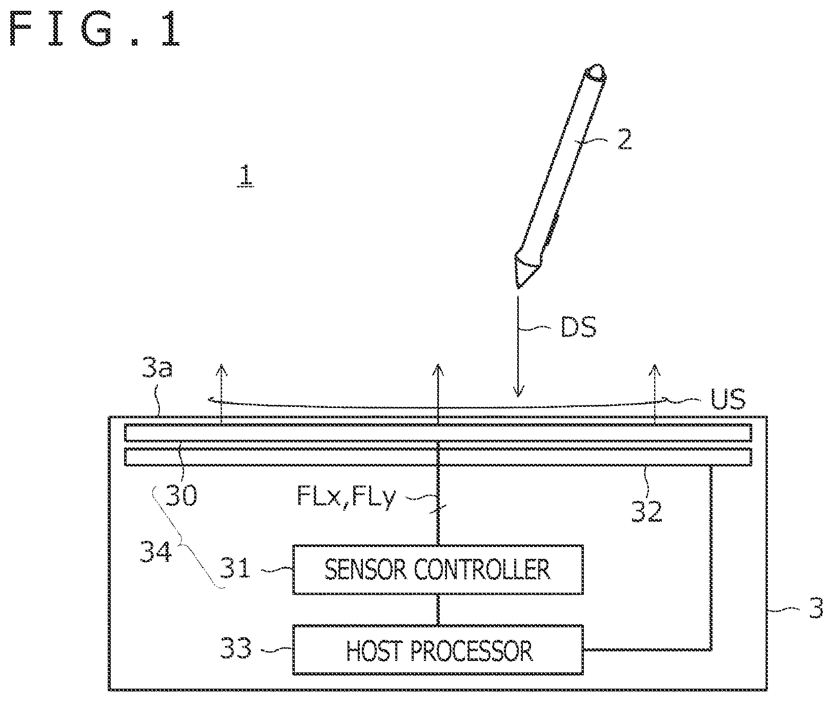
is a diagram illustrating the system configuration of a position detection system 1 according to a first embodiment of the present disclosure. As illustrated in this figure, the position detection system 1 includes a pen 2 and an electronic device 3 including a touch surface 3 a . The pen 2 is an active pen supporting an active capacitive coupling method. The electronic device 3 is, for example, a tablet-type computer and includes a sensor panel 30 , a sensor controller 31 , a display 32 , and a host processor 33 as illustrated in the figure.
The pen 2 is configured to receive an uplink signal US transmitted from the sensor controller 31 through the sensor panel 30 and transmit a downlink signal DS in response to the received uplink signal US. The uplink signal US is a signal transmitted by the sensor controller 31 periodically and has functions of notifying the pen 2 of transmission timing of the downlink signal DS and reception timing of a next uplink signal US and transmitting a command to the pen 2 . Receiving the uplink signal US, the pen 2 determines a transmission and reception schedule of the downlink signal DS and the next uplink signal US on the basis of reception timing of the uplink signal US, and transmits the downlink signal DS and receives the next uplink signal US according to the determined transmission and reception schedule. In addition, the pen 2 generates the downlink signal DS according to a command included in the uplink signal US.
The downlink signal DS is a signal including a position signal, which is an unmodulated carrier signal, and a data signal, which is a carrier signal modulated on the basis of data. The position signal is used for the sensor controller 31 to derive the position of the pen 2 . Meanwhile, the data signal is used to transmit given data from the pen 2 to the sensor controller 31 . Examples of the data transmitted by the data signal include a pen identifier (ID) assigned to the pen 2 in advance, a pen pressure value indicating the magnitude of pressure applied to a pen tip of the pen 2 , and information indicating the ON/OFF state of a switch provided on an external surface of the pen 2 .
The sensor panel 30 and the sensor controller 31 together form a position detection device 34 that detects the position of the pen 2 in the touch surface 3 a . Specifically, the sensor panel 30 is a rectangular member disposed under the touch surface 3 a , which is a flat surface, and includes a plurality of sensor electrodes. The sensor controller 31 is an integrated circuit individually connected to each of the sensor electrodes in the sensor panel 30 through a corresponding one of a plurality of FPC wires FLx and FLy disposed in flexible printed circuit boards. The sensor controller 31 performs a process of periodically transmitting the uplink signal US by using some or all of the sensor electrodes in the sensor panel 30 , and receiving the downlink signal DS transmitted by the pen 2 in response to the uplink signal US through the sensor panel 30 .
In the case where the position signal is received from the pen 2 undetected, the sensor controller 31 acquires a reception intensity of the position signal at each of all the sensor electrodes and derives a distribution curve of reception intensity from the result thereof, thereby deriving the position of the pen 2 in the touch surface 3 a (global scan). Meanwhile, in the case where the position signal is received from the pen 2 already detected, the sensor controller 31 acquires a reception intensity of the position signal at each of a specified number of sensor electrodes positioned in the vicinity of a position derived in the previous instance and derives a distribution curve of reception intensity from the result thereof, thereby updating the position of the pen 2 in the touch surface 3 a (local scan). In the case where the data signal is received from the pen 2 , the sensor controller 31 receives the data signal at one or a specified number of sensor electrodes positioned in the vicinity of the position derived in the previous instance and demodulates the data signal, thereby acquiring the data transmitted by the pen 2 . The sensor controller 31 is configured to supply the position derived and the data acquired in the above-described manners to the host processor 33 as often as necessary.
The host processor 33 is a central processing unit of the electronic device 3 and performs functions of executing an operating system of the electronic device 3 and various types of applications by reading and executing programs stored in a memory, which is not illustrated in the figure. The applications executed by the host processor 33 include a drawing application.
The drawing application is a program for causing the host processor 33 to perform a process of generating stroke data on the basis of positions and data sequentially supplied from the sensor controller 31 . Other processes that the drawing application causes the host processor 33 to perform include a process of storing the generated stroke data in the memory, a process of generating a video signal by subjecting the generated stroke data to rendering, and a process of supplying the generated video signal to the display 32 to display the generated stroke data on the display 32 .
The display 32 is a display device including a display panel having a plurality of pixels arranged in a matrix, and a drive circuit for driving the display panel to present a desired display. Specific examples of the display 32 include a liquid crystal display, an organic electroluminescence (EL) display, and an electronic paper. The drive circuit is configured to drive each pixel of the display panel according to the video signal supplied from the host processor 33 .
is a diagram illustrating the configuration of the position detection device 34 in detail. As illustrated in this figure, the sensor panel 30 includes, as the above-described plurality of sensor electrodes, a plurality of X electrodes 30 x each extending in a Y direction and arranged at regular intervals in an X direction perpendicular to the Y direction, and a plurality of Y electrodes 30 y each extending in the X direction and arranged at regular intervals in the Y direction. Note that, in and figures to be referenced later, only eight X electrodes 30 x (i.e., X electrodes 30 x 1 to 30 x 8 ) and eight Y electrodes 30 y (i.e., Y electrodes 30 y 1 to 30 y 8 ) are illustrated for simpler illustration, but in reality, more X electrodes 30 x and more Y electrodes 30 y are provided.
The sensor panel 30 is connected to the sensor controller 31 through three flexible printed circuit boards Fx, Fy 1 , and Fy 2 . A plurality of FPC wires FLx corresponding to the respective X electrodes 30 x are arranged to extend in the flexible printed circuit board Fx. Similarly, a plurality of FPC wires FLy corresponding to respective ones of some of the plurality of Y electrodes 30 y (specifically, the Y electrodes 30 y 1 to 30 y 4 ) are arranged to extend in the flexible printed circuit board Fy 1 , while a plurality of FPC wires FLy corresponding to respective ones of the rest of the plurality of Y electrodes 30 y (specifically, the Y electrodes 30 y 5 to 30 y 8 ) are arranged to extend in the flexible printed circuit board Fy 2 .
Each of the plurality of X electrodes 30 x is connected to the sensor controller 31 through a plurality of connection wires CLx. Each connection wire CLx includes a routing line RLx arranged to extend in the sensor panel 30 , and the above-described FPC wire FLx. An FPC terminal Tx for connecting the flexible printed circuit board Fx to the sensor panel 30 is disposed at a central portion of an end portion of the sensor panel 30 on one side in the Y direction, and the routing line RLx and the FPC wire FLx that form each connection wire CLx are connected to each other in the FPC terminal Tx. In addition, the routing line RLx of each connection wire CLx is connected to an end portion (i.e., an end portion on the side closer to the terminal Tx) of the corresponding X electrode 30 x on the one side in the Y direction. Hereinafter, the connection wires CLx connected to the X electrodes 30 x 1 to 30 x 8 will sometimes be referred to as connection wires CLx 1 to CLx 8 , respectively.
In addition, each of the plurality of Y electrodes 30 y is connected to the sensor controller 31 through a plurality of connection wires CLy. Each connection wire CLy includes a routing line RLy arranged to extend in the sensor panel 30 , and the above-described FPC wire FLy. FPC terminals Ty 1 and Ty 2 for connecting the flexible printed circuit boards Fy 1 and Fy 2 , respectively, to the sensor panel 30 are disposed at opposite end portions (i.e., on opposite sides of the FPC terminal Tx) of the end portion of the sensor panel 30 on the one side in the Y direction, and the routing line RLy and the FPC wire FLy that form each connection wire CLy are connected to each other in the FPC terminal Ty 1 or the FPC terminal Ty 2 . Hereinafter, the connection wires CLy connected to the Y electrodes 30 y 1 to 30 y 8 will sometimes be referred to as connection wires CLy 1 to CLy 8 , respectively.
Some of the plurality of connection wires CLy (specifically, the connection wires CLy 1 to CLy 4 ) are arranged to extend at regular intervals in a region A 1 (i.e., a first region) that lies over an end portion of the sensor panel 30 on one side in the X direction and the flexible printed circuit board Fy 1 , while the rest of the plurality of connection wires CLy (specifically, the connection wires CLy 5 to CLy 8 ) are arranged to extend at regular intervals in a region A 2 (i.e., a second region) that lies over an end portion of the sensor panel 30 on an opposite side in the X direction and the flexible printed circuit board Fy 2 . Each of the connection wires CLy arranged to extend in the region A 1 is connected to an end portion (i.e., an end portion on the side closer to the region A 1 ) of the corresponding Y electrode 30 y on the one side in the X direction. Meanwhile, each of the connection wires CLy arranged to extend in the region A 2 is connected to an end portion (i.e., an end portion on the side closer to the region A 2 ) of the corresponding Y electrode 30 y on the opposite side in the X direction.
In addition to the above-described rest of the plurality of connection wires CLy, two extension lines EX 1 and EX 3 are arranged to extend in the region A 2 . Similarly, in addition to the above-described some of the plurality of connection wires CLy, two extension lines EX 2 and EX 4 are arranged to extend in the region A 1 . The extension line EX 1 (i.e., a first extension line) is a wire connected to an end portion (i.e., an end portion on the side closer to the region A 2 ) of the Y electrode 30 y 4 (i.e., a first sensor electrode) on the opposite side in the X direction, and is arranged to extend along the connection wire CLy 5 (i.e., a second connection wire). The extension line EX 2 (i.e., a second extension line) is a wire connected to an end portion (i.e., an end portion on the side closer to the region A 1 ) of the Y electrode 30 y 5 (i.e., a second sensor electrode) on the one side in the X direction, and is arranged to extend along the connection wire CLy 4 (i.e., a first connection wire). The extension line EX 3 (i.e., a third extension line) is a wire connected to an end portion (i.e., an end portion on the side closer to the region A 2 ) of the Y electrode 30 y 3 (i.e., a third sensor electrode), which is adjacent to the Y electrode 30 y 5 with the Y electrode 30 y 4 intervening therebetween, on the opposite side in the X direction, and is arranged to extend along the extension line EX 1 . The extension line EX 4 (i.e., a fourth extension line) is a wire connected to an end portion (i.e., an end portion on the side closer to the region A 1 ) of the Y electrode 30 y 6 (i.e., a fourth sensor electrode), which is adjacent to the Y electrode 30 y 4 with the Y electrode 30 y 5 intervening therebetween, on the one side in the X direction, and is arranged to extend along the extension line EX 2 .
Through provision of the extension lines EX 1 to EX 4 , the sensor panel 30 and the position detection device 34 according to the present embodiment are able to minimize a reduction in accuracy in deriving the position which is caused by arranging the plurality of connection wires CLy to extend in the regions A 1 and A 2 in a distributed manner. This regard will now be described in detail below.
A, 3 B, and 3 C are diagrams schematically illustrating the distributions of coupling capacitance with the Y electrodes 30 y 4 , 30 y 5 , and 30 y 6 , respectively, as a center in a comparative example in which the extension lines EX 1 to EX 4 are eliminated from the sensor panel 30 illustrated in . Each Y electrode 30 y has coupling capacitance in relation to another Y electrode 30 y , and this coupling capacitance includes a component (i.e., a sensor electrode component) caused by direct adjacency with the other Y electrode 30 y , and a component (i.e., a connection wire component) caused by adjacency between the connection wire CLy connected to the Y electrode 30 y and another connection wire CLy.
First, referring to A , the Y electrode 30 y 4 has a connection wire component of coupling capacitance in relation to each of the Y electrodes 30 y 2 and 30 y 3 , but does not have a connection wire component of coupling capacitance in relation to either of the Y electrodes 30 y 5 and 30 y 6 . This is because the connection wires CLy 2 to CLy 4 are arranged to extend in the region A 1 while the connection wires CLy 5 and CLy 6 are arranged to extend in the region A 2 .
Next, referring to B , the Y electrode 30 y 5 has a connection wire component of coupling capacitance in relation to each of the Y electrodes 30 y 6 and 30 y 7 , but does not have a connection wire component of coupling capacitance in relation to either of the Y electrodes 30 y 3 and 30 y 4 . This is because the connection wires CLy 5 to CLy 7 are arranged to extend in the region A 2 while the connection wires CLy 3 and CLy 4 are arranged to extend in the region A 1 .
Next, referring to C , the Y electrode 30 y 6 has a connection wire component of coupling capacitance in relation to each of the Y electrodes 30 y 5 to 30 y 8 , but does not have a connection wire component of coupling capacitance in relation to the Y electrode 30 y 4 . This is because the connection wires CLy 5 to CLy 8 are arranged to extend in the region A 2 while the connection wire CLy 4 is arranged to extend in the region A 1 .
As will be understood by comparing A to 3 C with one another, the distributions of coupling capacitance with the Y electrodes 30 y 4 , 30 y 5 , and 30 y 6 , respectively, as the center are significantly different from one another due to differences in the connection wire components of coupling capacitance. Such differences in the distribution of coupling capacitance between the Y electrodes 30 y cause a distortion of the above-described distribution curve (i.e., the distribution curve of reception intensity of the position signal), resulting in reduced accuracy of the position derivation by the sensor controller 31 .
D, 3 E, and 3 F are diagrams schematically illustrating the distributions of coupling capacitance with the Y electrodes 30 y 4 , 30 y 5 , and 30 y 6 , respectively, as a center according to the present embodiment. In the present embodiment, the above-described provision of the extension lines EX 1 to EX 4 causes additional coupling capacitance between the Y electrodes 30 y . Thus, in D to 3 F , in addition to the sensor electrode components and the connection wire components illustrated in A to 3 C , additional components of coupling capacitance caused by the extension lines EX 2 and EX 4 in the region A 1 (i.e., additional components caused by the extension lines in the region A 1 ) and additional components of coupling capacitance caused by the extension lines EX 1 and EX 3 in the region A 2 (i.e., additional components caused by the extension lines in the region A 2 ) are illustrated.
First, referring to D , the connection wire CLy 4 connected to the Y electrode 30 y 4 is adjacent to the extension lines EX 2 and EX 4 in the region A 1 as illustrated in . As a result, additional components caused by the extension lines in the region A 1 are added to the coupling capacitance in relation to each of the Y electrodes 30 y 5 and 30 y 6 . Meanwhile, the extension line EX 1 connected to the Y electrode 30 y 4 is adjacent to the extension line EX 3 and the connection wires CLy 5 and CLy 6 in the region A 2 . As a result, additional components caused by the extension lines in the region A 2 are added to the coupling capacitance in relation to each of the Y electrodes 30 y 3 , 30 y 5 , and 30 y 6 .
Next, referring to E , the connection wire CLy 5 connected to the Y electrode 30 y 5 is adjacent to the extension lines EX 1 and EX 3 in the region A 2 . As a result, additional components caused by the extension lines in the region A 2 are added to the coupling capacitance in relation to each of the Y electrodes 30 y 3 and 30 y 4 . Meanwhile, the extension line EX 2 connected to the Y electrode 30 y 5 is adjacent to the connection wires CLy 3 and CLy 4 and the extension line EX 4 in the region A 1 . As a result, additional components caused by the extension lines in the region A 1 are added to the coupling capacitance in relation to each of the Y electrodes 30 y 3 , 30 y 4 , and 30 y 6 .
Next, referring to F , the connection wire CLy 6 connected to the Y electrode 30 y 6 is adjacent to the extension line EX 1 in the region A 2 . As a result, an additional component caused by the extension line in the region A 2 is added to the coupling capacitance in relation to the Y electrode 30 y 4 . Meanwhile, the extension line EX 4 connected to the Y electrode 30 y 6 is adjacent to the connection wire CLy 4 and the extension line EX 2 in the region A 1 . As a result, additional components caused by the extension lines in the region A 1 are added to the coupling capacitance in relation to each of the Y electrodes 30 y 4 and 30 y 5 .
As will be understood by comparing D to 3 F with A to 3 C , the position detection device 34 according to the present embodiment achieves a reduction in the differences between the distributions of coupling capacitance with the Y electrodes 30 y 4 , 30 y 5 , and 30 y 6 , respectively, as the center when compared to the comparative example. This leads to a reduced distortion of the above-described distribution curve (i.e., the distribution curve of reception intensity of the position signal) when compared to the comparative example, and it can therefore be said that the sensor panel 30 and the position detection device 34 according to the present embodiment are able to minimize the reduction in accuracy in deriving the position which is caused by arranging the plurality of connection wires CLy to extend in the regions A 1 and A 2 in a distributed manner.
As described above, the sensor panel 30 and the position detection device 34 according to the present embodiment are able to cause the distribution of coupling capacitance with each Y electrode 30 y as the center to fall within a substantially fixed range, and are therefore able to minimize the reduction in accuracy in deriving the position which is caused by arranging the connection wires CLy to extend in the regions A 1 and A 2 in a distributed manner.
Note that, while the four extension lines EX 1 to EX 4 are disposed in the sensor panel 30 in the present embodiment described above, only the extension lines EX 1 and EX 2 may be disposed while the extension lines EX 3 and EX 4 are omitted. Also note that more than four extension lines may be disposed therein. Also note that the length of each extension line is not limited to the length thereof illustrated in , and should be determined such that the distribution of coupling capacitance with each Y electrode 30 y as the center can fall within a substantially fixed range. These regards apply to first and second modifications described below as well.
is a diagram illustrating the configuration of a position detection device 34 according to a first modification of the present embodiment in detail. The position detection device 34 according to the present modification is different from the position detection device 34 according to the present embodiment in the configuration concerning the plurality of connection wires CLx, and is otherwise similar to the position detection device 34 according to the present embodiment. Note that, while part of the configuration concerning the plurality of connection wires CLy is not illustrated in , the omitted part of the configuration is the same as illustrated in . The following description is provided with a focus placed on differences from the position detection device 34 according to the present embodiment.
The present modification corresponds to a case where the FPC terminal Tx needs to be divided into two FPC terminals Tx 1 and Tx 2 because, for example, the number of X electrodes 30 x is great. A sensor panel 30 according to the present modification is connected to a sensor controller 31 through a flexible printed circuit board Fx that branches out into two parts on the side closer to the sensor panel 30 . Hereinafter, one of the two parts branching out from the flexible printed circuit board Fx which is connected to the FPC terminal Tx 1 will be referred to as a flexible printed circuit board Fx 1 (i.e., a first flexible printed circuit board), while the other part, which is connected to the FPC terminal Tx 2 , will be referred to as a flexible printed circuit board Fx 2 (i.e., a second flexible printed circuit board).
Some of the plurality of connection wires CLx (specifically, the connection wires CLx 1 to CLx 4 ) are arranged to extend at regular intervals in a region A 3 (i.e., the first region) that lies over the FPC terminal Tx 1 and the flexible printed circuit board Fx 1 , while the rest of the plurality of connection wires CLx (specifically, the connection wires CLx 5 to CLx 8 ) are arranged to extend at regular intervals in a region A 4 (i.e., the second region) that lies over the FPC terminal Tx 2 and the flexible printed circuit board Fx 2 .
In addition to the above-described rest of the plurality of connection wires CLx, two extension lines EX 5 and EX 7 are arranged to extend in the region A 4 . Similarly, in addition to the above-described some of the plurality of connection wires CLx, two extension lines EX 6 and EX 8 are arranged to extend in the region A 3 . Here, the flexible printed circuit board Fx is a multi-layer board, and the extension lines EX 5 to EX 8 are arranged to extend in layers different from a layer in which each of the connection wires CLx 1 to CLx 8 extends. This is an arrangement to prevent a contact between the extension lines EX 5 to EX 8 and the connection wires CLx 1 to CLx 8 except through via hole conductors VC, which will be described below. In addition, the extension lines EX 5 and EX 7 and the extension lines EX 6 and EX 8 are also arranged to extend in mutually different layers to prevent a contact therebetween.
The extension line EX 5 (i.e., the first extension line) is a wire connected to the connection wire CLx 4 through a via hole conductor VC arranged to pass from layer to layer, and is arranged to extend along the connection wire CLx 5 (i.e., the second connection wire). The extension line EX 6 (i.e., the second extension line) is a wire connected to the connection wire CLx 5 through a via hole conductor VC, and is arranged to extend along the connection wire CLx 4 (i.e., the first connection wire). The extension line EX 7 (i.e., the third extension line) is a wire connected to the connection wire CLx 3 through a via hole conductor VC, and is arranged to extend along the extension line EX 5 . The extension line EX 8 (i.e., the fourth extension line) is a wire connected to the connection wire CLx 6 through a via hole conductor VC, and is arranged to extend along the extension line EX 6 .
The above-described configuration enables the sensor panel 30 and the position detection device according to the present modification to cause the distribution of coupling capacitance with each X electrode 30 x as the center to fall within a substantially fixed range for the same reason as in the present embodiment. This in turn makes it possible to minimize a reduction in accuracy in deriving a position which is caused by arranging the connection wires CLx to extend in the regions A 3 and A 4 in a distributed manner.
is a diagram illustrating the configuration of a position detection device 34 according to a second modification of the present embodiment in detail. The position detection device 34 according to the present modification is also different from the position detection device 34 according to the present embodiment in the configuration concerning the plurality of connection wires CLx, and is otherwise similar to the position detection device 34 according to the present embodiment. Note that, while part of the configuration concerning the plurality of connection wires CLy is not illustrated in , the omitted part of the configuration is the same as illustrated in . The following description is provided with a focus placed on differences from the position detection device 34 according to the present embodiment.
The present modification corresponds to a case where a flexible printed circuit board connected to a sensor controller 31 needs to be divided into two boards because, for example, the number of X electrodes 30 x is great. A sensor panel 30 according to the present modification is connected to the sensor controller 31 through a flexible printed circuit board Fx that branches out into two parts on the side closer to the sensor controller 31 . Hereinafter, one of the two parts branching out from the flexible printed circuit board Fx will be referred to as a flexible printed circuit board Fx 3 (i.e., the first flexible printed circuit board), while the other part will be referred to as a flexible printed circuit board Fx 4 (i.e., the second flexible printed circuit board).
Some of the plurality of connection wires CLx (specifically, the connection wires CLx 1 to CLx 4 ) are arranged to extend at regular intervals in a region A 5 (i.e., the first region) that lies in the flexible printed circuit board Fx 3 , while the rest of the plurality of connection wires CLx (specifically, the connection wires CLx 5 to CLx 8 ) are arranged to extend at regular intervals in a region A 6 (i.e., the second region) that lies in the flexible printed circuit board Fx 4 .
In addition to the above-described rest of the plurality of connection wires CLx, two extension lines EX 9 and EX 11 are arranged to extend in the region A 6 . Similarly, in addition to the above-described some of the plurality of connection wires CLx, two extension lines EX 10 and EX 12 are arranged to extend in the region A 5 . In the present modification as well, the flexible printed circuit board Fx is a multi-layer board, and the extension lines EX 9 to EX 12 are arranged to extend in layers different from a layer in which each of the connection wires CLx 1 to CLx 8 extends. In addition, the extension lines EX 9 and EX 11 and the extension lines EX 10 and EX 12 are also arranged to extend in mutually different layers to prevent a contact therebetween.
The extension line EX 9 (i.e., the first extension line) is a wire connected to the connection wire CLx 4 through a via hole conductor VC, and is arranged to extend along the connection wire CLx 5 (i.e., the second connection wire). The extension line EX 10 (i.e., the second extension line) is a wire connected to the connection wire CLx 5 through a via hole conductor VC, and is arranged to extend along the connection wire CLx 4 (i.e., the first connection wire). The extension line EX 11 (i.e., the third extension line) is a wire connected to the connection wire CLx 3 through a via hole conductor VC, and is arranged to extend along the extension line EX 9 . The extension line EX 12 (i.e., the fourth extension line) is a wire connected to the connection wire CLx 6 through a via hole conductor VC, and is arranged to extend along the extension line EX 10 .
The above-described configuration enables the sensor panel 30 and the position detection device according to the present modification to cause the distribution of coupling capacitance with each X electrode 30 x as the center to fall within a substantially fixed range for the same reason as in the present embodiment and the first modification. This in turn makes it possible to minimize a reduction in accuracy in deriving a position which is caused by arranging the connection wires CLx to extend in the regions A 5 and A 6 in a distributed manner.
Next, a position detection system 1 according to a second embodiment of the present disclosure will be described below. The position detection system 1 according to the present embodiment is different from the position detection system 1 according to the first embodiment in that dummy lines that are not connected to any sensor electrode are provided in place of the extension lines connected to the sensor electrodes and in processes performed by the sensor controller 31 , and is similar to the position detection system 1 according to the first embodiment in other respects including the system configuration illustrated in . The following description is provided with a focus placed on differences from the position detection system 1 according to the first embodiment.
is a diagram illustrating the configuration of a position detection device 34 according to the present embodiment in detail. To compare this figure with , the position detection device 34 according to the present embodiment is different from the position detection device 34 according to the first embodiment in including dummy lines DM 1 and DM 2 and not including the extension lines EX 1 to EX 4 .
The dummy line DM 1 (i.e., a first dummy line) is a wire arranged to extend along a connection wire CLy 4 (i.e., the first connection wire) in a region A 1 , and includes a routing line formed in a sensor panel 30 and an FPC wire formed in a flexible printed circuit board Fy 1 . The routing line and the FPC wire that form the dummy line DM 1 are connected to each other in an FPC terminal Ty 1 .
The dummy line DM 2 (i.e., a second dummy line) is a wire arranged to extend along a connection wire CLy 5 (i.e., the second connection wire) in a region A 2 , and includes a routing line formed in the sensor panel 30 and an FPC wire formed in a flexible printed circuit board Fy 2 . The routing line and the FPC wire that form the dummy line DM 2 are connected to each other in an FPC terminal Ty 2 .
Each of the dummy lines DM 1 and DM 2 is connected to the sensor controller 31 , but is not connected to any of a plurality of X electrodes 30 x and a plurality of Y electrodes 30 y . The sensor controller 31 according to the present embodiment is configured to derive a distribution curve of reception intensity employing the above-described differential method, and employs the dummy lines DM 1 and DM 2 when deriving a differential between a reception intensity at the Y electrode 30 y 4 and a reception intensity at the Y electrode 30 y 5 . The processes performed by the sensor controller 31 will be described in detail below. Processes performed by a sensor controller 31 in related art and a problem thereof are first described with reference to A, 7 B, and 7 C , and processes performed by the sensor controller 31 according to the present embodiment are then described with reference to .
A to 7 C are each a diagram illustrating a circuit provided in the sensor controller 31 in related art. A represents a circuit for deriving a differential between a reception intensity at the Y electrode 30 y 3 and a reception intensity at the Y electrode 30 y 4 , B represents a circuit for deriving a differential between a reception intensity at the Y electrode 30 y 4 and a reception intensity at the Y electrode 30 y 5 , and C represents a circuit for deriving a differential between a reception intensity at the Y electrode 30 y 5 and a reception intensity at the Y electrode 30 y 6 . While not illustrated in the figures, circuits for deriving differentials between reception intensities at other sensor electrodes have similar configurations.
Referring to A , for example, the sensor controller 31 includes a two-input subtraction circuit DO having an inverting input terminal connected to the connection wire CLy 3 and a non-inverting input terminal connected to the connection wire CLy 4 . A signal supplied from the connection wire CLy 3 to the sensor controller 31 includes a signal component S 30y3 and a noise component N 30y3 received at the Y electrode 30 y 3 , and a noise component N CLy3 received at the connection wire CLy 3 connected to the Y electrode 30 y 3 . Similarly, a signal supplied from the connection wire CLy 4 to the sensor controller 31 includes a signal component S 30y4 and a noise component N 30y4 received at the Y electrode 30 y 4 , and a noise component N CLy4 received at the connection wire CLy 4 connected to the Y electrode 30 y 4 .
Here, because the Y electrode 30 y 3 and the Y electrode 30 y 4 are adjacent to each other, the noise component N 30y3 and the noise component N 30y4 can be considered to have the same value. Similarly, because the connection wire CLy 3 and the connection wire CLy 4 are adjacent to each other, the noise component N CLy3 and the noise component N CLy4 can also be considered to have the same value. Accordingly, when a differential between the signal supplied from the Y electrode 30 y 4 to the sensor controller 31 and the signal supplied from the Y electrode 30 y 3 to the sensor controller 31 is derived, the four noise components N 30y3 , N CLy3 , N 30y4 , and N CLy4 are canceled out as illustrated in A , leaving only a differential, S 30y4 S 30y3 , between the signal components.
The above regard basically applies to the differentials between reception intensities at other sensor electrodes as well except that, as illustrated in B , a noise component N Cly5 -N CLy4 is left in the differential between the reception intensity at the Y electrode 30 y 4 and the reception intensity at the Y electrode 30 y 5 . This is because the connection wire CLy 4 and the connection wire CLy 5 are not adjacent to each other as a result of the plurality of connection wires CLy being arranged in the regions A 1 and A 2 in a distributed manner. The noise component left in the differential between the reception intensities causes a distortion in a derived distribution curve, leading to reduced accuracy of position derivation by the sensor controller 31 .
is a diagram illustrating a circuit provided in the sensor controller 31 according to the present embodiment. While only a circuit for deriving the differential between the reception intensity at the Y electrode 30 y 4 and the reception intensity at the Y electrode 30 y 5 is illustrated in this figure, circuits for deriving differentials between reception intensities at other sensor electrodes have a configuration similar to the configuration illustrated in A and 7 C .
As illustrated in , the sensor controller 31 includes two two-input subtraction circuits D 1 a and D 1 b provided in a stage previous to a subtraction circuit DO. An inverting input terminal of the subtraction circuit D 1 a is connected to the dummy line DM 1 , a non-inverting input terminal thereof is connected to the connection wire CLy 4 , and an output terminal thereof is connected to an inverting input terminal of the subtraction circuit DO. Meanwhile, an inverting input terminal of the subtraction circuit D 1 b is connected to the dummy line DM 2 , a non-inverting input terminal thereof is connected to the connection wire CLy 5 , and an output terminal thereof is connected to a non-inverting input terminal of the subtraction circuit DO.
A signal supplied from the dummy line DM 1 to the sensor controller 31 includes a noise component N DM1 received at the dummy line DM 1 . Here, as illustrated in , the dummy line DM 1 is arranged to extend along the connection wire CLy 4 , and therefore, the noise component N CLy4 and the noise component N DM1 can be considered to have the same value. Accordingly, an output signal (i.e., a first differential signal) outputted from the subtraction circuit D 1 a corresponds to S 30y4 +N 30y4 . Similarly, a signal supplied from the dummy line DM 2 to the sensor controller 31 includes a noise component N DM2 received at the dummy line DM 2 . Then, because the dummy line DM 2 is arranged to extend along the connection wire CLy 5 , the noise component N CLy5 and the noise component N DM2 can be considered to have the same value. Therefore, an output signal (i.e., a second differential signal) outputted from the subtraction circuit D 1 b corresponds to S 30y5 +N 30y5 .
Moreover, because the Y electrode 30 y 4 and the Y electrode 30 y 5 are adjacent to each other, the noise component N 30y4 and the noise component N 30y5 can be considered to have the same value, and therefore, a signal S 30y5 +S 30y4 , with the noise components N 30y4 and N 30y5 eliminated therefrom, is outputted from an output terminal of the subtraction circuit DO. That is, the position detection device 34 according to the present embodiment is able to eliminate the noise components even from the differential between the reception intensity at the Y electrode 30 y 4 and the reception intensity at the Y electrode 30 y 5 , and is therefore able to minimize a reduction in accuracy in deriving a position which is caused by arranging the plurality of connection wires CLy to extend in the regions A 1 and A 2 in a distributed manner.
As described above, the position detection device 34 according to the present embodiment enables external noises to be canceled out even between the Y electrodes 30 y 4 and 30 y 5 , which are adjacent to each other but the respective connection wires CLy connected to which are arranged separately in the regions A 1 and A 2 . Accordingly, when differentials between reception intensities are derived employing the differential method, external noises can be canceled out, and this makes it possible to minimize a reduction in accuracy in deriving a position which is caused by arranging the connection wires CLy to extend in the regions A 1 and A 2 in a distributed manner.
Note that, while the subtraction circuits are provided in the sensor controller 31 in the above-described present embodiment, it is to be appreciated that subtractions of signals may be performed by digital processing instead of by employing physical subtraction circuits.
is a diagram illustrating a circuit provided in a sensor controller 31 according to a first modification of the present embodiment. The circuit illustrated in this figure is an example modification of the circuit illustrated in . Circuits for deriving differentials between reception intensities at other sensor electrodes have a configuration similar to the configuration illustrated in A and 7 C .
The sensor controller 31 according to the present modification is different from the sensor controller 31 according to the present embodiment in using a single four-input subtraction circuit D 2 in place of the subtraction circuits DO, D 1 a , and D 1 b . The subtraction circuit D 2 has two inverting input terminals and two non-inverting input terminals, and the two inverting input terminals are connected to the respective dummy lines DM 1 and DM 2 , while the two non-inverting input terminals are connected to the respective connection wires CLy 4 and CLy 5 . A signal outputted from the subtraction circuit D 2 corresponds to S 30y4 +N 30y4 +N CLy4 +S 30y5 +N 30y5 +N CLy5 −N DM1 +N DM2 , but because the noise component N CLy4 and the noise component N DM1 , the noise component Nuys and the noise component N DM2 , and the noise component N 30y4 and the noise component N 30y5 can be considered to have the same values as described above, all the noise components are eliminated, and a signal actually outputted corresponds to S 30y5 −S 30y4 . This result is the same as in the case of the example illustrated in . Therefore, similarly to the position detection device 34 according to the present embodiment, a position detection device 34 according to the present modification is also able to minimize a reduction in accuracy in deriving a position which is caused by arranging the connection wires CLy to extend in the regions A 1 and A 2 in a distributed manner.
is a diagram illustrating the configuration of a position detection device 34 according to a second modification of the present embodiment in detail. The position detection device 34 according to the present modification is different from the position detection device 34 according to the present embodiment in that a plurality of connection wires CLy are collectively arranged to extend in a single region while a plurality of connection wires CLx are arranged to extend in two regions in a distributed manner, and in that dummy lines DM 3 and DM 4 are provided in place of the dummy lines DM 1 and DM 2 , and is otherwise similar to the position detection device 34 according to the present embodiment. The following description is provided with a focus placed on differences from the position detection device 34 according to the present embodiment.
A sensor panel 30 according to the second modification of the present embodiment is connected to a sensor controller 31 through three flexible printed circuit boards Fx 1 , Fx 2 , and Fy. A plurality of FPC wires FLy corresponding to respective Y electrodes 30 y are arranged to extend in the flexible printed circuit board Fy. Meanwhile, a plurality of FPC wires FLx corresponding to respective ones of some of a plurality of X electrodes 30 x (specifically, X electrodes 30 x 1 to 30 x 4 ) are arranged to extend in the flexible printed circuit board Fx 1 (i.e., the first flexible printed circuit board), while a plurality of FPC wires FLx corresponding to respective ones of the rest of the plurality of X electrodes 30 x (specifically, X electrodes 30 x 5 to 30 x 8 ) are arranged to extend in the flexible printed circuit board Fx 2 (i.e., the second flexible printed circuit board).
The flexible printed circuit boards Fx 1 , Fx 2 , and Fy are connected to FPC terminals Tx 1 , Tx 2 , and Ty, respectively, of the sensor panel 30 . The FPC terminals Tx 1 , Tx 2 , and Ty are arranged in this order from the one side in the X direction in the vicinity of a side that forms an end of the sensor panel 30 on the one side in the Y direction.
A routing line RLy and an FPC wire FLy that form each connection wire CLy are connected to each other in the FPC terminal Ty. In addition, the routing line RLy of each connection wire CLy is connected to an end portion of the corresponding Y electrode 30 y on the opposite side in the X direction.
Some of the plurality of connection wires CLx which are connected to the above-described some of the plurality of X electrodes 30 x are arranged to extend at regular intervals in a region A 3 (i.e., the first region) that lies over an area in the vicinity of the FPC terminal Tx 1 and the flexible printed circuit board Fx 1 , while the rest of the plurality of connection wires CLx are arranged to extend at regular intervals in a region A 4 (i.e., the second region) that lies over an area in the vicinity of the FPC terminal Tx 2 and the flexible printed circuit board Fx 2 .
The dummy line DM 3 (i.e., the first dummy line) is a wire arranged to extend along the connection wire CLx 4 (i.e., the first connection wire) in the region A 3 , and includes a routing line formed in the sensor panel 30 and an FPC wire formed in the flexible printed circuit board Fx 1 . The routing line and the FPC wire that form the dummy line DM 3 are connected to each other in the FPC terminal Tx 1 .
The dummy line DM 4 (i.e., the second dummy line) is a wire arranged to extend along the connection wire CLx 5 (i.e., the second connection wire) in the region A 4 , and includes a routing line formed in the sensor panel 30 and an FPC wire formed in the flexible printed circuit board Fx 2 . The routing line and the FPC wire that form the dummy line DM 4 are connected to each other in the FPC terminal Tx 2 .
Similarly to the dummy lines DM 1 and DM 2 according to the present embodiment, each of the dummy lines DM 3 and DM 4 is connected to the sensor controller 31 , but is not connected to any of the plurality of X electrodes 30 x and the plurality of Y electrodes 30 y . The sensor controller 31 employs the dummy lines DM 3 and DM 4 when deriving a differential between a reception intensity at the X electrode 30 x 4 and a reception intensity at the X electrode 30 x 5 . Specifically, the differential between the reception intensity at the X electrode 30 x 4 and the reception intensity at the X electrode 30 x 5 is derived employing a circuit similar to the circuit described above with reference to or . Noise components are thus eliminated from the differential between the reception intensity at the X electrode 30 x 4 and the reception intensity at the X electrode 30 x 5 , and therefore, the position detection device 34 according to the present modification is able to minimize a reduction in accuracy in deriving a position which is caused by arranging the plurality of connection wires CLx to extend in the regions A 3 and A 4 in a distributed manner.
Note that, while the plurality of connection wires CLy are collectively arranged to extend in the single region in the above-described present modification, it is to be appreciated that the configuration of the plurality of connection wires CLy may be the same as that according to the present embodiment illustrated in . Also note that, while the flexible printed circuit boards Fx 1 and Fx 2 are completely separate from each other in the above-described present modification, it is to be appreciated that the flexible printed circuit boards Fx 1 and Fx 2 may be branching portions of a single flexible printed circuit board Fx as in the example illustrated in , for example.
is a diagram illustrating the configuration of a position detection device 34 according to a third modification of the present embodiment in detail. The position detection device 34 according to the present modification is different from the position detection device 34 according to the second modification in that dummy lines DM 5 and DM 6 are additionally provided and in processes performed by the sensor controller 31 , and is otherwise similar to the position detection device 34 according to the second modification. The following description is provided with a focus placed on differences from the position detection device 34 according to the second modification.
The dummy line DM 5 (i.e., a third dummy line) is a wire arranged to extend along the connection wire CLx 1 in the region A 3 , and includes a routing line formed in the sensor panel 30 and an FPC wire formed in the flexible printed circuit board Fx 1 . The routing line and the FPC wire that form the dummy line DM 5 are connected to each other in the FPC terminal Tx 1 .
The dummy line DM 6 (i.e., a fourth dummy line) is a wire arranged to extend along the connection wire CLx 8 in the region A 4 , and includes a routing line formed in the sensor panel 30 and an FPC wire formed in the flexible printed circuit board Fx 2 . The routing line and the FPC wire that form the dummy line DM 6 are connected to each other in the FPC terminal Tx 2 .
Similarly to the dummy lines DM 3 and DM 4 , each of the dummy lines DM 5 and DM 6 is connected to the sensor controller 31 , but is not connected to any of the plurality of X electrodes 30 x and the plurality of Y electrodes 30 y . The sensor controller 31 employs the dummy line DM 5 when deriving a differential between a reception intensity at the X electrode 30 x 1 (i.e., the third sensor electrode), which is positioned at an end of the plurality of X electrodes 30 x on the one side, and a reception intensity at the X electrode 30 x 2 (i.e., the fourth sensor electrode), which is adjacent to the X electrode 30 x 1 , and employs the dummy line DM 6 when deriving a differential between a reception intensity at the X electrode 30 x 8 (i.e., a fifth sensor electrode), which is positioned at an end of the plurality of X electrodes 30 x on the opposite side, and a reception intensity at the X electrode 30 x 7 (i.e., a sixth sensor electrode), which is adjacent to the X electrode 30 x 8 . This regard will be described specifically below.
A and 12 B are each a diagram illustrating a circuit provided in the sensor controller 31 according to the present modification. A illustrates a circuit for deriving the differential between the reception intensity at the X electrode 30 x 1 and the reception intensity at the X electrode 30 x 2 , while B illustrates a circuit for deriving the differential between the reception intensity at the X electrode 30 x 7 and the reception intensity at the X electrode 30 x 8 . Circuits for deriving differentials between reception intensities at other sensor electrodes have configurations similar to those according to the present embodiment described above.
First, with reference to A , the sensor controller 31 has a two-input subtraction circuit D 3 provided in a stage previous to a subtraction circuit DO as illustrated in A and so on. An inverting input terminal of the subtraction circuit D 3 is connected to the dummy line DM 5 , a non-inverting input terminal thereof is connected to the connection wire CLx 1 (i.e., a third connection wire), and an output terminal thereof is connected to an inverting input terminal of the subtraction circuit DO. The connection wire CLx 2 (i.e., a fourth connection wire) is connected to a non-inverting input terminal of the subtraction circuit DO. As a result, a noise component N DM5 received at the dummy line DM 5 is supplied to the inverting input terminal of the subtraction circuit D 3 , while a signal component S 30x1 and a noise component N 30x1 received at the X electrode 30 x 1 and a noise component N CLx1 received at the connection wire CLx 1 are supplied to the non-inverting input terminal of the subtraction circuit D 3 . Accordingly, a signal (i.e., a third differential signal) outputted from the output terminal of the subtraction circuit D 3 and supplied to the inverting input terminal of the subtraction circuit DO corresponds to S 30x1 +N 30x1 +(N CLx1 −N DM5 ). Meanwhile, a signal component S 30x2 and a noise component N 30x2 received at the X electrode 30 x 2 and a noise component N CLx2 received at the connection wire CLx 2 are supplied to the non-inverting input terminal of the subtraction circuit DO.
Here, in the vicinity of an end portion of each of the sensor panel 30 and the flexible printed circuit boards Fx 1 and Fx 2 , noise that is different from noise that occurs at a middle portion thereof may occur. This case corresponds to a case in which N CLx2 =NC and N DM5 =NE, where NC denotes the noise that occurs at the middle portion and NE denotes the noise that occurs in the vicinity of the end portion. In this case, the noise component N CLx1 received at the connection wire CLx 1 , which is positioned at a boundary between the end and middle portions, amounts to NC+NE.
In the case where such noise occurs, the subtraction circuit D 3 performs a function of eliminating the noise NE, and an output signal outputted from the subtraction circuit D 3 , i.e., a signal inputted to the inverting input terminal of the subtraction circuit DO, corresponds to S 30x1 +N 30x1 +NC. Meanwhile, a signal inputted to the non-inverting input terminal of the subtraction circuit DO corresponds to S 30x2 +N 30x2 +NC. Accordingly, an output signal outputted from the subtraction circuit DO corresponds to S 30x2 +N 30x2 +NC−(S 30x1 +N 30x1 +NC)=S 30x2 +S 30x1 , with the noises NC and NE and the respective external noises received at the X electrodes 30 x 1 and 30 x 2 eliminated therefrom.
Next, with reference to B , the sensor controller 31 has a two-input subtraction circuit D 3 provided in a stage previous to a subtraction circuit DO in this case as well. An inverting input terminal of the subtraction circuit D 3 is connected to the dummy line DM 6 , a non-inverting input terminal thereof is connected to the connection wire CLx 8 (i.e., a fifth connection wire), and an output terminal thereof is connected to a non-inverting input terminal of the subtraction circuit DO. The connection wire CLx 7 (i.e., a sixth connection wire) is connected to an inverting input terminal of the subtraction circuit DO. As a result, a noise component N DM6 received at the dummy line DM 6 is supplied to the inverting input terminal of the subtraction circuit D 3 , while a signal component S 30x8 and a noise component N 30x8 received at the X electrode 30 x 8 and a noise component N CLx8 received at the connection wire CLx 8 are supplied to the non-inverting input terminal of the subtraction circuit D 3 . Accordingly, a signal (i.e., a fourth differential signal) outputted from the output terminal of the subtraction circuit D 3 and supplied to the non-inverting input terminal of the subtraction circuit DO corresponds to S 30x8 +N 30x8 +(N CLx8 −N DM6 ). Meanwhile, a signal component S 30x7 and a noise component N 30x7 received at the X electrode 30 x 7 and a noise component N CLx7 received at the connection wire CLx 7 are supplied to the inverting input terminal of the subtraction circuit DO. The above configuration makes it possible to eliminate the noises NC and NE and the respective external noises received at the X electrodes 30 x 7 and 30 x 8 from an output signal outputted from the subtraction circuit DO as in the case of A .
As described above, even if, in the vicinity of the end portion of each of the sensor panel 30 and the flexible printed circuit boards Fx 1 and Fx 2 , noise that is different from the noise that occurs at the middle portion thereof occurs, the position detection device 34 according to the present modification is able to eliminate such noise from the output signal outputted from the subtraction circuit DO. Therefore, the position detection device 34 according to the present modification is able to minimize a reduction in accuracy in deriving a position which is caused as a result of, in the vicinity of the end portion of each of the sensor panel 30 and the flexible printed circuit boards Fx 1 and Fx 2 , the noise that is different from the noise that occurs at the middle portion thereof occurring.
While preferred embodiments of the present disclosure have been described above, the present disclosure is not limited to the above-described embodiments, and it is to be appreciated that various other embodiments of the present disclosure can be implemented without departing from the gist of the present disclosure.
For example, even in the first embodiment, the sensor controller 31 may be configured to employ the differential method to derive the distribution curve. Also, the position detection device 34 may be provided with both the extension lines as used in the first embodiment or the modifications thereof and the dummy lines as used in the second embodiment or the modifications thereof, and be configured to cause the sensor controller 31 to perform the processes as described above with respect to the second embodiment or the modifications thereof.
Also, in each of the above-described embodiments, each of the routing lines RLx and RLy is arranged to extend in a straight fashion, but some or all of the routing lines RLx and RLy, especially the routing lines RLy in the region A 2 illustrated in , may be arranged to extend in a step-like fashion. This could prevent the formation of the extension lines EX 1 and EX 3 from causing an increase in the area of the region A 2 .
Figures (11)
Citations
This patent cites (17)
- US8704796
- US10725600
- US10782836
- US20170031514
- US20170097529
- US20170177120
- US20180239476
- US20190212836
- US20200089343
- US20200104027
- US20200201509
- US20220147166
- US2011-227793
- US2014-170334
- US2015-026343
- US2020-119356
- US2019/026649