Abstract
According to one embodiment, an optical control device includes a first liquid crystal cell and a second liquid crystal cell. The second liquid crystal cell is stacked on the first liquid crystal cell. The first liquid crystal cell has a function of modulating and converting a first polarization component of incident light into a second polarization component, and hardly modulating and converting a third polarization component of incident light into a fourth polarization component. The second liquid crystal cell has a function of hardly modulating the second polarization component transmitted through the first liquid crystal cell, and modulating the fourth polarization component transmitted through the first liquid crystal cell.
Claims (15)
1. An optical control device comprising: a first liquid crystal cell comprising a first substrate comprising a plurality of first control electrodes, a second substrate, and a first liquid crystal layer twisted and aligned between the first substrate and the second substrate; and a second liquid crystal cell comprising a third substrate comprising a plurality of second control electrodes, a fourth substrate, and a second liquid crystal layer twisted and aligned between the third substrate and the fourth substrate, wherein the second liquid crystal cell is stacked on the first liquid crystal cell, the first control electrode overlaps the second control electrode, the first liquid crystal cell has a function of modulating and converting a first polarization component of incident light into a second polarization component, and hardly modulating and converting a third polarization component of incident light into a fourth polarization component, the second liquid crystal cell has a function of hardly modulating the second polarization component transmitted through the first liquid crystal cell, and modulating the fourth polarization component transmitted through the first liquid crystal cell, and the plurality of first control electrodes and the plurality of second control electrodes are arranged spaced apart in a first direction and elongated in a second direction intersecting the first direction.
10. An optical control device comprising: a first liquid crystal cell comprising a first substrate comprising a plurality of first control electrodes, a second substrate, and a first liquid crystal layer twisted and aligned between the first substrate and the second substrate; and a second liquid crystal cell comprising a third substrate comprising a plurality of second control electrodes, a fourth substrate, and a second liquid crystal layer twisted and aligned between the third substrate and the fourth substrate, wherein the second liquid crystal cell is stacked on the first liquid crystal cell, the first control electrode overlaps the second control electrode, the first liquid crystal cell has a function of modulating and converting a first polarization component of incident light into a second polarization component, and hardly modulating and converting a third polarization component of incident light into a fourth polarization component, the second liquid crystal cell has a function of hardly modulating the second polarization component transmitted through the first liquid crystal cell, and modulating the fourth polarization component transmitted through the first liquid crystal cell, the first substrate further comprises a first common electrode located between adjacent first control electrodes, the first control electrodes and the first common electrode are located in a same layer, the third substrate further comprises a second common electrode located between adjacent second control electrodes, the second control electrodes and the second common electrode are located in a same layer, and the first common electrode overlaps the second common electrode.
13. An optical control device comprising: a first liquid crystal cell comprising a first substrate comprising a plurality of first control electrodes, a second substrate, and a first liquid crystal layer twisted and aligned between the first substrate and the second substrate; and a second liquid crystal cell comprising a third substrate comprising a plurality of second control electrodes, a fourth substrate, and a second liquid crystal layer twisted and aligned between the third substrate and the fourth substrate, wherein the second liquid crystal cell is stacked on the first liquid crystal cell, the first control electrode overlaps the second control electrode, the first liquid crystal cell has a function of modulating and converting a first polarization component of incident light into a second polarization component, and hardly modulating and converting a third polarization component of incident light into a fourth polarization component, the second liquid crystal cell has a function of hardly modulating the second polarization component transmitted through the first liquid crystal cell, and modulating the fourth polarization component transmitted through the first liquid crystal cell, the first substrate further comprises a first common electrode located between adjacent first control electrodes; and a first insulating film located between the first control electrodes and the first common electrode, the third substrate further comprises a second common electrode located between adjacent second control electrodes, and a second insulating film located between the second control electrodes and the second common electrode, and the first common electrode overlaps the second common electrode.
Show 12 dependent claims
2. The optical control device according to claim 1 , wherein the first liquid crystal cell and the second liquid crystal cell have a same optical rotatory power, the second polarization component and the third polarization component have a same polarization plane, and the first polarization component and the fourth polarization component have a same polarization plane.
3. The optical control device according to claim 1 , wherein a width of the first control electrode is equal to a width of the second control electrode, and an interval between the first control electrodes is equal to an interval between the second control electrodes.
4. The optical control device according to claim 3 , wherein the first liquid crystal cell has a first modulation area provided with the plurality of first control electrodes, the second liquid crystal cell has a second modulation area provided with the plurality of second control electrodes, and the first modulation area and the second modulation area have a same shape and are formed in a rectangular shape.
5. The optical control device according to claim 4 , wherein the second substrate comprises a first common electrode opposed to the plurality of first control electrodes, and the fourth substrate comprises a second common electrode opposed to the plurality of second control electrodes.
6. The optical control device according to claim 5 , further comprising an adhesive layer that is transparent and bonds the first substrate and the third substrate.
7. The optical control device according to claim 6 , wherein the second substrate and the fourth substrate are each in contact with an air layer.
8. The optical control device according to claim 5 , further comprising an adhesive layer that is transparent and bonds the second substrate and the third substrate.
9. The optical control device according to claim 8 , wherein the first substrate and the fourth substrate are each in contact with an air layer.
11. The optical control device according to claim 10 , further comprising: an adhesive layer that is transparent and bonds the first liquid crystal cell and the second liquid crystal cell; and an ultraviolet absorbing layer provided on at least one of an outer surface of the first liquid crystal cell and an outer surface of the second liquid crystal cell, wherein the ultraviolet absorbing layer is a transparent conductive layer.
12. The optical control device according to claim 10 , further comprising: an adhesive layer that is transparent and bonds the first substrate and the third substrate; a first ultraviolet absorbing layer provided on an outer surface of the second substrate; and a second ultraviolet absorbing layer provided on an outer surface of the fourth substrate, wherein each of the first ultraviolet absorbing layer and the second ultraviolet absorbing layer is a transparent conductive layer.
14. The optical control device according to claim 13 , further comprising: an adhesive layer that is transparent and bonds the first liquid crystal cell and the second liquid crystal cell; and an ultraviolet absorbing layer provided on at least one of an outer surface of the first liquid crystal cell and an outer surface of the second liquid crystal cell, wherein the ultraviolet absorbing layer is a transparent conductive layer.
15. The optical control device according to claim 13 , further comprising: an adhesive layer that is transparent and bonds the first substrate and the third substrate; a first ultraviolet absorbing layer provided on an outer surface of the second substrate; and a second ultraviolet absorbing layer provided on an outer surface of the fourth substrate, wherein each of the first ultraviolet absorbing layer and the second ultraviolet absorbing layer is a transparent conductive layer.
Full Description
Show full text →
CROSS-REFERENCE TO RELATED APPLICATIONS
This application is a Continuation Application of PCT Application No. PCT/JP2020/029048, filed Jul. 29, 2020 and based upon and claiming the benefit of priority from Japanese Patent Application No. 2019-174015, filed Sep. 25, 2019, the entire contents of all of which are incorporated herein by reference.
FIELD
The embodiment of the present invention relates to an optical control device.
BACKGROUND
In recent years, an optical control device using a liquid crystal cell has been proposed. Such an optical control device primarily converges or diverges a light beam of one polarization component. For example, an optical control device is disclosed in which two liquid crystal cells are stacked, one polarization component is modulated in one liquid crystal cell, and the other polarization component is modulated in the other liquid crystal cell.
BRIEF DESCRIPTION OF THE DRAWINGS
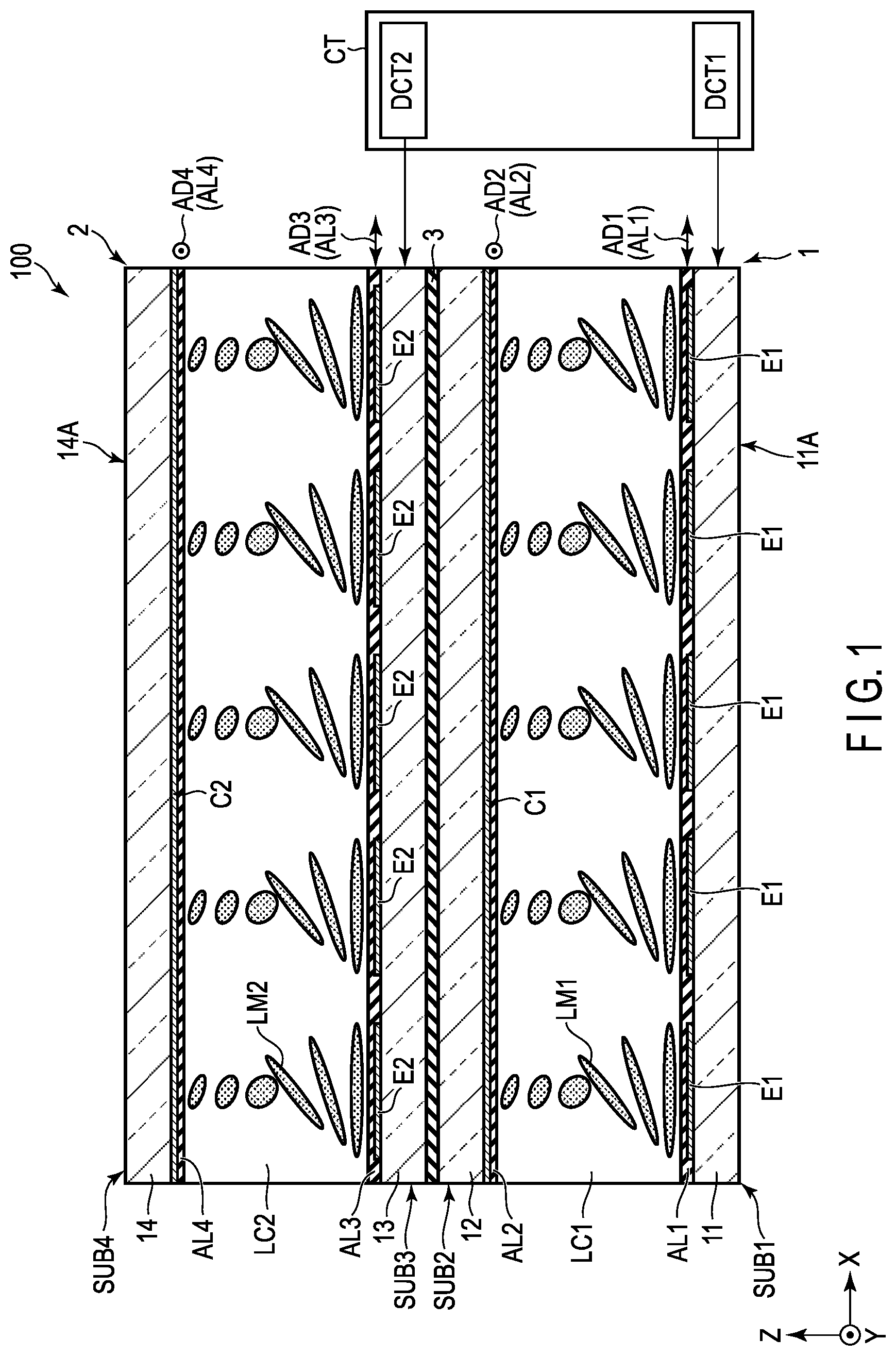
is a diagram showing a configuration example of an optical control device 100 according to one embodiment.
is a cross-sectional diagram showing a configuration example of a first liquid crystal cell 1 .
is an exploded perspective diagram showing a main part of the optical control device 100 .
is a diagram for describing a liquid crystal lens LL 1 formed in the first liquid crystal cell 1 .
is a diagram for describing functions of liquid crystal lenses LL 1 and LL 2 by the optical control device 100 .
is a diagram for describing functions of liquid crystal lenses LL 1 and LL 2 by the optical control device 100 .
is a cross-sectional diagram showing another configuration example of the optical control device 100 .
is a diagram showing another configuration example of the optical control device 100 according to one embodiment.
is a diagram for describing the liquid crystal lens LL 1 formed in the first liquid crystal cell 1 shown in .
is a diagram showing another configuration example of the optical control device 100 according to one embodiment.
is a diagram showing another shape of a first control electrode E 1 .
is a diagram showing another shape of the first control electrode E 1 .
is a cross-sectional diagram showing another configuration example of the optical control device 100 .
DETAILED DESCRIPTION
In general, according to one embodiment, an optical control device includes a first liquid crystal cell including a first substrate including a plurality of first control electrodes, a second substrate, and a first liquid crystal layer twisted and aligned between the first substrate and the second substrate, and a second liquid crystal cell including a third substrate including a plurality of second control electrodes, a fourth substrate, and a second liquid crystal layer twisted and aligned between the third substrate and the fourth substrate. The second liquid crystal cell is stacked on the first liquid crystal cell. The first control electrode overlaps the second control electrode. The first liquid crystal cell has a function of modulating and converting a first polarization component of incident light into a second polarization component, and hardly modulating and converting a third polarization component of incident light into a fourth polarization component. The second liquid crystal cell has a function of hardly modulating the second polarization component transmitted through the first liquid crystal cell, and modulating the fourth polarization component transmitted through the first liquid crystal cell.
According to one embodiment, it is possible to provide an optical control device that can be manufactured at low cost.
Embodiments will be described hereinafter with reference to the accompanying drawings. The disclosure is merely an example, and proper changes within the spirit of the invention, which are easily conceivable by a skilled person, are included in the scope of the invention as a matter of course. In addition, in some cases, in order to make the description clearer, the widths, thicknesses, shapes, etc., of the respective parts are schematically illustrated in the drawings, compared to the actual modes. However, the schematic illustration is merely an example, and adds no restrictions to the interpretation of the invention. Besides, in the specification and drawings, the same or similar elements as or to those described in connection with preceding drawings or those exhibiting similar functions are denoted by like reference numerals, and a detailed description thereof is omitted unless otherwise necessary.
is a diagram showing a configuration example of an optical control device 100 according to one embodiment. For example, a first direction X, a second direction Y and a third direction Z are orthogonal to each other, but they may intersect at an angle other than 90 degrees. In the following descriptions, viewing from above downward onto an X-Y plane defined by the first direction X and the second direction Y is referred to as planar view.
The optical control device 100 includes a first liquid crystal cell 1 , a second liquid crystal cell 2 , and a control unit CT. The first liquid crystal cell 1 and the second liquid crystal cell 2 have substantially the same component.
The first liquid crystal cell 1 includes a first substrate SUB 1 , a second substrate SUB 2 , and a first liquid crystal layer LC 1 . The first substrate SUB 1 includes an insulating substrate 11 , a plurality of first control electrodes E 1 provided on the insulating substrate 11 , and an alignment film AL 1 covering the first control electrodes E 1 . The second substrate SUB 2 includes an insulating substrate 12 , a first common electrode C 1 provided on the insulating substrate 12 , and an alignment film AL 2 covering the first common electrode C 1 . The first common electrode C 1 is opposed to the plurality of first control electrodes E 1 .
The second liquid crystal cell 2 includes a third substrate SUB 3 , a fourth substrate SUB 4 , and a second liquid crystal layer LC 2 . The third substrate SUB 3 includes an insulating substrate 13 , a plurality of second control electrodes E 2 provided on the insulating substrate 13 , and an alignment film AL 3 covering the second control electrodes E 2 . The second control electrode E 2 is formed so as to overlap the first control electrode E 1 in the third direction Z. The fourth substrate SUB 4 includes an insulating substrate 14 , a second common electrode C 2 provided on the insulating substrate 14 , and an alignment film AL 4 covering the second common electrode C 2 . The second common electrode C 2 is opposed to the plurality of second control electrodes E 2 .
The insulating substrates 11 to 14 are, for example, transparent substrates such as glass substrates and resin substrates.
The first control electrode E 1 , the second control electrode E 2 , the first common electrode C 1 , and the second common electrode C 2 are transparent electrodes formed of a transparent conductive material such as indium tin oxide (ITO) or indium zinc oxide (IZO).
The alignment films AL 1 to AL 4 are horizontal alignment films having an alignment restriction force approximately parallel to an X-Y plane. For example, an alignment treatment direction AD 1 of the alignment film AL 1 and an alignment treatment direction AD 3 of the alignment film AL 3 are both parallel to the first direction X. In addition, an alignment treatment direction AD 2 of the alignment film AL 2 and an alignment treatment direction AD 4 of the alignment film AL 4 are both parallel to the second direction Y. In other words, the alignment treatment direction AD 1 is orthogonal to the alignment treatment direction AD 2 in the first liquid crystal cell 1 , and the alignment treatment direction AD 3 is orthogonal to the alignment treatment direction AD 4 in the second liquid crystal cell 2 . Incidentally, the alignment treatment may be rubbing treatment or optical alignment treatment.
The first liquid crystal layer LC 1 is held by the alignment films AL 1 and AL 2 between the first substrate SUB 1 and the second substrate SUB 2 , and includes liquid crystal molecules LM 1 that are twisted and aligned at 90 degrees. Similarly, the second liquid crystal layer LC 2 is held by the alignment films AL 3 and AL 4 between the third substrate SUB 3 and the fourth substrate SUB 4 , and includes liquid crystal molecules LM 2 that are twisted and aligned at 90 degrees. These first liquid crystal layer LC 1 and second liquid crystal layer LC 2 have, for example, positive dielectric anisotropy.
The second liquid crystal cell 2 is stacked on the first liquid crystal cell 1 in the third direction Z. The insulating substrate 12 and the insulating substrate 13 are bonded to each other with a transparent adhesive layer 3 . The refractive index of the adhesive layer 3 is equal to the refractive indexes of the insulating substrates 12 and 13 . In contrast, an outer surface 11 A of the insulating substrate 11 and an outer surface 14 A of the insulating substrate 14 are each in contact with an air layer.
The control unit CT includes voltage controllers DCT 1 and DCT 2 . The voltage controller DCT 1 controls voltages to be applied to the first control electrode E 1 and the first common electrode C 1 in the first liquid crystal cell 1 . The voltage controller DCT 2 controls voltages to be applied to the second control electrode E 2 and the second common electrode C 2 in the second liquid crystal cell 2 .
Such optical control device 100 is combined with, for example, a light source that emits non-polarized light, and is installed so that the outer surface 11 A serves as an entrance surface of light. The first liquid crystal cell 1 has a function of modulating and converting a first polarization component of incident light into a second polarization component, and hardly modulating and converting a third polarization component of incident light into a fourth polarization component. The second liquid crystal cell 2 has a function of hardly modulating the second polarization component transmitted through the first liquid crystal cell 1 , but modulating the fourth polarization component transmitted through the first liquid crystal cell 1 . The functions of the first liquid crystal cell 1 and the second liquid crystal cell 2 will be described in detail later.
The modulation herein refers to converging or diverging a polarization component transmitted through a liquid crystal layer by a refractive index distribution type lens (hereinafter, referred to as a liquid crystal lens) formed in the liquid crystal layer. In other words, the first liquid crystal cell 1 converges or diverges the first polarization component, and the second liquid crystal cell 2 converges or diverges the fourth polarization component. In the first liquid crystal cell 1 , the third polarization component is hardly converged or diverged, and similarly, in the second liquid crystal cell 2 , the second polarization component is hardly converged or diverged. A degree of convergence or divergence (modulation rate) is controlled by the voltage applied to the liquid crystal layer. In other words, the modulation rate of the first polarization component in the first liquid crystal cell 1 is controlled by the voltage controller DCT 1 , and the modulation rate of the fourth polarization component in the second liquid crystal cell 2 is controlled by the voltage controller DCT 2 .
As described above, the first liquid crystal cell 1 and the second liquid crystal cell 2 have substantially the same components and have the same optical rotatory power. In the present embodiment, each of the first liquid crystal cell 1 and the second liquid crystal cell 2 has an optical rotatory power to rotate a polarization plane of the incident polarization component (linearly polarized light) by 90 degrees. In other words, the polarization plane of the first polarization component is orthogonal to the polarization plane of the second polarization component, and the polarization plane of the third polarization component is orthogonal to the polarization plane of the fourth polarization component. When the first polarization component and the third polarization component are orthogonal to each other, the first polarization component and the fourth polarization component have the same polarization plane, and the second polarization component and the third polarization component have the same polarization plane.
is a cross-sectional diagram showing a configuration example of the first liquid crystal cell 1 . Although the first liquid crystal cell 1 will be described here, the second liquid crystal cell 2 also has the same cross-sectional structure as the first liquid crystal cell 1 , and the description thereof will be omitted.
In the first substrate SUB 1 , the plurality of first control electrodes E 1 are arranged spaced apart in the first direction X in a first modulation area A 11 . A feed line PL is provided in a peripheral area A 12 outside the first modulation area A 11 . The plurality of first control electrodes E 1 and the feed line PL are electrically connected to the voltage controller DCT 1 shown in .
In the second substrate SUB 2 , the first common electrode C 1 is, for example, a single plate electrode that is located on substantially the entire surface of the first modulation area A 11 and also partially extends to the peripheral area A 12 . In the first modulation area A 11 , the first common electrode C 1 is opposed to the plurality of first control electrodes E 1 through the first liquid crystal layer LC 1 . In the peripheral area A 12 , the first common electrode C 1 is opposed to the feed line PL.
In the peripheral area A 12 , the first substrate SUB 1 and the second substrate SUB 2 are bonded together with a sealant SE. The sealant SE includes a conducting material CD. The conducting material CD is interposed between the feed line PL and the first common electrode C 1 and electrically connects the feed line PL and the first common electrode C 1 .
is an exploded perspective diagram showing a main part of the optical control device 100 . Incidentally, the first common electrode C 1 overlapping the first modulation area A 11 and the second common electrode C 2 overlapping the second modulation area A 21 are indicated by dotted lines. In the first modulation area A 11 , the plurality of first control electrodes E 1 are arranged spaced apart at regular intervals D 1 in the first direction X. Each of the first control electrodes E 1 is, for example, a strip electrode elongated in the second direction Y. Each of the first control electrodes E 1 has the same width W 1 along the first direction X. In a second modulation area A 21 , the plurality of second control electrodes E 2 are arranged spaced apart at regular intervals D 2 in the first direction X. Each of the second control electrodes E 2 is, for example, a strip electrode elongated in the second direction Y. Each of the second control electrodes E 2 has the same width W 2 along the first direction X. The width W 1 is equal to the width W 2 , and the interval D 1 is equal to the interval D 2 . In other words, the plurality of first control electrodes E 1 overlap the plurality of second control electrodes E 2 , respectively, in planar view. The widths W 1 and W 2 and the intervals D 1 and D 2 are, for example, from 10 μm to 30 μm.
In the example shown in , the first modulation area A 11 and the second modulation area A 21 are formed in a rectangular shape extending in the first direction X, but may be formed in a rectangular shape extending in the second direction Y, or may be formed in a circular shape, an elliptical shape, or other shapes. The first modulation area A 11 and the second modulation area A 21 have the same shape and overlap each other in planar view.
is a diagram for describing a liquid crystal lens LL 1 formed in the first liquid crystal cell 1 . In , only configurations necessary for description are shown. Although not described, a liquid crystal lens LL 2 similar to the liquid crystal lens LL 1 to be described with reference to can also be formed in the second liquid crystal cell 2 .
(A) of shows an off state (OFF) in which no potential difference is generated between the first control electrodes E 11 to E 15 and the first common electrode C 1 . The liquid crystal molecules LM 1 included in the first liquid crystal layer LC 1 are twisted and aligned by alignment restriction forces of the alignment films AL 1 and AL 2 .
(B) of shows an on state (ON) in which a potential difference is formed between the first control electrodes E 11 to E 15 and the first common electrode C 1 . The voltage controller DCT 1 supplies a predetermined voltage to each of the first control electrodes E 11 to E 15 and the first common electrode C 1 . The first liquid crystal layer LC 1 has positive dielectric anisotropy as described above. For this reason, in a state where an electric field is formed, the liquid crystal molecules LM 1 are aligned so that their major axes are along the electric field. For example, the first control electrodes E 11 , E 12 , E 13 , E 14 , and E 15 are supplied with voltages of 7V, 3V, 0V, 3V, and 7V, respectively, and the first common electrode C 1 is supplied with a voltage of 0V.
Since an electric field along the third direction Z is formed in an area where each of the first control electrodes E 11 and E 15 is opposed to the first common electrode C 1 , the liquid crystal molecules LM 1 are aligned so that their major axes are along the third direction Z. In an area where the first control electrode E 13 is opposed to the first common electrode C 1 , almost no electric field is formed, and the liquid crystal molecules LM 1 are maintained in the initial alignment state (twisted alignment state). In an area where the first control electrode E 12 is opposed to the first common electrode C 1 , an intermediate alignment state between an area where the first control electrode E 11 is opposed to the first common electrode C 1 and an area where the first control electrode E 13 is opposed to the first common electrode C 1 is formed. In an area where the first control electrode E 14 is opposed to the first common electrode C 1 , an intermediate alignment state between an area where the first control electrode E 15 is opposed to the first common electrode C 1 and an area where the first control electrode E 13 is opposed to the first common electrode C 1 is formed.
The liquid crystal molecules LM 1 have refractive anisotropy Δn. For this reason, the first liquid crystal layer LC 1 has a refractive index distribution according to the alignment state of the liquid crystal molecules LM 1 . Alternatively, the first liquid crystal layer LC 1 has a retardation distribution or a phase distribution represented by Δn·d, where d is a thickness of the first liquid crystal layer LC 1 along the third direction Z. Incidentally, the thickness d is, for example, from 10 μm to 50 μm. The liquid crystal lens LL 1 indicated by dotted lines in the drawing is formed by such a refractive index distribution, a retardation distribution, or a phase distribution. The liquid crystal lens LL 1 thus shown functions as a convex lens.
Next, functions of the liquid crystal lenses LL 1 and LL 2 by the optical control device 100 will be described with reference to . In the following description, when the traveling direction of light is along the third direction Z, linearly polarized light having a polarization plane along the first direction X is referred to as first polarized light (P-polarized light) POL 1 , and linearly polarized light having a polarization plane along the second direction Y is referred to as second polarized light (S-polarized light) POL 2 . A light source LS emits non-polarized light including the first polarized light POL 1 and the second polarized light POL 2 . The first liquid crystal cell 1 is located between the light source LS and the second liquid crystal cell 2 .
As shown in , the first polarized light (first polarization component) POL 1 is converged by the liquid crystal lens LL 1 in the first liquid crystal cell 1 , and a polarization plane of the first polarized light POL 1 is rotated by 90 degrees to be converted into the second polarized light (second polarization component) POL 2 . The second polarized light POL 2 transmitted through the first liquid crystal cell 1 is transmitted through the second liquid crystal cell 2 without being converged by the liquid crystal lens LL 2 , and a polarization plane of the second polarized light POL 2 is rotated by 90 degrees to be converted into the first polarized light POL 1 . In other words, of the light emitted from the light source LS, the first polarized light POL 1 is converged by the optical control device 100 .
As shown in , the second polarized light (third polarization component) POL 2 is transmitted through the first liquid crystal cell 1 without being converged by the liquid crystal lens LL 1 , and the polarization plane of the second polarized light POL 2 is rotated by 90 degrees to be converted into the first polarized light (fourth polarization component) POL 1 . The first polarized light POL 1 transmitted through the first liquid crystal cell 1 is transmitted through the second liquid crystal cell 2 being converged by the liquid crystal lens LL 2 , and the polarization plane of the first polarized light POL 1 is rotated by 90 degrees to be converted into the second polarized light POL 2 . In other words, of the light emitted from the light source LS, the second polarized light POL 2 is converged by the optical control device 100 .
According to such optical control device 100 , the first liquid crystal cell 1 for modulating the first polarized light POL 1 and the second liquid crystal cell 2 for modulating the second polarized light POL 2 can be configured with the same specification. For this reason, regardless of the shape of the modulation area, by stacking the first liquid crystal cell 1 and the second liquid crystal cell 2 , the optical control device 100 that modulates (converges or diverges) light can be provided. In addition, according to the present embodiment, as compared with a case where the first liquid crystal cell 1 and the second liquid crystal cell 2 are configured with different specifications, it is possible to integrate the manufacturing line, thereby allowing the optical control device 100 to be manufactured at low cost.
is a cross-sectional diagram showing another configuration example of the optical control device 100 . The configuration example shown in is different from the configuration example shown in in that the first substrate SUB 1 and the third substrate SUB 3 are bonded with the transparent adhesive layer 3 . The second substrate SUB 2 and the fourth substrate SUB 4 are each in contact with the air layer. More specifically, the adhesive layer 3 bonds the insulating substrate 11 and the insulating substrate 13 . The refractive index of the adhesive layer 3 is equal to the refractive indexes of the insulating substrates 11 and 13 . In contrast, an outer surface 12 A of the insulating substrate 12 and the outer surface 14 A of the insulating substrate 14 are each in contact with the air layer.
The first common electrode C 1 is provided on an inner surface 12 B of the insulating substrate 12 , and the second common electrode C 2 is provided on an inner surface 14 B of the insulating substrate 14 . In other words, in the optical control device 100 , the first liquid crystal layer LC 1 and the second liquid crystal layer LC 2 are located between the first common electrode C 1 and the second common electrode C 2 that are plate electrodes. For example, the first common electrode C 1 and the second common electrode C 2 formed of ITO are conductive layers and function as an ultraviolet absorbing layer.
According to this configuration example, the same effect as in the above configuration example can be obtained. In addition, ultraviolet rays incident from the outer surface 12 A are absorbed by the first common electrode C 1 , and ultraviolet rays incident from the outer surface 14 A are absorbed by the second common electrode C 2 . Therefore, deterioration of the first liquid crystal layer LC 1 and the second liquid crystal layer LC 2 due to the ultraviolet rays is suppressed.
The second substrate SUB 2 is discharged via the first common electrode C 1 , and the fourth substrate SUB 4 is discharged via the second common electrode C 2 . Therefore, in the first liquid crystal layer LC 1 and the second liquid crystal layer LC 2 , alignment failure of the liquid crystal molecules caused by undesirable charging is suppressed.
is a diagram showing another configuration example of the optical control device 100 of the present embodiment. The configuration example shown in is different from the configuration example shown in in that in the first liquid crystal cell 1 , the first substrate SUB 1 includes the first control electrode E 1 and the first common electrode C 1 , and the first common electrode C 1 is located between adjacent first control electrodes E 1 . The first control electrode E 1 and the first common electrode C 1 are located in the same layer. For example, the first control electrode E 1 and the first common electrode C 1 are provided on the insulating substrate 11 and covered with the alignment film AL 1 . The first control electrode E 1 and the first common electrode C 1 are formed of, for example, the same transparent conductive material. Incidentally, in the example shown, one first control electrode E 1 is disposed between adjacent first common electrodes C 1 . However, a plurality of first control electrodes E 1 may be disposed between adjacent first common electrodes C 1 , or a plurality of first common electrodes C 1 may be disposed between adjacent first control electrodes E 1 .
Also, in the second liquid crystal cell 2 , similarly to the first liquid crystal cell 1 , the third substrate SUB 3 includes the second control electrode E 2 and the second common electrode C 2 . The second common electrode C 2 is located between adjacent second control electrodes E 2 . In addition, the second control electrode E 2 and the second common electrode C 2 are located in the same layer.
The width of the first common electrode C 1 is equal to the width W 2 of the second common electrode C 2 , and the interval between the first control electrode E 1 and the first common electrode C 1 is equal to the interval between the second control electrode E 2 and the second common electrode C 2 . The second control electrode E 2 is located directly above the first control electrode E 1 , and the second common electrode C 2 is located directly above the first common electrode C 1 . In other words, in planar view, the plurality of first control electrodes E 1 overlap the plurality of second control electrodes E 2 , and the plurality of first common electrodes C 1 overlap the plurality of second common electrodes C 2 .
The first liquid crystal cell 1 and the second liquid crystal cell 2 are bonded to each other with the transparent adhesive layer 3 . In the example shown, the second substrate SUB 2 and the third substrate SUB 3 are bonded to each other with the adhesive layer 3 . The refractive index of the adhesive layer 3 is equal to the refractive indexes of the insulating substrates 12 and 13 . In contrast, the outer surfaces of the insulating substrates 11 and 14 are each in contact with the air layer. No electrode is provided on the second substrate SUB 2 and the fourth substrate SUB 4 . In particular, from the viewpoint of suppressing the incidence of ultraviolet rays from the fourth substrate SUB 4 , an ultraviolet absorbing layer may be provided on the outer surface of the fourth substrate SUB 4 (or the outer surface of the insulating substrate 14 ). A specific example of the ultraviolet absorbing layer will be described later with reference to .
is a diagram for describing the liquid crystal lens LL 1 formed in the first liquid crystal cell 1 shown in . In , only configurations necessary for description are shown. Although not described, the liquid crystal lens LL 2 similar to the liquid crystal lens LL 1 to be described with reference to can also be formed in the second liquid crystal cell 2 .
(A) of shows an off state (OFF) in which no potential difference is generated between the first control electrode E 1 and the first common electrode C 1 . The liquid crystal molecules LM 1 included in the first liquid crystal layer LC 1 are twisted and aligned by alignment restriction forces of the alignment films AL 1 and AL 2 .
(B) of shows an on state (ON) in which a potential difference is formed between the first control electrode E 1 and the first common electrode C 1 . The voltage controller DCT 1 supplies a predetermined voltage to each of the first control electrode E 1 and the first common electrode C 1 . In a state where an electric field is formed, the liquid crystal molecules LM 1 are aligned so that their major axes are along the electric field. As a result, the liquid crystal lens LL 1 as indicated by dotted lines in the drawing is formed.
Also in the configuration examples shown in , the same effect as in the above configuration example can be obtained. In addition, in this configuration example, the feed line PL and the conducting material CD as described with reference to are unnecessary, and the configuration can be simplified. Incidentally, in the configuration examples shown in , similar to the configuration example shown in , the first substrate SUB 1 and the third substrate SUB 3 may be bonded with the transparent adhesive layer 3 .
is a diagram showing another configuration example of the optical control device 100 of the present embodiment. The configuration example shown in is different from the configuration example shown in in that the first substrate SUB 1 includes an insulating film (first insulating film) IL 1 located between the first control electrode E 1 and the first common electrode C 1 . In other words, it is different in that the first control electrode E 1 is located in a layer different from the first common electrode C 1 . For example, the first common electrode C 1 is provided on the insulating substrate 11 and covered with the insulating film IL 1 . The first control electrode E 1 is located on the insulating film IL 1 and is covered with the alignment film AL 1 . The first common electrode C 1 is located between adjacent first control electrodes E 1 .
Also, in the second liquid crystal cell 2 , similarly to the first liquid crystal cell 1 , the third substrate SUB 3 includes an insulating film (second insulating film) IL 2 located between the second control electrode E 2 and the second common electrode C 2 . For example, the second common electrode C 2 is provided on the insulating substrate 13 and covered with the insulating film IL 2 . The second control electrode E 2 is located on the insulating film IL 2 and is covered with the alignment film AL 3 . The second common electrode C 2 is located between adjacent second control electrodes E 2 .
The width of the first common electrode C 1 is equal to the width W 2 of the second common electrode C 2 , and the interval between the first control electrode E 1 and the first common electrode C 1 is equal to the interval between the second control electrode E 2 and the second common electrode C 2 . The second control electrode E 2 is located directly above the first control electrode E 1 , and the second common electrode C 2 is located directly above the first common electrode C 1 . In other words, in planar view, the plurality of first control electrodes E 1 overlap the plurality of second control electrodes E 2 , and the plurality of first common electrodes C 1 overlap the plurality of second common electrodes C 2 .
The second substrate SUB 2 and the third substrate SUB 3 are bonded to each other with the transparent adhesive layer 3 . The refractive index of the adhesive layer 3 is equal to the refractive indexes of the insulating substrates 12 and 13 . In contrast, the outer surfaces of the insulating substrates 11 and 14 are each in contact with the air layer. No electrode is provided on the second substrate SUB 2 and the fourth substrate SUB 4 . In particular, from the viewpoint of suppressing the incidence of ultraviolet rays from the fourth substrate SUB 4 , an ultraviolet absorbing layer may be provided on the outer surface of the fourth substrate SUB 4 (or the outer surface of the insulating substrate 14 ). A specific example of the ultraviolet absorbing layer will be described later with reference to .
Also in the configuration example shown in , the same effect as in the configuration example shown in can be obtained. In addition, since the first control electrode E 1 and the first common electrode C 1 to which different voltages are supplied are provided with the insulating film IL 1 interposed therebetween, intervals between the electrodes arranged in the same layer are widened, which can improve yields. Incidentally, in the configuration example shown in , similar to the configuration example shown in , the first substrate SUB 1 and the third substrate SUB 3 may be bonded with the transparent adhesive layer 3 .
The first control electrode E 1 and the second control electrode E 2 , and the first common electrode C 1 and the second common electrode C 2 described with reference to may be the strip electrodes described with reference to , or may have other shapes. Examples of other shapes will be described below.
In the example shown in , the first control electrode E 1 is formed in a substantially circular dot shape. The first common electrode C 1 is formed in an annular shape surrounding each of the plurality of first control electrodes E 1 . The plurality of first control electrodes E 1 and the first common electrode C 1 are each electrically connected to the voltage controller DCT 1 . For example, a lens array can be formed by forming an electric field between each of the first control electrodes E 1 and the first common electrode C 1 .
In the example shown in , the plurality of first control electrodes E 1 are formed in a concentric circle shape. The plurality of first control electrodes E 1 are each electrically connected to the voltage controller DCT 1 . For example, a circular lens can be formed by controlling voltage supplied to each of the first control electrodes E 1 .
is a cross-sectional diagram showing another configuration example of the optical control device 100 . The configuration example shown in is different from the configuration examples shown in in that the first substrate SUB 1 and the third substrate SUB 3 are bonded with the transparent adhesive layer 3 . The second substrate SUB 2 and the fourth substrate SUB 4 are located on the side opposite to the adhesive layer 3 . A first ultraviolet absorbing layer 21 is provided on an outer surface of the first liquid crystal cell 1 (or an outer surface of the second substrate SUB 2 ), and a second ultraviolet absorbing layer 22 is provided on an outer surface of the second liquid crystal cell 2 (or an outer surface of the fourth substrate SUB 4 ). More specifically, the first ultraviolet absorbing layer 21 is provided on the outer surface 12 A of the insulating substrate 12 , and the second ultraviolet absorbing layer 22 is provided on the outer surface 14 A of the insulating substrate 14 . In other words, in the optical control device 100 , the first liquid crystal layer LC 1 and the second liquid crystal layer LC 2 are located between the first ultraviolet absorbing layer 21 and the second ultraviolet absorbing layer 22 . The first ultraviolet absorbing layer 21 and the second ultraviolet absorbing layer 22 are transparent conductive layers formed of, for example, ITO.
According to this configuration example, the same effect as in the configuration example described with reference to can be obtained. In other words, ultraviolet rays incident from the second substrate SUB 2 side on which no electrode is provided are absorbed by the first ultraviolet absorbing layer 21 . In addition, ultraviolet rays incident from the fourth substrate SUB 4 side on which no electrode is provided are absorbed by the second ultraviolet absorbing layer 22 . Therefore, deterioration of the first liquid crystal layer LC 1 and the second liquid crystal layer LC 2 due to the ultraviolet rays is suppressed.
Incidentally, in the configuration example shown in , the first control electrode E 1 and the first common electrode C 1 of the first substrate SUB 1 are located in the same layer, but the first control electrode E 1 may be located in a layer different from the first common electrode C 1 . Similarly, the second control electrode E 2 and the second common electrode C 2 of the third substrate SUB 3 are located in the same layer, but the second control electrode E 2 may be located in a layer different from the second common electrode C 2 .
As described above, according to the present embodiment, it is possible to provide an optical control device that can be manufactured at low cost.
While certain embodiments have been described, these embodiments have been presented by way of example only, and are not intended to limit the scope of the inventions. Indeed, the novel embodiments described herein may be embodied in a variety of other forms; furthermore, various omissions, substitutions and changes in the form of the embodiments described herein may be made without departing from the spirit of the inventions. The accompanying claims and their equivalents are intended to cover such forms or modifications as would fall within the scope and spirit of the inventions.
Figures (13)
Citations
This patent cites (3)
- US20190033669
- US2006-201243
- US2009-139623