Abstract
According to one embodiment, a sensor includes a sensor element. The sensor element includes a first base body, a first fixed electrode fixed to the first base body, and a first structure body. The first structure body includes a first fixed portion fixed to the first base body, a first deformable portion supported by the first fixed portion, a first intermediate portion supported by the first deformable portion, and a first movable portion supported by the first intermediate portion. The first deformable portion includes a first deformed facing surface facing the first base body, and a first deformable surface. The first intermediate portion includes a first intermediate facing surface facing the first base body, and a first intermediate surface. The first deformable surface is possible to be deformed depending on a gas included in a space around the first structure body.
Claims (20)
1. A sensor, comprising: a sensor element including a first base body, a first fixed electrode fixed to the first base body, and a first structure body, the first structure body including a first fixed portion fixed to the first base body, a first deformable portion supported by the first fixed portion, a first intermediate portion supported by the first deformable portion, and a first movable portion supported by the first intermediate portion, the first movable portion including a first movable electrode facing the first fixed electrode, a first gap being provided between the first base body and the first deformable portion, and between the first base body and the first intermediate portion, a third gap being provided between the first fixed electrode and the first movable electrode, the first deformable portion including a first deformed facing surface facing the first base body, and a first deformable surface, the first deformed facing surface being between the first base body and the first deformable surface in a first direction from the first base body to the first movable portion, the first intermediate portion including a first intermediate facing surface facing the first base body, and a first intermediate surface, the first intermediate facing surface being between the first base body and the first intermediate surface in the first direction, the first deformable surface being possible to be deformed depending on a gas included in a space around the first structure body, and with a rise of a temperature, the first deformable surface deforming into one of a concave shape and a convex shape, and the first intermediate surface deforming into an other of the concave shape and the convex shape.
20. A capacitor device, comprising: a first base body; a first fixed electrode fixed to the first base body; a first structure body; and a controller, the first structure body including a first fixed portion fixed to the first base body, a first deformable portion supported by the first fixed portion, the first deformable portion including a first resistance layer, a first intermediate portion supported by the first deformable portion, and a first movable portion supported by the first deformable portion, the first movable portion including a first movable electrode facing the first fixed electrode, a first gap being provided between the first base body and the first deformable portion and between the first base body and the first intermediate portion, a third gap being provided between the first fixed electrode and the first movable electrode, the first deformable portion including a first deformed facing surface facing the first base body, and a first deformable surface, the first deformed facing surface being between the first base body and the first deformable surface in a first direction from the first base body to the first movable portion, the first intermediate portion including a first intermediate facing surface facing the first base body, and a first intermediate surface, the first intermediate facing surface being between the first base body and the first intermediate surface in the first direction, with a rise of a temperature, the first deformable surface being deformed into one of a concave shape or a convex shape, the first intermediate surface being deformed into an other of the concave shape or the convex shape, and the controller being configured to change a first capacitance between the first fixed electrode and the first movable electrode by supplying a current to the first resistance layer.
Show 18 dependent claims
2. The sensor according to claim 1 , wherein the first structure body includes a first connection portion connecting the first deformable portion and the first intermediate portion, a first connection direction from the first deformable portion to the first intermediate portion crosses the first direction, a width of at least a part of the first connection portion along a first connection crossing direction is narrower than a width of the first intermediate portion along the first connection crossing direction, and the first connection crossing direction crosses a plane including the first direction and the first connection direction.
3. The sensor according to claim 1 , wherein the first structure body includes a first movable connection portion connecting the first intermediate portion and the first movable portion, a first movable connection direction from the first intermediate portion to the first movable portion crosses the first direction, a width of at least a part of the first movable connection portion along the first movable connection crossing direction is narrower than a width of the first intermediate portion along the first movable connection crossing direction, and the first movable connection crossing direction crosses a plane including the first direction and the first movable connection direction.
4. The sensor according to claim 1 , wherein the first structure body includes a first fixed connection portion connecting the first fixed portion and the first deformable portion, the first fixed connection direction from the first fixed portion to the first deformable portion crosses the first direction, a width of at least a part of the first fixed connection portion along the first fixed connection crossing direction is narrower than a width of the first deformable portion along the first fixed connection crossing direction, and the first fixed connection crossing direction crosses a plane including the first direction and the first fixed connection direction.
5. The sensor according to claim 1 , wherein the first deformable portion is between the first fixed portion and the first movable portion, and the first intermediate portion is between the first deformable portion and the first movable portion.
6. The sensor according to claim 1 , wherein a direction from the first fixed portion to the first deformable portion crosses a direction from the first deformable portion to the first intermediate portion, and a direction from the first intermediate portion to the first movable portion crosses the direction from the first deformable portion to the first intermediate portion.
7. The sensor according to claim 1 , wherein the first deformable portion includes a first resistance layer and a first detection layer, the first detection layer being possible to be deformed depending on the gas.
8. The sensor according to claim 7 , wherein at least a part of the first detection layer overlaps the first resistance layer in the first direction.
9. The sensor according to claim 7 , wherein the first intermediate portion includes a first intermediate conductive layer, a first distance along the first direction between the first intermediate conductive layer and the first intermediate facing surface is shorter than a second distance along the first direction between the first intermediate conductive layer and the first intermediate surface, a third distance along the first direction between the first resistance layer and the first deformed facing surface is longer than a fourth distance along the first direction between the first resistance layer and the first deformable surface, alternatively the first distance is longer than the second distance, and the third distance is shorter than the fourth distance.
10. The sensor according to claim 7 , wherein the first intermediate portion includes a first intermediate conductive layer, a first distance along the first direction between the first intermediate conductive layer and the first intermediate facing surface is longer than a second distance along the first direction between the first intermediate conductive layer and the first intermediate surface, and the first resistance layer is between the first base body and the first detection layer, alternatively the first distance is shorter than the second distance, and the first detection layer is between the first base body and the first resistance layer.
11. The sensor according to claim 7 , wherein the first intermediate portion includes a first intermediate conductive layer, the first intermediate conductive layer is provided on the first intermediate facing surface, and the first detection layer is provided on the first deformable surface.
12. The sensor according to claim 7 , wherein the first structure body further includes a second fixed portion fixed to the first base body, a first deformable portion supported by the second fixed portion, and a second intermediate portion supported by the second deformable portion, the first movable portion is supported by the first intermediate portion and the second intermediate portion, a second gap is provided between the first base body and the second deformable portion and between the first base body and the second intermediate portion, the second deformable portion includes a second deformed facing surface facing the first base body, and a second deformable surface, the second deformed facing surface is between the first base body and the second deformable surface in the first direction, the second intermediate portion includes a second intermediate facing surface facing the first base body, and a second intermediate surface, the second intermediate facing surface is between the first base body and the second intermediate surface in the first direction, the second deformable surface is possible to be deformed depending on a gas included in the space, and with the rise of the temperature, the second deformable surface is deformed into the one of the concave shape or the convex shape, the first intermediate surface is deformed into the other of the concave shape or the convex shape.
13. The sensor according to claim 12 , wherein the first movable portion is between the first intermediate portion and the second intermediate portion.
14. The sensor according to claim 12 , wherein the first structure body includes a second connection portion connecting the second deformable portion and the second intermediate portion, a second connection direction from the second deformable portion to the second intermediate portion crosses the first direction, a width of at least a part of the second connection portion along a second connection crossing direction is narrower than a width of the second intermediate portion along the second connection crossing direction, and the second connection crossing direction crosses a plane including the first direction and the second connection direction.
15. The sensor according to claim 7 , further comprising: a controller, the controller being configured to perform a first mode operation, the controller being configured to output a first signal corresponding to a first capacitance between the first fixed electrode and the first movable electrode in the first mode operation, and the first capacitance changing depending on the gas included in the space.
16. The sensor according to claim 15 , wherein the controller is configured to perform a second mode operation, and in the second mode operation, the controller is configured to output a second signal regarding presence or absence of abnormality in the sensor element based on a difference between a first result obtained by detecting the first capacitance while supplying a first current to the first resistance layer and a second result obtained by detecting the first capacitance without supplying the first current to the first resistance layer.
17. The sensor according to claim 15 , wherein the controller is configured to perform a second mode operation, and in the second mode operation, the controller is configured to output a second signal regarding presence or absence of abnormality in the sensor element based on a result obtained by detecting the first capacitance while supplying a first current to the first resistance layer.
18. The sensor according to claim 15 , wherein the controller is provided on the first base body.
19. The sensor according to claim 16 , comprising: a plurality of the sensor elements, in the second mode operation, when the second signal indicates that there is an abnormality with respect to one of the sensor elements, the controller is configured to perform the first mode operation with respect to another one of the sensor elements.
Full Description
Show full text →
CROSS-REFERENCE TO RELATED APPLICATIONS
This application is based upon and claims the benefit of priority from Japanese Patent Application No. 2022-031671, filed on Mar. 2, 2022; the entire contents of which are incorporated herein by reference.
FIELD
Embodiments described herein relate generally to a sensor and a capacitor device.
BACKGROUND
For example, it is desired for a sensor to improve characteristics.
BRIEF DESCRIPTION OF THE DRAWINGS
A and 1 B are schematic views illustrating a sensor according to a first embodiment;
A and 2 B are schematic cross-sectional views illustrating the sensor according to the first embodiment;
A to 3 C are schematic cross-sectional views illustrating the operation of the sensor according to the first embodiment;
A to 4 C are schematic cross-sectional views illustrating the operation of a sensor according to a reference example;
A and 5 B are schematic cross-sectional views illustrating a sensor according to the first embodiment;
is a schematic cross-sectional view illustrating a sensor according to the first embodiment;
A to 7 C are schematic cross-sectional views illustrating the operation of a sensor according to the first embodiment;
is a schematic cross-sectional view illustrating a sensor according to the first embodiment;
is a schematic plan view illustrating a sensor according to the first embodiment;
is a graph illustrating the operation of a sensor according to a second embodiment;
is a schematic view illustrating the operation of the sensor according to the second embodiment;
is a schematic view illustrating the operation of the sensor according to the second embodiment;
is a schematic view illustrating the operation of the sensor according to the second embodiment;
is a schematic view illustrating the operation of the sensor according to the second embodiment;
is a schematic view illustrating the operation of the sensor according to the second embodiment;
is a schematic view illustrating a sensor according to the second embodiment;
A and 17 B are schematic views illustrating sensors according to the second embodiment; and
A and 18 B are schematic views illustrating a capacitor device according to a third embodiment.
DETAILED DESCRIPTION
According to one embodiment, a sensor includes a sensor element. The sensor element includes a first base body, a first fixed electrode fixed to the first base body, and a first structure body. The first structure body includes a first fixed portion fixed to the first base body, a first deformable portion supported by the first fixed portion, a first intermediate portion supported by the first deformable portion, and a first movable portion supported by the first intermediate portion. The first movable portion includes a first movable electrode facing the first fixed electrode. A first gap is provided between the first base body and the first deformable portion, and between the first base body and the first intermediate portion. A third gap is provided between the first fixed electrode and the first movable electrode. The first deformable portion includes a first deformed facing surface facing the first base body, and a first deformable surface. The first deformed facing surface is between the first base body and the first deformable surface in a first direction from the first base body to the first movable portion. The first intermediate portion includes a first intermediate facing surface facing the first base body, and a first intermediate surface. The first intermediate facing surface is between the first base body and the first intermediate surface in the first direction. The first deformable surface is possible to be deformed depending on a gas included in a space around the first structure body. With a rise of a temperature, the first deformable surface deforms into one of a concave shape and a convex shape, and the first intermediate surface deforms into an other of the concave shape and the convex shape.
According to one embodiment, a capacitor device includes a first base body, a first fixed electrode fixed to the first base body, a first structure body, and a controller. The first structure body includes a first fixed portion fixed to the first base body, a first deformable portion supported by the first fixed portion, a first intermediate portion supported by the first deformable portion, and a first movable portion supported by the first deformable portion. The first deformable portion includes a first resistance layer. The first movable portion includes a first movable electrode facing the first fixed electrode. A first gap is provided between the first base body and the first deformable portion and between the first base body and the first intermediate portion. A third gap is provided between the first fixed electrode and the first movable electrode. The first deformable portion includes a first deformed facing surface facing the first base body, and a first deformable surface. The first deformed facing surface is between the first base body and the first deformable surface in a first direction from the first base body to the first movable portion. The first intermediate portion includes a first intermediate facing surface facing the first base body, and a first intermediate surface. The first intermediate facing surface is between the first base body and the first intermediate surface in the first direction. With a rise of a temperature, the first deformable surface is deformed into one of a concave shape or a convex shape, and the first intermediate surface is deformed into an other of the concave shape or the convex shape. The controller is configured to change a first capacitance between the first fixed electrode and the first movable electrode by supplying a current to the first resistance layer.
Various embodiments are described below with reference to the accompanying drawings.
The drawings are schematic and conceptual; and the relationships between the thickness and width of portions, the proportions of sizes among portions, etc., are not necessarily the same as the actual values. The dimensions and proportions may be illustrated differently among drawings, even for identical portions.
In the specification and drawings, components similar to those described previously or illustrated in an antecedent drawing are marked with like reference numerals, and a detailed description is omitted as appropriate.
First Embodiment
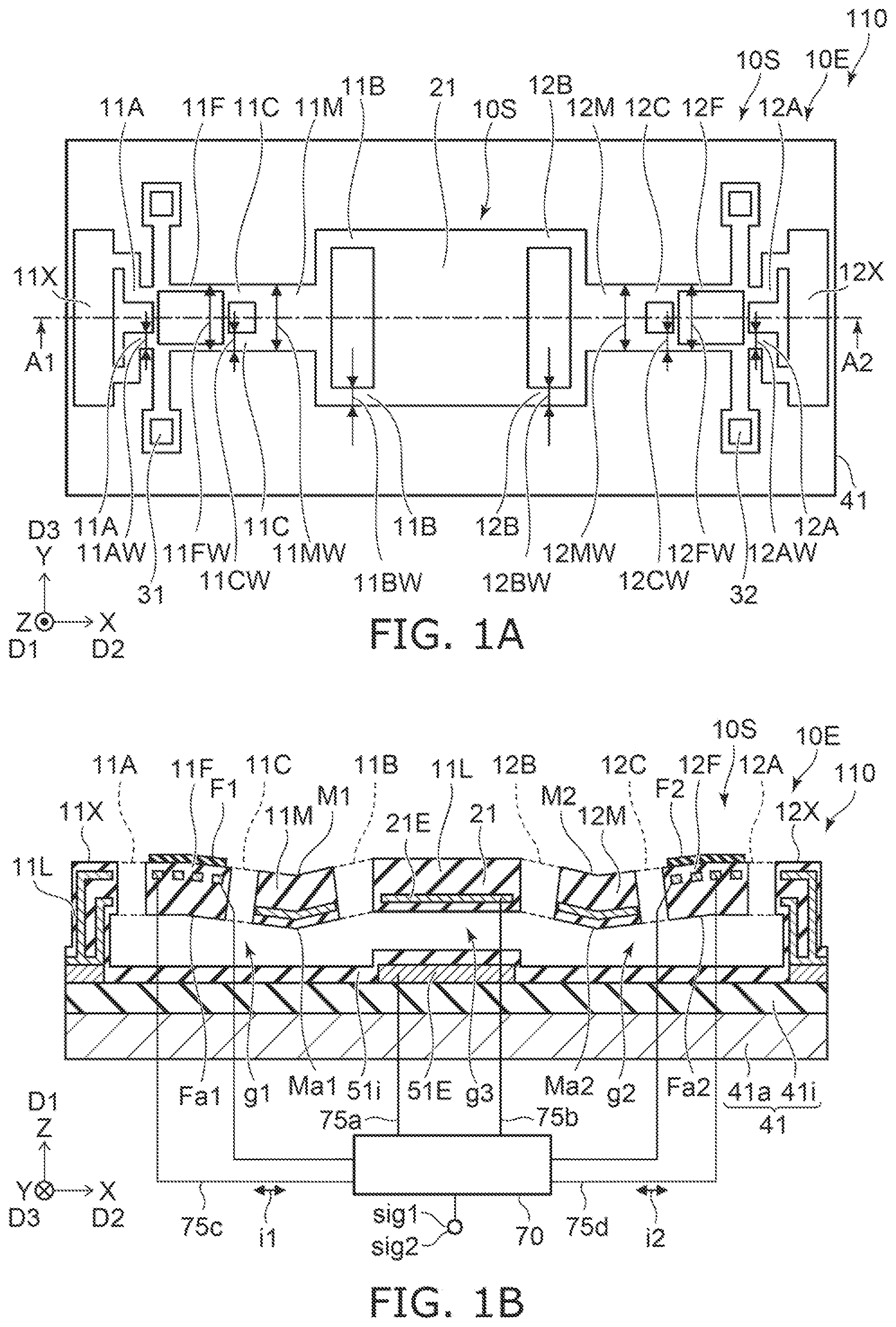
A and 1 B are schematic views illustrating a sensor according to the first embodiment. A is a plan view. B is a cross-sectional view taken along the line A 1 -A 2 of A .
As shown in A and 1 B , a sensor 110 according to the embodiment includes a sensor element 10 E. The sensor element 10 E includes a first base body 41 , a first fixed electrode 51 E, and a first structure body 10 S. The first fixed electrode 51 E is fixed to the first base body 41 .
As shown in B , in this example, the first base body 41 includes a substrate 41 a and an insulating layer 41 i . The substrate 41 a may include, for example, a semiconductor substrate (for example, a silicon substrate). The insulating layer 41 i is provided between the substrate 41 a and the first fixed electrode 51 E. In this example, an insulating layer 51 i is provided on the first fixed electrode 51 E.
The first structure body 10 S includes a first fixed portion 11 X, a first deformable portion 11 F, a first intermediate portion 11 M, and a first movable portion 21 . The first fixed portion 11 X is fixed to the first base body 41 . The first deformable portion 11 F is supported by the first fixed portion 11 X. The first intermediate portion 11 M is supported by the first deformable portion 11 F. The first movable portion 21 is supported by the first intermediate portion 11 M. The first movable portion 21 includes a first movable electrode 21 E. The first movable electrode 21 E faces the first fixed electrode 51 E.
A first gap g 1 is provided between the first base body 41 and the first deformable portion 11 F, and between the first base body 41 and the first intermediate portion 11 M. A gap (third gap g 3 ) is provided between the first fixed electrode 51 E and the first movable electrode 21 E.
In this example, the first structure body 10 S includes a first connection portion 11 C, a first movable connection portion 11 B, and a first fixed connection portion 11 A. The first connection portion 11 C connects the first deformable portion 11 F and the first intermediate portion 11 M. The first movable connection portion 11 B connects the first intermediate portion 11 M and the first movable portion 21 . The first fixed connection portion 11 A connects the first fixed portion 11 X and the first deformable portion 11 F.
The first movable portion 21 may include an insulating member 11 L. The insulating member 11 L is provided around the first movable electrode 21 E, for example.
For example, the first fixed electrode 51 E is provided on the first base body 41 . The first movable portion 21 is provided above the first fixed electrode 51 E.
As shown in B , the first deformable portion 11 F includes a first deformed facing surface Fa 1 and a first deformable surface F 1 . The first deformed facing surface Fa 1 faces the first base body 41 . The first deformed facing surface Fa 1 is between the first base body 41 and the first deformable surface F 1 in a first direction D 1 . The first direction D 1 is a direction from the first base body 41 to the first movable portion 21 . The first deformable surface F 1 is a surface opposite to the first deformed facing surface Fa 1 . The first deformed facing surface Fa 1 is, for example, a lower surface. The first deformable surface F 1 is, for example, an upper surface.
The first intermediate portion 11 M includes a first intermediate facing surface Ma 1 and a first intermediate surface M 1 . The first intermediate facing surface Ma 1 faces the first base body 41 . The first intermediate facing surface Ma 1 is between the first base body 41 and the first intermediate surface M 1 in the first direction D 1 . The first intermediate facing surface Ma 1 is, for example, a lower surface. The first intermediate surface M 1 is, for example, an upper surface.
The first direction D 1 is defined as a Z-axis direction. One direction perpendicular to the Z-axis direction is defined as an X-axis direction. A direction perpendicular to the Z-axis direction and the X-axis direction is defined as a Y-axis direction. The first direction D 1 is, for example, a height direction.
The first deformable surface F 1 can be deformed according to a gas included in a space around the first structure body 10 S. For example, the gas includes a substance to be detected (for example, hydrogen). For example, a shape of the first deformable portion 11 F changes according to a concentration of the substance to be detected.
For example, the first deformable portion 11 F includes a first detection layer 11 S. The first detection layer 11 S adsorbs (or absorbs) the substance to be detected. With adsorption (or absorption), for example, the first detection layer 11 S is deformed (for example, expanded). Along with this, the first deformable portion 11 F is deformed, and the first deformable surface F 1 is curved. On the other hand, the first intermediate portion 11 M does not deform even if the concentration of the detection target changes.
On the other hand, the first deformable portion 11 F and the first intermediate portion 11 M are deformed in response to a change in temperature (for example, the temperature of the first structure body 10 S). The directions of these deformations are different between the first deformable portion 11 F and the first intermediate portion 11 M. For example, as the temperature rises, the first deformable surface F 1 and the first intermediate surface M 1 are deformed in opposite directions to each other. For example, as the temperature rises, the first deformable surface F 1 is deformed into one of a concave shape or a convex shape. The first intermediate surface M 1 is deformed into the other of the concave shape and the convex shape.
B illustrates a high temperature state. In this example, in the high temperature state, the first deformable surface F 1 is deformed in the concave shape, and the first intermediate surface M 1 is deformed in the convex shape. As will be described later, in the high temperature state, the first deformable surface F 1 may be deformed in the convex shape, and the first intermediate surface M 1 may be deformed in the concave shape. As a result, more stable characteristics can be obtained.
A and 2 B are schematic cross-sectional views illustrating the sensor according to the first embodiment.
A illustrates a low temperature state. The temperature in the low temperature state illustrated in A is lower than the temperature in the high temperature state illustrated in B . The temperature in the low temperature state is, for example, about 25° C. (not lower than 20° C. and not higher than 30° C.). The temperature in the high temperature state is, for example, not lower than 50° C. The temperature in the high temperature state may be, for example, not higher than 70° C.
As shown in A , the first deformable surface F 1 of the first deformable portion 11 F is substantially flat in the low temperature state. In the low temperature state, the first intermediate surface M 1 of the first intermediate portion 11 M is substantially flat.
On the other hand, in the high temperature state illustrated in B , the first deformable surface F 1 of the first deformable portion 11 F and the first intermediate surface M 1 of the first intermediate portion 11 M are curved. The direction of the curve is opposite to each other between the first deformable surface F 1 and the first intermediate surface M 1 .
Such a structure is obtained, for example, by making the structure of the first deformable portion 11 F asymmetric in the vertical direction and making the structure of the first intermediate portion 11 M asymmetric in the vertical direction. For example, thermal expansion with a rise of a temperature deforms the asymmetric structure. This provides the curve in the opposite direction. An example of the asymmetric structure will be described later.
In the following, an example of deformation will be described.
A to 3 C are schematic cross-sectional views illustrating the operation of the sensor according to the first embodiment.
A first state ST 1 shown in A is the low temperature state, and in the first state ST 1 , the gas does not include the substance to be detected. In the first state ST 1 , the first deformable surface F 1 and the first intermediate surface M 1 are substantially flat. At this time, a distance between the first fixed electrode 51 E and the first movable electrode 21 E is a distance z 1 .
A second state ST 2 shown in B is the low temperature state, and in the second state ST 2 , the gas includes the substance to be detected. In this case, the first deformable portion 11 F is deformed according to the substance to be detected. When a concentration of the substance to be detected is high, the first deformable surface F 1 is deformed convexly. An end of the first deformable surface F 1 on a side of the first intermediate portion 11 M is displaced in a direction of the arrow AR 1 (for example, downward). As a result, a position of the first movable portion 21 in the second state ST 2 in the height direction changes from a position of the first movable portion 21 in the first state ST 1 in the height direction. In the second state ST 2 , a distance between the first fixed electrode 51 E and the first movable electrode 21 E is a distance z 2 . The distance z 2 is shorter than the distance z 1 . This difference in distance is detected as a change in capacitance between the first fixed electrode 51 E and the first movable electrode 21 E.
A third state ST 3 shown in C is the high temperature state, and in the third state ST 3 , the gas does not include the substance to be detected. In the third state ST 3 , for example, the first deformable surface F 1 is deformed convexly due to the deformation caused by the thermal expansion. An end of the first deformable surface F 1 on a side of the first intermediate portion 11 M is displaced in the direction of the arrow AR 1 (for example, downward). On the other hand, with the deformation caused by thermal expansion, for example, the first intermediate surface M 1 is deformed in the concave shape. An end of the first intermediate surface M 1 on a side of the first movable portion 21 is displaced in a direction of the arrow AR 2 (for example, upward). As a result, a position of the first movable portion 21 in the third state ST 3 in the height direction does not substantially change from the position of the first movable portion 21 in the first state ST 1 in the height direction. For example, a distance between the first fixed electrode 51 E and the first movable electrode 21 E in the third state ST 3 is the distance z 1 .
As described above, in the sensor 110 according to the embodiment, the change in the distance between the first fixed electrode 51 E and the first movable electrode 21 E due to the change in temperature can be suppressed. In the embodiment, the influence of temperature can be suppressed and the substance to be detected included in the gas can be detected with high accuracy.
A to 4 C are schematic cross-sectional views illustrating the operation of a sensor according to a reference example.
These figures illustrate the operation of a sensor 119 of the reference example. The sensor 119 is not provided with the first intermediate portion 11 M that deforms in the opposite direction to the first deformable portion 11 F.
In the first state ST 1 shown in A , the first deformable surface F 1 and the first intermediate surface M 1 are substantially flat. At this time, the distance between the first fixed electrode 51 E and the first movable electrode 21 E is the distance z 1 .
In the second state ST 2 shown in B , the first deformable portion 11 F is deformed in a convex shape according to the substance to be detected. The distance between the first fixed electrode 51 E and the first movable electrode 21 E in the second state ST 2 is the distance z 2 . The distance z 2 is shorter than the distance z 1 . This difference in distance is detected as a change in capacitance between the first fixed electrode 51 E and the first movable electrode 21 E.
In the third state ST 3 shown in C , for example, the first deformable surface F 1 is deformed convexly with the deformation caused by the thermal expansion. As a result, a position of the first movable portion 21 in the third state ST 3 in the height direction changes from the position of the first movable portion 21 in the first state ST 1 in the height direction. For example, the distance between the first fixed electrode 51 E and the first movable electrode 21 E in the third state ST 3 is the distance z 2 .
As described above, in the sensor 119 of the reference example, the first intermediate portion 11 M that deforms in the opposite direction to the first deformable portion 11 F is not provided. In such a sensor 119 , the distance between the first fixed electrode 51 E and the first movable electrode 21 E is affected by the temperature in addition to the concentration of the substance to be detected. Therefore, there is a limit to the improvement of accuracy in the detection of the substance to be detected.
On the other hand, in the embodiment, the influence of temperature can be suppressed. According to the embodiment, it is possible to provide a sensor whose characteristics can be improved.
As shown in A and 2 B , the first deformable portion 11 F includes a first resistance layer 11 R and the first detection layer 11 S. The first detection layer 11 S can be deformed depending on the gas. The first detection layer 11 S is deformed, for example, depending on the concentration of the substance to be detected contained in the gas. At least a part of the first detection layer 11 S may overlap the first resistance layer 11 R in the first direction D 1 . As shown in B , the insulating member 11 L may be provided around the first resistance layer 11 R. For example, the first detection layer 11 S may be provided on the surface of the insulating member 11 L. The first resistance layer 11 R is, for example, a heater.
The insulating member 11 L may include, for example, at least one selected from the group consisting of oxygen and nitrogen, and silicon.
As shown in B , the first intermediate portion 11 M may include a first intermediate conductive layer 11 ML. The insulating member 11 L may be provided around the first intermediate conductive layer 11 ML. A distance along the first direction D 1 between the first intermediate conductive layer 11 ML and the first intermediate facing surface Ma 1 is defined as a first distance d 1 . A distance along the first direction D 1 between the first intermediate conductive layer 11 ML and the first intermediate surface M 1 is defined as a second distance d 2 . In the example shown in B , the first distance d 1 is shorter than the second distance d 2 .
On the other hand, a distance along the first direction D 1 between the first resistance layer 11 R and the first deformed facing surface Fa 1 is defined as a third distance d 3 . A distance along the first direction D 1 between the first resistance layer 11 R and the first deformable surface F 1 is defined as a fourth distance d 4 . In the example shown in B , the third distance d 3 is longer than the fourth distance d 4 .
In this way, a stacked structure of the layers is reversed between the first intermediate portion 11 M and the first deformable portion 11 F. As a result, the deformation in the opposite direction is obtained with respect to the change in temperature.
As will be described later, in the embodiment, the first distance d 1 may be longer than the second distance d 2 , and the third distance d 3 may be shorter than the fourth distance d 4 .
As shown in A , a first connection direction (in this example, the second direction D 2 and the X-axis direction) from the first deformable portion 11 F to the first intermediate portion 11 M crosses the first direction D 1 . A width 11 CW along a first connection crossing direction of at least a part of the first connection portion 11 C is narrower than a width 11 MW along the first connection crossing direction of the first intermediate portion 11 M. The first connection crossing direction crosses a plane including the first direction D 1 and the first connection direction. In this example, the first connection crossing direction is a third direction D 3 , for example, the Y-axis direction.
As shown in A , a first movable connection direction (in this example, the second direction D 2 and the X-axis direction) from the first intermediate portion 11 M to the first movable portion 21 crosses the first direction D 1 . A width 11 BW along a first movable connection crossing direction of at least a part of the first movable connection portion 11 B is narrower than a width 11 MW along the first movable connection crossing direction of the first intermediate portion 11 M. The first movable connection crossing direction crosses a plane including the first direction D 1 and the first movable connection direction. In this example, the first movable connection crossing direction is the third direction D 3 , for example, the Y-axis direction.
As shown in A , a first fixed connection direction (in this example, the second direction D 2 and the X-axis direction) from the first fixed portion 11 X to the first deformable portion 11 F crosses the first direction D 1 . A width 11 AW along a first fixed connection crossing direction of at least a part of the first fixed connection portion 11 A is narrower than a width 11 FW along the first fixed connection crossing direction of the first deformable portion 11 F. The first fixed connection crossing direction crosses a plane including the first direction D 1 and the first fixed connection direction. In this example, the first fixed connection crossing direction is the third direction D 3 , for example, the Y-axis direction.
As shown in A and 1 B , the first structure body 10 S may include a second fixed portion 12 X fixed to the first base body 41 and a second deformable portion 12 F supported by the second fixed portion 12 X, and a second intermediate portion 12 M supported by the second deformable portion 12 F. The first movable portion 21 is supported by the first intermediate portion 11 M and the second intermediate portion 12 M. A second gap g 2 is provided between the first base body 41 and the second deformable portion 12 F, and between the first base body 41 and the second intermediate portion 12 M.
The second deformable portion 12 F includes a second deformed facing surface Fa 2 facing the first base body 41 and a second deformable surface F 2 . The second deformed facing surface Fa 2 is between the first base body 41 and the second deformable surface F 2 in the first direction D 1 . The second intermediate portion 12 M includes a second intermediate facing surface Ma 2 facing the first base body 41 and a second intermediate surface M 2 . The second intermediate facing surface Ma 2 is between the first base body 41 and the second intermediate surface M 2 in the first direction D 1 .
The second deformable surface F 2 can be deformed according to the gas included in the space. For example, as the temperature rises, the second deformable surface F 2 is deformed to one of the concave shape or the convex shape, and the second intermediate surface M 2 is deformed into the other of the concave shape or the convex shape.
The first movable portion 21 is between the first intermediate portion 11 M and the second intermediate portion 12 M. By providing the second fixed portion 12 X, the second deformable portion 12 F, and the second intermediate portion 12 M in the first structure body 10 S, the distance between the first fixed electrode 51 E and the first movable electrode 21 E becomes more stable.
In this example, the first structure body 10 S includes a second connection portion 12 C, a second movable connection portion 12 B, and a second fixed connection portion 12 A. The second connection portion 12 C connects the second deformable portion 12 F and the second intermediate portion 12 M. The second movable connection portion 12 B connects the second intermediate portion 12 M and the first movable portion 21 . The second fixed connection portion 12 A connects the second fixed portion 12 X and the second deformable portion 12 F.
As shown in A , the first connection direction from the second deformable portion 12 F to the second intermediate portion 12 M (in this example, along the second direction D 2 and along the X-axis direction) crosses the first direction D 1 . A width 12 CW along a second connection crossing direction of at least a part of the second connection portion 12 C is narrower than a width 12 MW along the second connection crossing direction of the second intermediate portion 12 M. The second connection crossing direction crosses a plane including the first direction D 1 and the second connection direction. In this example, the second connection crossing direction is the third direction D 3 , for example, the Y-axis direction.
As shown in A , the first movable connection direction (in this example, along the second direction D 2 and along the X-axis direction) from the second intermediate portion 12 M to the first movable portion 21 crosses the first direction D 1 . A width 12 BW along a second movable connection crossing direction of at least a part of the second movable connection portion 12 B is narrower than a width 12 MW along the second movable connection crossing direction of the second intermediate portion 12 M. The second movable connection crossing direction crosses a plane including the first direction D 1 and the second movable connection direction. In this example, the second movable connection crossing direction is along the third direction D 3 , for example, along the Y-axis direction.
As shown in A , a second fixed connection direction (in this example, along the second direction D 2 and along the X-axis direction) from the second fixed portion 12 X to the second deformable portion 12 F crosses the first direction D 1 . A width 12 AW along the second fixed connection crossing direction of at least a part of the second fixed connection portion 12 A is narrower than a width 12 FW along a second fixed connection crossing direction of the second deformable portion 12 F. The first fixed connection crossing direction crosses a plane including the first direction D 1 and the second fixed connection direction. In this example, the second fixed connection crossing direction is the third direction D 3 , for example, the Y-axis direction.
In this example, there is a second deformable portion 12 F between the second fixed portion 12 X and the first movable portion 21 . There is the second intermediate portion 12 M between the second deformable portion 12 F and the first movable portion 21 .
As shown in A , for example, the second deformable portion 12 F includes a second resistance layer 12 R and a second detection layer 12 S. The second detection layer 12 S can be deformed depending on the gas. The second detection layer 12 S is deformed, for example, depending on the concentration of the substance to be detected contained in the gas. At least a part of the second detection layer 12 S may overlap the second resistance layer 12 R in the first direction D 1 . As shown in A , the insulating member 11 L may be provided around the second resistance layer 12 R. For example, the second detection layer 12 S may be provided on the surface of the insulating member 11 L.
In the sensor 110 , the conductive layer electrically connected to the first movable electrode 21 E may pass through the first fixed portion 11 X and the second fixed portion 12 X. For example, the conductive layer electrically connected to the first resistance layer 11 R may pass through the first fixed portion 11 X and the second fixed portion 12 X. For example, the conductive layer electrically connected to the second resistance layer 12 R may pass through the first fixed portion 11 X and the second fixed portion 12 X.
As shown in A , in this example, the first deformable portion 11 F is supported by the tension provided by an anchor spring 31 . The second deformable portion 12 F is supported by the tension provided by an anchor spring 32 . As a result, a stable support state can be obtained while suppressing heat conduction.
A and 5 B are schematic cross-sectional views illustrating a sensor according to the first embodiment.
As shown in A , in the sensor 111 according to the embodiment, the first deformable surface F 1 is deformed into the concave shape and the first intermediate surface M 1 is changed into the concave shape as the temperature rises. The influence of temperature can also be suppressed in the sensor 111 .
As shown in B , the first distance d 1 is longer than the second distance d 2 , and the third distance d 3 is shorter than the fourth distance d 4 . Such a configuration causes deformation in the sensor 111 . The configuration of the sensor 111 other than the above may be the same as the configuration of the sensor 110 .
is a schematic cross-sectional view illustrating a sensor according to the first embodiment.
As shown in , in a sensor 112 according to the embodiment, the first movable portion 21 includes a conductive layer 21 A in addition to the first movable electrode 21 E. The conductive layer 21 A is stacked with the first movable electrode 21 E. The conductive layer 21 A is, for example, the same layer as the first resistance layer 11 R. The configuration of the sensor 112 other than the above may be the same as the configuration of the sensor 110 .
A to 7 C are schematic cross-sectional views illustrating the operation of a sensor according to the first embodiment.
As shown in A , in a sensor 113 according to the embodiment, the first movable electrode 21 E is substantially the same layer as the first resistance layer 11 R. Except for this, the configuration of the sensor 113 may be the same as that of the sensor 110 .
In this example, as shown in B , in the sensor 113 , the first distance d 1 is shorter than the second distance d 2 . The third distance d 3 is shorter than the fourth distance d 4 . In this case, the first detection layer 11 S is provided on the first deformable surface F 1 .
As shown in C , in a sensor 114 according to the embodiment, the first distance d 1 is longer than the second distance d 2 . The third distance d 3 is longer than the fourth distance d 4 . The first movable electrode 21 E is substantially the same layer as the first resistance layer 11 R. Except for this, the configuration of the sensor 114 may be the same as that of the sensor 110 . In the sensor 114 , the first detection layer 11 S may be provided on, for example, the first deformable surface F 1 .
is a schematic cross-sectional view illustrating a sensor according to the first embodiment.
As shown in , in a sensor 115 according to the embodiment, the first intermediate conductive layer 11 ML of the first intermediate portion 11 M is provided on the first intermediate facing surface Ma 1 . The first detection layer 11 S is provided on the first deformable surface F 1 . Except for this, the configuration of the sensor 115 may be the same as the configuration of the sensor 110 . The reverse curvature is effectively obtained. The first intermediate conductive layer 11 ML may be, for example, a metal layer or the like.
is a schematic plan view illustrating a sensor according to the first embodiment.
As shown in , in a sensor 116 according to the embodiment, a direction from the first fixed portion 11 X to the first deformable portion 11 F is along the second direction (X-axis direction). A direction from the first deformable portion 11 F to the first intermediate portion 11 M is along the third direction D 3 (Y-axis direction). In this way, the direction from the first fixed portion 11 X to the first deformable portion 11 F crosses the direction from the first deformable portion 11 F to the first intermediate portion 11 M. A direction from the first intermediate portion 11 M to the first movable portion 21 is the second direction D 2 (X-axis direction). In this way, the direction from the first intermediate portion 11 M to the first movable portion 21 crosses the direction from the first deformable portion 11 F to the first intermediate portion 11 M. As described above, the arrangement of the first fixed portion 11 X, the first deformable portion 11 F, the first intermediate portion 11 M, and the first movable portion 21 can be variously deformed. The configuration of the sensor 116 other than the above may be the same as the configuration of the sensor 110 or the like, for example.
The influence of temperature can also be suppressed in the sensors 111 to 116 . According to the embodiment, it is possible to provide a sensor whose characteristics can be improved.
Second Embodiment
In the second embodiment, the sensor is configured to perform a test mode operation in addition to a detection mode operation. The test mode operation is, for example, a self-diagnosis mode operation. This operation may be performed by, for example, a controller 70 . In the following, an example of the sensor 110 will be described. The following description can be applied to other sensors (sensors 111 to 116 , etc.).
As shown in B , the sensor 110 may include the controller 70 . The controller 70 is electrically connected to the first fixed electrode 51 E and the first movable electrode 21 E. The electrical connection is made, for example, by wirings 75 a and 75 b.
The controller 70 is configured to perform a first mode operation. The controller 70 is configured to output a first signal sig 1 according to the first capacitance between the first fixed electrode 51 E and the first movable electrode 21 E in the first mode operation. The first capacitance changes depending on the gas included in the space around the first structure body 10 S. The first capacitance changes, for example, depending on the concentration of the substance to be detected included in the gas. The first mode operation is the detection mode operation.
The controller 70 may be configured to perform a second mode operation. In the second mode operation, the controller 70 detects the first capacitance while supplying a first current i 1 to the first resistance layer 11 R (first detection). In the second mode operation, the controller 70 detects the first capacitance without supplying the first current i 1 to the first resistance layer 11 R (second detection). In the second detection, a current smaller than the first current i 1 may be supplied. The controller 70 is configured to output a second signal sig 2 based on a difference between the first result in which the first capacitance is detected in the first detection and the second result in which the first capacitance is detected in the second detection. The second signal sig 2 includes a signal (information) regarding the presence or absence of abnormality in the sensor element 10 E.
In the embodiment, the controller 70 may be configured to output the second signal sig 2 regarding to the presence/absence of abnormality of the sensor element 10 E based on the result of detecting the first capacitance while supplying the first current i 1 to the first resistance layer 11 R in the second mode operation.
In the second mode operation, the first current i 1 may be supplied via, for example, a wiring 75 c . In the second mode operation, the controller 70 may supply a second current i 2 to the second resistance layer 12 R (heater). The second current i 2 may be supplied, for example, via the wiring 75 d (see B ).
is a graph illustrating the operation of a sensor according to a second embodiment.
The horizontal axis of is a current value Ia 1 of the first current i 1 and the second current i 2 . The horizontal axis may be a voltage value Val corresponding to the current value Ia 1 . The vertical axis is the first capacitance C 1 .
For example, when the first current i 1 (and the second current i 2 ) is supplied, the temperature of the first deformable portion 11 F (and the second deformable portion 12 F) rises due to Joule heat, and the first deformable portion 11 F (and the second deformable portion 12 F) is deformed. At this time, the temperature of the first intermediate portion 11 M (and the second intermediate portion 12 M) is maintained lower than the temperature of the first deformable portion 11 F (and the second deformable portion 12 F). Due to the deformation of the deformable portion, the distance between the first fixed electrode 51 E and the first movable electrode 21 E changes, and the first capacitance C 1 changes.
In this example, as the current value Ia 1 increases, the first capacitance C 1 increases. As the voltage value Val increases, the first capacitance C 1 increases. Information (design data) regarding the relationship between the current value Ia 1 (or voltage value Val) and the first capacitance C 1 may be acquired in advance. By comparing this design data with the measurement results, it is possible to detect anomalies.
is a schematic view illustrating the operation of the sensor according to the second embodiment.
The horizontal axis of is time tm 0 . The vertical axis in the lower figure of is an applied voltage VR to the resistance layer supplied from the controller 70 . The applied voltage VR may be the magnitude of the supplied current.
In the first mode operation MO 1 , the controller 70 performs measurement MC 1 of the first capacitance C 1 . The measurement MC 1 may be repeated. In each of the multiple measurements MC 1 , a voltage Vm 1 (current Im 1 ) may be supplied to the resistance layer from the controller 70 . Alternatively, the voltage Vm 1 (current Im 1 ) may be supplied to the resistance layer from the controller 70 before or after each of the multiple measurements MC 1 . As a result, the temperature of the detection layer (first detection layer 11 S and second detection layer 12 S) rises, and the substance adsorbed on the detection layer can be separated. In the multiple measurements MC 1 , the characteristics of the detection layer are initialized.
In the second mode operation MO 2 , a first voltage Vt 1 (or first current It 1 ) is supplied to the resistance layer (first resistance layer 11 R and second resistance layer 12 R) by the controller 70 . In this state, the measurement MC 1 of the first capacitance C 1 is performed. This measurement MC 1 corresponds to the first detection.
In this example, in the second mode operation MO 2 , a second voltage Vt 2 (or second current It 2 ) is supplied to the resistance layer (first resistance layer 11 R and second resistance layer 12 R) by the controller 70 . In this state, the measurement MC 1 of the first capacitance C 1 is performed. This measurement MC 1 corresponds to the second detection. In the second detection, the second voltage Vt 2 (or second current It 2 ) may be substantially zero. The controller 70 outputs the second signal sig 2 based on the difference between the result of the first detection and the result of the first detection.
The controller 70 may repeatedly performs a set MZ 1 of the first mode operation MO 1 and the second mode operation MO 2 .
is a schematic view illustrating the operation of the sensor according to the second embodiment.
The horizontal axis of is time tm 0 . The vertical axis of is a difference ΔCm between the value detected by the first detection and the value detected by the second detection. As shown in , the detection results of each of the multiple sets MZ 1 are plotted. For example, a reference value RG 0 is provided for the difference ΔCm. If the measured value of the difference ΔCm is within the reference value RG 0 , it is determined that there is no abnormality. When the measured value of the difference ΔCm deviates from the reference value RG 0 , it is determined that there is an abnormality. In this case, the second signal sig 2 of “abnormality” is output from the controller 70 in the sensor element 10 E.
is a schematic view illustrating the operation of the sensor according to the second embodiment.
Also in the example of , in the first mode operation MO 1 , the measurement MC 1 of the first capacitance C 1 is performed by the controller 70 . The measurement MC 1 may be repeated. In each of the multiple measurements MC 1 , the voltage Vm 1 (current Im 1 ) may be supplied to the resistance layer from the controller 70 . Alternatively, the voltage Vm 1 (current Im 1 ) may be supplied to the resistance layer from the controller 70 before or after each of the multiple measurements MC 1 .
In the second mode operation MO 2 , the first voltage Vt 1 (or first current It 1 ) is supplied to the resistance layer (first resistance layer 11 R and second resistance layer 12 R) by the controller 70 . In this state, the measurement MC 1 of the first capacitance C 1 is performed. In this example, the controller 70 outputs a second signal sig 2 regarding the presence or absence of an abnormality in the sensor element 10 E based on the detection result. The controller 70 may repeatedly perform the set MZ 1 of the first mode operation MO 1 and the second mode operation MO 2 .
is a schematic view illustrating the operation of the sensor according to the second embodiment.
The horizontal axis of is time tm 0 . The vertical axis of is the measured value Cm by the measurement MC 1 of the first capacitance C 1 . As shown in , the detection results of each of the multiple sets MZ 1 are plotted. For example, the reference value RG 0 is provided for the measured value Cm. If the measured value Cm is within the reference value RG 0 , it is determined that there is no abnormality. When the measured value Cm deviates from the reference value RG 0 , it is determined that there is an abnormality. In this case, the second signal sig 2 of “abnormality” is output from the controller 70 in the sensor element 10 E.
is a schematic view illustrating the operation of the sensor according to the second embodiment.
shows an example of processing that is configured to be performed by the controller 70 .
For example, a resistance Rh of the resistance layer (first resistance layer 11 R and second resistance layer 12 R) is compared with a reference value Rth 1 (step S 11 ). When the resistance Rh is lower than the reference value Rth 1 , it is determined as an error ER 1 (step S 21 ). The error ER 1 corresponds to “circuit short”.
If the resistance Rh is not lower than the reference value Rth 1 , the process proceeds to step S 12 . In step S 12 , the resistance Rh is compared with a reference value Rth 2 . When the resistance Rh is higher than the reference value Rth 2 , it is determined as an error ER 2 (step S 22 ). The error ER 2 corresponds to “disconnection”.
If the resistance Rh is not higher than the reference value Rth 2 , the process proceeds to step S 13 . In step S 13 , a ratio dC/dTh is compared with a reference value V 01 . The ratio dC/dTh is a ratio of the change (dC) of the first capacitance C 1 to the change of temperature (dTh). This change in temperature (dTh) is a change in temperature due to application of voltage (or supply of current) to the heaters (first resistance layer 11 R and second resistance layer 12 R). The change in temperature in this case is not a change in the temperature of the environment. When the ratio dC/dTh is lower than the reference value V 01 , it is determined as an error ER 3 (step S 23 ). The error ER 3 corresponds to the “decrease in ratio”. “Decrease in ratio” is one example of anomalies. Instead of comparing the ratio dC/dTh with the reference value V 01 , for example, the difference ΔCm may be compared with the reference value. Instead of comparing the ratio dC/dTh with the reference value V 01 , for example, the measured value Cm may be compared with the reference value.
If the ratio dC/dTh is not lower than the reference value V 01 , the process proceeds to step S 14 . In step S 14 , the ratio dC/dTh is compared with a reference value V 02 . When the ratio dC/dTh is higher than the reference value V 02 , it is determined as an error ER 4 (step S 24 ). The error ER 4 corresponds to the “increase in ratio”. “Increase in ratio” is one example of anomalies.
If the ratio dC/dTh is not higher than the reference value V 02 , the process ends. In this case, it is determined that there is no abnormality.
is a schematic view illustrating a sensor according to the second embodiment.
As shown in , a sensor 117 according to the embodiment includes multiple sensor elements 10 E. For example, the first mode operation MO 1 and the second mode operation MO 2 described above are performed using one of the multiple sensor elements 10 E. For example, in the second mode operation MO 2 , when the second signal sig 2 indicates that there is an abnormality with respect to one of the multiple sensor elements 10 E, the controller 70 is configured to perform the first mode operation MO 1 with respect to another one of the multiple sensor elements 10 E. The first mode operation MO 1 and the second mode operation MO 2 may be repeatedly performed with respect to the other one of the multiple sensor elements 10 E.
By providing the multiple sensor elements 10 E, if an abnormality occurs in one sensor element 10 E, detection can be continuously performed by another sensor element 10 E.
A and 17 B are schematic views illustrating sensors according to the second embodiment.
As shown in A , in a sensor 120 , the controller 70 is provided on the first base body 41 of the sensor element 10 E. The controller 70 may include, for example, a circuit (for example, CMOS: complementary metal oxide semiconductor or the like) formed in a part of the first base body 41 .
As shown in B , a sensor 121 may be provided with the controller 70 separately from the first base body 41 of the sensor element 10 E. The controller 70 may include, for example, a microcomputer or the like.
Third Embodiment
The third embodiment relates to a capacitor device.
A and 18 B are schematic views illustrating a capacitor device according to a third embodiment.
A is a plan view. B is a cross-sectional view taken along the line A 1 -A 2 of A .
As shown in A and 18 B , a capacitor device 210 according to the embodiment includes the sensor element 10 E. The sensor element 10 E includes the first base body 41 , the first fixed electrode 51 E, and the first structure body 10 S. The first fixed electrode 51 E is fixed to the first base body 41 .
The first structure body 10 S includes the first fixed portion 11 X fixed to the first base body 41 , the first deformable portion 11 F supported by the first fixed portion 11 X, the first intermediate portion supported by the first deformable portion 11 F, and the first movable portion 21 supported by the first intermediate portion 11 M. The first deformable portion 11 F includes the first resistance layer 11 R. The first movable portion 21 includes the first movable electrode 21 E facing the first fixed electrode 51 E.
The first gap g 1 is provided between the first base body 41 and the first deformable portion 11 F, and between the first base body 41 and the first intermediate portion 11 M. The third gap g 3 is provided between the first fixed electrode 51 E and the first movable electrode 21 E.
The first deformable portion 11 F includes a first deformed facing surface Fa 1 facing the first base body 41 and a first deformable surface F 1 . The first deformed facing surface Fa 1 is between the first base body 41 and the first deformable surface F 1 in the first direction D 1 from the first base body 41 to the first movable portion 21 .
The first intermediate portion 11 M includes the first intermediate facing surface Ma 1 facing the first base body 41 and the first intermediate surface M 1 . The first intermediate facing surface Ma 1 is between the first base body 41 and the first intermediate surface M 1 in the first direction D 1 .
As the temperature rises, the first deformable surface F 1 is deformed into one of the concave shape or the convex shape, and the first intermediate surface M 1 is deformed into the other of the concave shape and the convex shape.
The controller 70 is configured to change the first capacitance C 1 between the first fixed electrode 51 E and the first movable electrode 21 E by supplying a current to the first resistance layer 11 R.
For example, terminals 76 a and 76 b may be provided. The terminal 76 a is electrically connected to the first fixed electrode 51 E by the wiring 75 a . The terminal 76 b is electrically connected to the first movable electrode 21 E by the wiring 75 b . The first capacitance C 1 is generated between these terminals. The first deformable portion 11 F is deformed by the current supplied to the first resistance layer 11 R, and the distance between the first fixed electrode 51 E and the first movable electrode 21 E changes. As a result, the first capacitance C 1 is changed.
In the embodiment, the above-mentioned first intermediate portion 11 M is provided. As a result, the influence of changes in ambient temperature can be suppressed. The first capacitance C 1 can be controlled with high accuracy.
The sensor configuration described with respect to the first embodiment may be applied to the capacitor device according to the third embodiment.
The embodiments include the following configurations (e.g., technical proposals).
Configuration 1
A sensor, comprising:
a sensor element including
•
• a first base body, • a first fixed electrode fixed to the first base body, and • a first structure body,
the first structure body including
•
• a first fixed portion fixed to the first base body, • a first deformable portion supported by the first fixed portion, • a first intermediate portion supported by the first deformable portion, and • a first movable portion supported by the first intermediate portion, the first movable portion including a first movable electrode facing the first fixed electrode,
a first gap being provided between the first base body and the first deformable portion, and between the first base body and the first intermediate portion,
a third gap being provided between the first fixed electrode and the first movable electrode,
the first deformable portion including a first deformed facing surface facing the first base body, and a first deformable surface, the first deformed facing surface being between the first base body and the first deformable surface in a first direction from the first base body to the first movable portion,
the first intermediate portion including a first intermediate facing surface facing the first base body, and a first intermediate surface, the first intermediate facing surface being between the first base body and the first intermediate surface in the first direction,
the first deformable surface being possible to be deformed depending on a gas included in a space around the first structure body, and
with a rise of a temperature, the first deformable surface deforming into one of a concave shape and a convex shape, and the first intermediate surface deforming into an other of the concave shape and the convex shape.
Configuration 2
The sensor according to Configuration 1, wherein
the first structure body includes a first connection portion connecting the first deformable portion and the first intermediate portion,
a first connection direction from the first deformable portion to the first intermediate portion crosses the first direction,
a width of at least a part of the first connection portion along a first connection crossing direction is narrower than a width of the first intermediate portion along the first connection crossing direction, and
the first connection crossing direction crosses a plane including the first direction and the first connection direction.
Configuration 3
The sensor according to Configuration 1, wherein
the first structure body includes a first movable connection portion connecting the first intermediate portion and the first movable portion,
a first movable connection direction from the first intermediate portion to the first movable portion crosses the first direction,
a width of at least a part of the first movable connection portion along the first movable connection crossing direction is narrower than a width of the first intermediate portion along the first movable connection crossing direction, and
the first movable connection crossing direction crosses a plane including the first direction and the first movable connection direction.
Configuration 4
The sensor according to Configuration 1, wherein
the first structure body includes a first fixed connection portion connecting the first fixed portion and the first deformable portion,
the first fixed connection direction from the first fixed portion to the first deformable portion crosses the first direction,
a width of at least a part of the first fixed connection portion along the first fixed connection crossing direction is narrower than a width of the first deformable portion along the first fixed connection crossing direction, and
the first fixed connection crossing direction crosses a plane including the first direction and the first fixed connection direction.
Configuration 5
The sensor according to Configuration 1, wherein
the first deformable portion is between the first fixed portion and the first movable portion, and
the first intermediate portion is between the first deformable portion and the first movable portion.
Configuration 6
The sensor according to Configuration 1, wherein
a direction from the first fixed portion to the first deformable portion crosses a direction from the first deformable portion to the first intermediate portion, and
a direction from the first intermediate portion to the first movable portion crosses the direction from the first deformable portion to the first intermediate portion.
Configuration 7
The sensor according to Configuration 1, wherein
the first deformable portion includes
•
• a first resistance layer and • a first detection layer,
the first detection layer being possible to be deformed depending on the gas.
Configuration 8
The sensor according to Configuration 7, wherein
at least a part of the first detection layer overlaps the first resistance layer in the first direction.
Configuration 9
The sensor according to Configuration 7, wherein
the first intermediate portion includes a first intermediate conductive layer,
a first distance along the first direction between the first intermediate conductive layer and the first intermediate facing surface is shorter than a second distance along the first direction between the first intermediate conductive layer and the first intermediate surface, a third distance along the first direction between the first resistance layer and the first deformed facing surface is longer than a fourth distance along the first direction between the first resistance layer and the first deformable surface, alternatively the first distance is longer than the second distance, and the third distance is shorter than the fourth distance.
Configuration 10
The sensor according to Configuration 7, wherein
the first intermediate portion includes a first intermediate conductive layer,
a first distance along the first direction between the first intermediate conductive layer and the first intermediate facing surface is longer than a second distance along the first direction between the first intermediate conductive layer and the first intermediate surface, and the first resistance layer is between the first base body and the first detection layer, alternatively
the first distance is shorter than the second distance, and the first detection layer is between the first base body and the first resistance layer.
Configuration 11
The sensor according to Configuration 7, wherein
the first intermediate portion includes a first intermediate conductive layer,
the first intermediate conductive layer is provided on the first intermediate facing surface, and
the first detection layer is provided on the first deformable surface.
Configuration 12
The sensor according to Configuration 7, wherein
the first structure body further includes
•
• a second fixed portion fixed to the first base body, • a first deformable portion supported by the second fixed portion, and • a second intermediate portion supported by the second deformable portion,
the first movable portion is supported by the first intermediate portion and the second intermediate portion,
a second gap is provided between the first base body and the second deformable portion and between the first base body and the second intermediate portion,
the second deformable portion includes a second deformed facing surface facing the first base body, and a second deformable surface, the second deformed facing surface is between the first base body and the second deformable surface in the first direction,
the second intermediate portion includes a second intermediate facing surface facing the first base body, and a second intermediate surface, the second intermediate facing surface is between the first base body and the second intermediate surface in the first direction,
the second deformable surface is possible to be deformed depending on a gas included in the space, and
with the rise of the temperature, the second deformable surface is deformed into the one of the concave shape or the convex shape, the first intermediate surface is deformed into the other of the concave shape or the convex shape.
Configuration 13
The sensor according to Configuration 12, wherein
the first movable portion is between the first intermediate portion and the second intermediate portion.
Configuration 14
The sensor according to Configuration 12, wherein
the first structure body includes a second connection portion connecting the second deformable portion and the second intermediate portion,
a second connection direction from the second deformable portion to the second intermediate portion crosses the first direction,
a width of at least a part of the second connection portion along a second connection crossing direction is narrower than a width of the second intermediate portion along the second connection crossing direction, and
the second connection crossing direction crosses a plane including the first direction and the second connection direction.
Configuration 15
The sensor according to Configuration 7, further comprising:
a controller,
the controller being configured to perform a first mode operation,
the controller being configured to output a first signal corresponding to a first capacitance between the first fixed electrode and the first movable electrode in the first mode operation, and
the first capacitance changing depending on the gas included in the space.
Configuration 16
The sensor according to Configuration 15, wherein
the controller is configured to perform a second mode operation, and
in the second mode operation, the controller is configured to output a second signal regarding presence or absence of abnormality in the sensor element based on a difference between a first result obtained by detecting the first capacitance while supplying a first current to the first resistance layer and a second result obtained by detecting the first capacitance without supplying the first current to the first resistance layer.
Configuration 17
The sensor according to Configuration 15, wherein
the controller is configured to perform a second mode operation, and
in the second mode operation, the controller is configured to output a second signal regarding presence or absence of abnormality in the sensor element based on a result obtained by detecting the first capacitance while supplying a first current to the first resistance layer.
Configuration 18
The sensor according to Configuration 15, wherein
the controller is provided on the first base body.
Configuration 19
The sensor according to Configuration 16, comprising:
a plurality of the sensor elements,
in the second mode operation, when the second signal indicates that there is an abnormality with respect to one of the sensor elements, the controller is configured to perform the first mode operation with respect to another one of the sensor elements.
Configuration 20
A capacitor device, comprising:
a first base body;
a first fixed electrode fixed to the first base body;
a first structure body; and
a controller,
the first structure body including
•
• a first fixed portion fixed to the first base body, • a first deformable portion supported by the first fixed portion, the first deformable portion including a first resistance layer, • a first intermediate portion supported by the first deformable portion, and • a first movable portion supported by the first deformable portion, the first movable portion including a first movable electrode facing the first fixed electrode,
a first gap being provided between the first base body and the first deformable portion and between the first base body and the first intermediate portion,
a third gap being provided between the first fixed electrode and the first movable electrode,
the first deformable portion including a first deformed facing surface facing the first base body, and a first deformable surface, the first deformed facing surface being between the first base body and the first deformable surface in a first direction from the first base body to the first movable portion,
the first intermediate portion including a first intermediate facing surface facing the first base body, and a first intermediate surface,
the first intermediate facing surface being between the first base body and the first intermediate surface in the first direction,
with a rise of a temperature, the first deformable surface being deformed into one of a concave shape or a convex shape, the first intermediate surface being deformed into an other of the concave shape or the convex shape, and
the controller being configured to change a first capacitance between the first fixed electrode and the first movable electrode by supplying a current to the first resistance layer.
According to the embodiments, it is possible to provide a sensor and a capacitor device whose characteristics can be improved.
In the specification, a state of being electrically connected includes not only the case of being directly contacted and connected, but also the case of being connected via another conductive member or the like.
In the specification of the application, “perpendicular” and “parallel” refer to not only strictly perpendicular and strictly parallel but also include, for example, the fluctuation due to manufacturing processes, etc. It is sufficient to be substantially perpendicular and substantially parallel.
Hereinabove, exemplary embodiments of the invention are described with reference to specific examples. However, the embodiments of the invention are not limited to these specific examples. For example, one skilled in the art may similarly practice the invention by appropriately selecting specific configurations of components included in sensors and capacitor devices such as base bodies, structure bodies, supporters, deformable portions, intermediate portion, movable portions, fixed electrodes, controllers, etc., from known art. Such practice is included in the scope of the invention to the extent that similar effects thereto are obtained.
Further, any two or more components of the specific examples may be combined within the extent of technical feasibility and are included in the scope of the invention to the extent that the purport of the invention is included.
Moreover, all sensors, and capacitor devices practicable by an appropriate design modification by one skilled in the art based on the sensors, and the capacitor devices described above as embodiments of the invention also are within the scope of the invention to the extent that the purport of the invention is included.
Various other variations and modifications can be conceived by those skilled in the art within the spirit of the invention, and it is understood that such variations and modifications are also encompassed within the scope of the invention.
While certain embodiments have been described, these embodiments have been presented by way of example only, and are not intended to limit the scope of the inventions. Indeed, the novel embodiments described herein may be embodied in a variety of other forms; furthermore, various omissions, substitutions and changes in the form of the embodiments described herein may be made without departing from the spirit of the inventions. The accompanying claims and their equivalents are intended to cover such forms or modifications as would fall within the scope and spirit of the invention.
Figures (17)
Citations
This patent cites (7)
- US11085836
- US20160363553
- US20190086377
- US20200011827
- US20200080954
- US20220018820
- US2019-56607