Abstract
The disclosure relates to a light board and a spotlight. The light board comprises a circuit board having multiple mounting positions, and lamp beads mounted in the mounting positions, which comprise multiple cool color lamp beads and multiple warm color lamp beads, the cool and warm color lamp beads are configured to form multiple lamp bead rows, which are arranged along a first direction. Each lamp bead row comprises both the cool and warm color lamp beads, a difference between the number of the cool and warm color lamp beads does not exceed 2, a difference between the number of the cool and warm color lamp beads in two adjacent lamp bead rows does not exceed 3, and a total number of cool color lamp beads is equal to that of warm color lamp beads. The technical solution of the disclosure is beneficial to improve lighting effects of lights.
Claims (3)
1. A spotlight comprising a light body and an electric control device, wherein the light body comprises a light board, the light board comprises a circuit board and lamp beads; wherein the circuit board defines mounting positions, the lamp beads are mounted in the mounting positions and comprise cool color lamp beads and warm color lamp beads, the cool color lamp beads and the warm color lamp beads are configured to form lamp bead rows, and the lamp bead rows are arranged along a first direction; wherein each lamp bead row comprises both the cool color lamp beads and the warm color lamp beads, a difference between the number of the cool color lamp beads and the number of the warm color lamp beads does not exceed 2, a difference between a total number of the cool color lamp beads and a total number of the warm color lamp beads in two adjacent lamp bead rows does not exceed 3, and a total number of all the cool color lamp beads on the circuit board is equal to a total number of the warm color lamp beads; the electric control device comprises an outer housing, a battery, and a main control board; wherein the outer housing defines a first mounting chamber, an air cooling passage, and a second mounting chamber; the air cooling passage is located between the first mounting chamber and the second mounting chamber; the first mounting chamber and the air cooling passage are separated by a first partition plate; the second mounting chamber and the air cooling passage are separated by a second partition plate; the outer housing further defines an air inlet and an air outlet communicated with the air cooling passage; the battery is arranged within the first mounting chamber; the main control board is arranged within the second mounting chamber.
Show 2 dependent claims
2. The spotlight according to claim 1 , wherein the electric control device further comprises a first inner housing and a second inner housing that are arranged within the outer housing, the first inner housing encloses the first mounting chamber, the second inner housing encloses the second mounting chamber, and the air cooling passage is located between the first inner housing and the second inner housing, and wherein a housing plate of the first inner housing adjacent to the air cooling passage forms the first partition plate, and a housing plate of the second inner housing adjacent to the air cooling passage forms the second partition plate.
3. The spotlight according to claim 2 , wherein a first connecting plate is protruded from the first partition plate towards the second partition plate, a second connecting plate is protruded from the second partition plate towards the first partition plate, and the first connecting plate is connected with the second connecting plate.
Full Description
Show full text →
TECHNICAL FIELD
The present disclosure relates to a technical field of spotlights, and in particular to a light board and a spotlight.
RELATED ART
With the improvement of people's living standards, lights are no longer just illumination tools, they are widely used into all walks of life. For example, lights are used as supplementary lighting to improve photographic effects in shooting, photography, etc. However, it is difficult to meet the required photographic effect when an existing spotlight is used as a supplementary light, resulting in poor qualities of photos, which cannot meet users' requirements.
SUMMARY
The main purpose of the present disclosure is to provide a light board, which aims to improve the lighting effects emitted by lamps.
In order to achieve the above purpose, a light board is provided by the present disclosure. The light board comprises a circuit board and lamp beads. The circuit board has mounting positions. The lamp beads are mounted in the mounting positions and comprise cool color lamp beads and warm color lamp beads. The cool color lamp beads and the warm color lamp beads are configured to form lamp bead rows, and the lamp bead rows are arranged along a first direction. Each lamp bead row comprises both the cool color lamp beads and the warm color lamp beads. A difference between the number of the cool color lamp beads and that of the warm color lamp beads does not exceed 2. A difference between the total number of the cool color lamp beads and that of the warm color lamp beads in two adjacent lamp bead rows does not exceed 3. A total number of all the cool color lamp beads on the circuit board is equal to that of the warm color lamp beads.
Optionally, the light board has a display area. The display area comprises a first side luminous area, a second side luminous area, and a middle luminous area located between the first side luminous area and the second side luminous area. The first side luminous area comprises lamp bead rows. The number of lamp beads in each lamp bead row gradually increases from an edge to a middle portion of the display area. The second side luminous area comprises lamp bead rows, the number of lamp beads in each lamp bead row gradually increases from an edge to a middle portion of the display area.
Optionally, the number of the cool color lamp beads and the number of the warm color lamp beads in the first side luminous area are equal. The number of the cool color lamp beads and the number of the warm color lamp beads in the second side luminous area are equal. The total number of the lamp beads in the adjacent two lamp bead rows respectively in the first side luminous area and the middle luminous area are equal. The total number of the lamp beads in the adjacent two lamp bead rows respectively in the second side luminous area and the middle luminous area are equal.
Optionally, the middle luminous area comprises a first middle luminous subarea, a second middle luminous subarea, and a central luminous subarea located between the first middle luminous subarea and the second middle luminous subarea. The first middle luminous subarea is arranged adjacent to the first side luminous area, lamp bead rows are arranged within the first middle luminous subarea, and the number of lamp beads in the lamp bead rows gradually increases from near the first side luminous area to near the central luminous subarea. The second middle luminous subarea is arranged adjacent to the second side luminous area, lamp bead rows are arranged within the second middle luminous subarea, and the number of lamp beads in the lamp bead rows gradually increases from near the second side luminous area to near the central luminous subarea.
Optionally, the total numbers of the lamp beads in the adjacent two lamp bead rows respectively in the first middle luminous subarea and the central luminous subarea are equal. The total numbers of the lamp beads in the adjacent two lamp bead rows respectively in the second middle luminous subarea and the central luminous subarea are equal.
Optionally, the central luminous subarea comprises at least three lamp bead rows, and the number of the lamp beads in the lamp bead rows in the central luminous subarea gradually decreases from the middle to the first middle luminous subarea. The number of the lamp beads in the lamp bead rows in the central luminous subarea gradually decreases from the middle to the second middle luminous subarea.
Optionally, the number, the type and arrangement sequence of the lamp beads on a left edge of the first middle luminous subarea is equal to the number, the type and arrangement sequence of the lamp beads on a right edge of the second middle luminous subarea. The number of the lamp beads on a right edge of the first middle luminous subarea is equal to the number of the lamp beads on a left edge of the second middle luminous subarea, and the types of the lamp beads at each corresponding mounting position are different.
Optionally, a difference between the number of cool color lamp beads and the number of warm color lamp beads in each lamp bead row does not exceed 1. The number of the lamp bead rows is an odd row greater than 1, and there is at least one lamp bead row where the number of cool color lamp beads is equal to the number of warm color lamp beads. A difference between the numbers of total color lamp beads in two adjacent lamp bead rows does not exceed 4. The cool color lamp beads and the warm color lamp beads in each lamp bead row are arranged alternately.
Optionally, a color temperature of the cool color lamp beads is greater than or equal to 6000 Kelvin, and is less than or equal to 6500 Kelvin. A color temperature of the warm color lamp beads is greater than or equal to 2600 Kelvin, and is less than or equal to 3000 Kelvin. The mounting positions are arranged in a circular shape.
Optionally, each of the lamp beads comprises a bead body. A bottom of each bead body is provided with a first electrode welding position, a second electrode welding position, and a heat-conducting welding position. There are isolating gaps between any two of the first electrode welding position, the second electrode welding position, and the heat-conducting welding position. The circuit board is provided with the mounting positions for mounting the lamp beads. A positive electrode of the circuit board is electrically connected to the first electrode welding position, and a negative electrode of the circuit board is electrically connected to the second electrode welding position. The light board further comprises a heat-conducting substrate, which is welded to the heat-conducting welding position.
Optionally, the circuit board is provided with mounting holes. The positive and negative electrodes of the circuit board are located on a surface of the circuit board adjacent to the mounting holes. The heat-conducting substrate is welded with the heat-conducting welding position through the mounting holes, and the circuit board is located between the lamp beads and the heat-conducting substrate.
Optionally, the heat-conducting substrate comprises a substrate body and heat-conducting bosses arranged on the substrate body, and the heat-conducting bosses pass through the mounting holes to be welded to the heat-conducting welding positions.
Optionally, a horizontal section of the heat-conducting boss is any one of a circle, an ellipse, a square, and a triangle.
Optionally, an avoiding gap is configured between the adjacent two bosses, and a size of the avoiding gap is 1 mm to 3 mm.
Optionally, a horizontal sectional area of the heat-conducting boss is larger than respective areas of the first electrode welding position, the second electrode welding position, and the heat-conducting welding position.
Optionally, there are gaps between the heat-conducting bosses and the first and second electrode welding positions after the heat-conducting bosses are welded with the heat-conducting welding positions.
Optionally, a thickness of the substrate body is 1 mm to 3 mm, and/or a height of the heat-conducting boss is 0.15 mm to 1 mm.
Optionally, the circuit board is a flexible circuit board, which has a thickness of 0.15 mm to 1 mm.
Optionally, a thickness of the flexible circuit board is equal to the height of the heat-conducting boss.
Optionally, the circuit board has a top layer circuit and a bottom layer circuit, the top layer circuit comprises disconnected top layer circuit units. The bottom layer circuit comprises disconnected bottom layer circuit units. The top layer circuit comprises a positive electrode and a negative electrode, and there are connecting lines arranged in parallel between the positive electrode and the negative electrode. Any one of the connecting lines is used for connecting the lamp beads in the same type in lamp bead rows, and the connecting line is formed by connecting partial top layer circuit units and partial bottom layer circuit units in series.
Optionally, the top layer circuit unit is connected to mounting positions located in different lamp bead rows, and the lamp bead rows connected by the same top layer circuit unit are arranged adjacently in sequence. The bottom layer circuit unit is arranged in strip or block for connecting two different positions of the bottom layer circuit.
Optionally, each connecting line at least comprises two top layer circuit units and two bottom layer circuit units, and the connecting line is formed by alternately connecting the top layer circuit units and the bottom layer circuit units in series.
Optionally, there are positive electrodes and negative electrodes on the top layer circuit, and there are connecting lines arranged in parallel between each positive electrode and the corresponding negative electrode.
Optionally, the positive electrodes comprise a positive electrode A, a positive electrode C, a positive electrode E, and a positive electrode G. The negative electrodes comprise a negative electrode B, a negative electrode D, a negative electrode F, and a negative electrode H. The positive electrode A corresponds to the negative electrode B, the positive electrode C corresponds to the negative electrode D, the positive electrode E corresponds to the negative electrode F, and the positive electrode G corresponds to the negative electrode H.
Optionally, there are a first connecting line, a second connecting line, a third connecting line and a fourth connecting line arranged in parallel between the positive electrode A and the negative electrode B. The first connecting line is formed by: the positive electrode A is connected with a starting point B 1 of a first bottom layer circuit unit B 1 -B 2 through a connecting point A 1 , a connecting point B 2 is connected with a starting point A 3 of a first top layer circuit unit A 3 -A 4 , a connecting point A 4 is connected with a starting point B 3 of a second bottom layer circuit unit B 3 -B 4 , a connecting point B 4 is connected with a starting point A 5 of a second top layer circuit unit A 5 -A 6 , and a connecting point A 6 is connected with the negative electrode B. The second connecting line is formed by: the positive electrode A is connected with the starting point B 1 of the first bottom layer circuit unit B 1 -B 2 through the connecting point A 1 , the connecting point B 2 is connected with a starting point A 8 of a third top layer circuit unit A 8 -A 9 , a connecting point A 9 is connected with a starting point B 5 of a third bottom layer circuit unit B 5 -B 6 , a connecting point B 6 is connected with a starting point A 10 of a fourth top layer circuit unit A 10 -A 11 , and a connecting point A 11 is connected with the negative electrode B. The third connecting line is that: the positive electrode A is connected with the starting point B 1 of the first bottom layer circuit unit B 1 -B 2 through the connecting point A 1 , the connecting point B 2 is connected with a starting point A 12 of a fifth top layer circuit unit A 12 -A 13 , a connecting point A 13 is connected with a starting point B 7 of a fourth bottom layer circuit unit B 7 -B 8 , a connecting point B 8 is connected with a starting point A 14 of a sixth top layer circuit unit A 14 -A 15 , a connecting point A 15 is connected with a starting point B 9 of a fifth bottom layer circuit unit B 9 -B 10 , and a connecting point B 10 is connected with the negative electrode B. The fourth connecting line is formed by: the positive electrode A is connected with the starting point B 1 of the first bottom layer circuit unit B 1 -B 2 through the connecting point A 1 , the connecting point B 2 is connected with a starting point A 16 of a seventh top layer circuit unit A 16 -A 17 , a connecting point A 17 is connected with a starting point B 11 of a sixth bottom layer circuit unit B 11 -B 12 , a connecting point B 12 is connected with a starting point A 18 of an eighth top layer circuit unit A 18 -A 19 , a connecting point A 19 is connected with a starting point B 13 of a seventh bottom layer circuit unit B 13 -B 14 , and a connecting point B 14 is connected with the negative electrode B.
Optionally, there are a fifth connecting line, a sixth connecting line, a seventh connecting line and an eighth connecting line between the positive electrode C and the negative electrode D. The fifth connecting line is formed by: positive electrode C is connected with a starting point D 1 of an eighth bottom layer circuit unit D 1 -D 2 , a connecting point D 2 is connected with a starting point C 2 of a ninth top layer circuit unit C 2 -C 3 , a connecting point C 3 is connected with a starting point D 3 of a ninth bottom layer circuit unit D 3 -D 4 , a connecting point D 4 is connected with a starting point C 4 of a tenth top layer circuit unit C 4 -C 5 , and a connecting point C 5 is connected with the negative electrode D, The sixth connecting line is formed by: the positive electrode C is connected with the starting point D 1 of the eighth bottom layer circuit unit D 1 -D 2 , the connecting point D 2 is connected with a starting point C 6 of an eleventh top layer circuit unit C 6 -C 7 , a connecting point C 7 is connected with a starting point D 5 of a tenth bottom layer circuit unit D 5 -D 6 , a connecting point D 6 is connected with a starting point C 8 of a twelfth top layer circuit unit C 8 -C 9 , and a connecting point C 9 is connected with the negative electrode D. The seventh connecting line is formed by: the positive electrode C is connected with the starting point D 1 of the eighth bottom layer circuit unit D 1 -D 2 , the connecting point D 2 is connected with a starting point C 10 of a thirteenth top layer circuit unit C 10 -C 11 , a connecting point C 11 is connected with a starting point D 7 of an eleventh bottom layer circuit unit D 7 -D 8 , a connecting point D 8 is connected with a starting point C 12 of a fourteenth top layer circuit unit C 12 -C 13 , a connecting point C 13 is connected with a starting point D 9 of a twelfth bottom layer circuit unit D 9 -D 10 , a connecting point D 10 is connected with a starting point C 15 of a fifteenth top layer circuit unit C 15 -C 16 , a connecting point C 16 is connected with a starting point D 11 of a thirteenth bottom layer circuit unit D 11 -D 12 , and a connecting point D 12 is connected with the negative electrode D. The eighth connecting line is that: the positive electrode C is connected with the starting point D 1 of the first bottom layer circuit unit D 1 -D 2 , the connecting point D 2 is connected to the starting point C 1 of a sixteenth top layer circuit unit C 1 -C 17 , a connecting point C 17 is connected to a starting point D 13 of a fourteenth bottom layer circuit unit D 13 -D 14 , a connecting point D 14 is connected with a starting point C 18 of an seventeenth top layer circuit unit C 18 -C 19 , and a connecting point C 19 is connected with the negative electrode D.
Optionally, there are a ninth connecting line, a tenth connecting line, an eleventh connecting line and a twelfth connecting line between the positive electrode E and the negative electrode F. The ninth connecting line is formed by: the positive electrode E is connected with a starting point E 1 of an eighteenth top layer circuit unit E 1 -E 2 , a connecting point E 2 is connected with a starting point E 3 of a nineteenth top layer circuit unit E 3 -E 4 , a connecting point E 4 is connected with a starting point F 1 of a fifteenth bottom layer circuit unit F 1 -F 2 , a connecting point F 2 is connected with a starting point E 5 of a twentieth top layer circuit unit E 5 -E 6 , a connecting point E 6 is connected with a starting point F 3 of a sixteenth bottom layer circuit unit F 3 -F 4 , and a connecting point F 4 is connected with the negative electrode F. The tenth connecting line is formed by: the positive electrode E is connected with a starting point E 7 of a twenty-first top layer circuit unit E 7 -E 8 , a connecting point E 8 is connected with a starting point F 5 of a seventeenth bottom layer circuit unit F 5 -F 6 , a connecting point F 6 is connected with a starting point E 9 of a twenty-second top layer circuit unit E 9 -E 10 , a connecting E 10 is connected with the starting point F 3 of the sixteenth bottom layer circuit unit F 3 -F 4 , and the connecting point F 4 is connected with the negative electrode F. The eleventh connecting line is formed by: the positive electrode E is connected with a starting point E 11 of a twenty-third top layer circuit unit E 11 -E 12 , a connecting point E 12 is connected with a starting point F 7 of an eighteenth bottom layer circuit unit F 7 -F 8 , a connecting point F 8 is connected with a starting point E 13 of a twenty-fourth top layer circuit unit E 13 -E 14 , a connecting point E 14 is connected with the starting point F 3 of the sixteenth bottom layer circuit unit F 3 -F 4 , and the connecting point F 4 is connected with the negative electrode F. The twelfth connecting line is formed by: the positive electrode E is connected with a starting point E 15 of a twenty-fifth top layer unit E 15 -E 16 , a connecting point E 16 is connected with a starting point F 9 of a nineteenth bottom layer circuit unit F 9 -F 10 , a connecting point F 10 is connected with a starting point E 17 of a twenty-sixth top layer circuit unit E 17 -E 18 , a connecting point E 18 is connected to a starting point F 11 of a twentieth bottom layer circuit unit F 11 -F 4 , and the connecting point F 4 is connected with the negative electrode F.
Optionally, there are a thirteenth connecting line, a fourteenth connecting line, a fifteenth connecting line and a sixteenth connecting line between the positive electrode G and the negative electrode H. The thirteenth connecting line is formed by: the positive electrode G is connected with a starting point H 1 of a twenty-first bottom layer circuit unit H 1 -H 2 , a connecting point H 2 is connected with a starting point G 1 of a twenty-seventh top layer circuit unit G 1 -G 2 , a connecting point G 2 is connected with a starting point H 3 of a twenty-second bottom layer circuit unit H 3 -H 4 , a connecting point H 4 is connected with a starting point G 3 of a twenty-eighth top layer circuit unit G 3 -G 4 , a connecting point G 4 is connected with a starting point H 5 of a twenty-third bottom layer circuit unit H 5 -H 6 , and a connecting point H 6 is connected with a starting point G 5 of an electrical connecting block G 5 -H. The fourteenth connecting line is formed by: the positive electrode G is connected with a starting point G 6 of a twenty-ninth top layer circuit unit G 6 -G 7 , a connecting point G 7 is connected with a starting point H 7 of a twenty-fourth bottom layer circuit unit H 7 -H 8 , a connecting point H 8 is connected with a starting point G 8 of a thirtieth top layer circuit unit G 8 -G 9 , a connecting point G 9 is connected with a starting point H 5 of the twenty-third bottom layer circuit unit H 5 -H 6 , and the connecting point H 6 is connected with the starting point G 5 of the electrical connecting block G 5 -H. The fifteenth connecting line is that: the positive electrode G is connected with the starting point H 1 of the twenty-first bottom layer circuit unit H 1 -H 2 , the connecting point H 2 is connected with a starting point G 11 of a thirty-first top layer circuit unit G 11 -G 12 , a connecting point G 12 is connected with a starting point H 9 of a twenty-fifth bottom layer circuit unit H 9 -H 10 , a connecting point H 10 is connected with a starting point G 13 of a thirty-second top layer circuit unit G 13 -G 5 , and the connecting point G 5 is connected with the negative electrode H through the electrical connecting block G 5 -H. The sixteenth connecting line is that: the positive electrode G is connected with the starting point H 1 of the twenty-first bottom layer circuit unit H 1 -H 2 , the connecting point H 2 is connected with a starting point G 10 of an electrical connecting block G 10 -G 11 , a connecting point G 11 is connected with a starting point H 11 of a twenty-sixth bottom layer circuit unit H 11 -H 12 , a connecting point H 12 is connected with a starting point G 15 of a thirty-third top layer circuit unit G 15 -G 16 , a connecting point G 16 is connected with a starting point H 13 of a twenty-seventh bottom layer circuit unit H 13 -H 14 , a connecting point H 14 is connected with a starting point G 17 of a thirty-fourth top layer circuit unit G 17 -G 18 , and a connecting point G 18 is connected with the negative electrode H through an electrical connecting block G 18 -H.
The present disclosure further provides a spotlight, which comprises a light body and an electric control device. The light body comprises a light board. The light board comprises a circuit board having mounting positions and lamp beads mounted within the mounting positions, The lamp beads comprise cool color lamp beads and warm color lamp beads. The cool color lamp beads and the warm color lamp beads are configured to form lamp bead rows. The lamp beads are arranged in a first direction. Each lamp bead row comprises both the cool color lamp beads and the warm color lamp beads. A difference between the number of the cool color lamp beads and that of the warm color lamp beads does not exceed 2. A difference between the number of the cool color lamp beads and that of the warm color lamp beads in two adjacent lamp bead rows does not exceed 3. A total number of the cool color lamp beads is equal to that of the warm color lamp beads.
Optionally, the electric control device comprises an outer housing, a battery arranged within the first mounting chamber, and a main control board arranged within the second mounting chamber. The outer housing comprises a first mounting chamber, an air cooling passage, and a second mounting chamber. The air cooling passage is located between the first mounting chamber and the second mounting chamber. The first mounting chamber and the air cooling passage are separated by a first partition plate. The second mounting chamber and the air cooling passage are separated by a second partition plate. The outer housing is further provided with an air inlet and an air outlet communicating with the air cooling passage.
Optionally, the electric control device of the spotlight further comprises a heat-radiating rotor arranged at the air inlet.
Optionally, the electric control device of the spotlight further comprises a heat-radiating structure.
Optionally, the heat-radiating structure is configured as a heat-radiating rib, and the heat-radiating rib is connected to the second partition plate.
Optionally, the electric control device of the spotlight further comprises a first inner housing and a second inner housing that are arranged within the outer housing. The first inner housing encloses the first mounting chamber, the second inner housing encloses the second mounting chamber, and the air cooling passage is located between the first inner housing and the second inner housing. A housing plate of the first inner housing adjacent to the air cooling passage forms the first partition plate, and a housing plate of the second inner housing adjacent to the air cooling passage forms the second partition plate.
Optionally, a first connecting plate is protruded from the first partition plate towards the second partition plate, a second connecting plate is protruded from the second partition plate towards the first partition plate, and the first connecting plate is connected with the second connecting plate.
Optionally, a middle portion of the first connecting plate is bent to form a buckling groove. An end of the second connecting plate is bent to form a hook groove, and the hook groove and the buckling groove are engaged with each other.
Optionally, an end of the first connecting plate is lapped with the second connecting plate. The first connecting plate is provided with a through-hole. The second connecting plate is provided with a fixing hole corresponding to the through-hole. The through-hole and the fixing hole can be connected through a fastener.
Optionally, a heat-radiating hole is formed at the bottom of the second inner housing, and the heat-radiating hole is communicated with the air cooling passage.
Optionally, the electric control device of the spotlight further comprises an inner top cover. Openings are formed on the top of the first inner housing and the second inner housing, and the inner top cover is covered on the top of the first inner housing and the second inner housing. The inner top cover is provided with an air-passing hole, and the air-passing hole communicates the air inlet with the air cooling passage.
In the technical solution of the present disclosure, the cool color lamp beads and warm color lamp beads are configured to form lamp bead rows, and each lamp bead row comprises both the cool color lamp beads and the warm color lamp beads. A difference between the number of the cool color lamp beads and that of the warm color lamp beads does not exceed 2. A difference between the number of the cool color lamp beads and that of the warm color lamp beads in two adjacent lamp bead rows does not exceed 3. A total number of the cool color lamp beads is equal to that of the warm color lamp beads. When the light board is working, the cool color light emitted by the cool color lamp beads and the warm color light emitted by the warm color lamp beads can be fully mixed, thus the light emitted by the light board is highly close to natural light, which is beneficial to improve the effects of shooting, photography, video, and etc.
BRIEF DESCRIPTION OF THE DRAWINGS
In order to more clearly understand the technical solution hereinafter in embodiments of the present disclosure, a brief description to the drawings used in detailed description of embodiments hereinafter is provided thereof. Apparently, the drawings described below are some embodiments of the present disclosure, for those skilled in the art, other drawings can be obtained according to the drawings below without any creative work.
is a schematic structural view of a light board according an embodiment of the present disclosure;
is a schematic structural view of the light board according another embodiment of the present disclosure;
is partial schematic structural view in ;
is a longitudinal section view of the light board according an embodiment of the present disclosure;
is a partial enlarged view of part A in according to an embodiment;
is a partial enlarged view of part Ain according to another embodiment;
is a schematic structural view of a top layer circuit of the light board according to an embodiment of the present disclosure;
is a schematic structural view of a bottom layer circuit of the light board according to an embodiment of the present disclosure;
is a schematic connection view of a first connecting line of the light board according to an embodiment of the present disclosure;
is a schematic connection view of a second connecting line of the light board according to an embodiment of the present disclosure;
is a schematic connection view of a third connecting line of the light board according to an embodiment of the present disclosure;
is a schematic connection view of a fourth connecting line of the light board according to an embodiment of the present disclosure;
is a schematic connection view of a fifth connecting line of the light board according to an embodiment of the present disclosure;
is a schematic connection view of a sixth connecting line of the light board according to an embodiment of the present disclosure;
is a schematic connection view of a seventh connecting line of the light board according to an embodiment of the present disclosure;
is a schematic connection view of an eighth connecting line of the light board according to an embodiment of the present disclosure;
is a schematic connection view of a ninth connecting line of the light board according to an embodiment of the present disclosure;
is a schematic connection view of a tenth connecting line of the light board according to an embodiment of the present disclosure;
is a schematic connection view of an eleventh connecting line of the light board according to an embodiment of the present disclosure;
is a schematic connection view of a twelfth connecting line of the light board according to an embodiment of the present disclosure;
is a schematic connection view of a thirteenth connecting line of the light board according to an embodiment of the present disclosure;
is a schematic connection view of a fourteenth connecting line of the light board according to an embodiment of the present disclosure;
is a schematic connection view of a fifteenth connecting line of the light board according to an embodiment of the present disclosure;
is a schematic connection view of a sixteenth connecting line of the light board according to an embodiment of the present disclosure;
is a schematic structural view of an electric control device of a spotlight according to an embodiment of the present disclosure;
is a longitudinal section view of the electric control device of the spotlight according to an embodiment of the present disclosure;
is a longitudinal sectional view of the electric control device of the spotlight according to another embodiment of the present disclosure;
is a horizontal section view of the electric control device of the spotlight according to other embodiment of the present disclosure;
is a schematic structural view of a first inner housing and a second inner housing according to an embodiment of the present disclosure;
is a horizontal section view of the first inner housing and the second inner housing according to an embodiment of the present disclosure.
Reference numbers:
Refer- Refer-
ence ence
num- num-
bers Name bers Name
100 circuit board 360 warm color lamp bead
370 cool color lamp bead M1 first side luminous area
M2 second side luminous area M3 middle luminous area
M31 first middle luminous M32 second middle luminous
subarea subarea
M33 central luminous subarea M11 first lamp bead row
M12 second lamp bead row M13 third lamp bead row
M14 fourth lamp bead row M15 fifth lamp bead row
M16 sixth lamp bead row M21 seventh lamp bead row
M22 eighth lamp bead row M23 ninth lamp bead row
M24 tenth lamp bead row M25 eleventh lamp bead row
M26 twelfth lamp bead row M311 thirteenth lamp bead row
M312 fourteenth lamp bead row M313 fifteenth lamp bead row
M321 sixteenth lamp bead row M322 seventeenth lamp bead row
M323 eighteenth lamp bead row M331 nineteenth lamp bead row
M332 twentieth lamp bead row M333 twenty-first lamp bead row
110 mounting hole 200 heat-conducting substrate
210 substrate body 220 heat-conducting boss
300 lamp beads 310 bead body
325 isolating gap 320 first electrode welding
position
330 second electrode welding 350 heat-conducting welding
position position
120 top layer circuit 130 bottom layer circuit
150 mounting positions 160 top layer circuit unit
170 bottom layer circuit unit 181 first connecting line
182 second connecting line 183 third connecting line
184 fourth connecting line 185 fifth connecting line
186 sixth connecting line 187 seventh connecting line
188 eight connecting line 189 ninth connecting line
190 tenth connecting line 191 eleventh connecting line
192 twelfth connecting line 193 thirteenth connecting line
194 fourteenth connecting line 195 fifteenth connecting line
196 sixteenth connecting line 400 outer housing
410 first mounting chamber 420 second mounting chamber
430 air cooling passage 510 first partition plate
520 second partition plate 440 air inlet
450 air outlet 530 battery
550 main control board 560 heat-radiating rotor
570 heat-radiating structure 580 first inner housing
590 second inner housing 610 first connecting plate
620 second connection plate 611 through-hole
621 fixing hole 630 heat-radiating hole
700 inner top cover 710 air-passing hole
The realization, functional features and advantages of the present disclosure will be further described with reference to the accompanying drawings in combination with the embodiments.
Preferred Embodiments of the Present Disclosure
The technical solutions in the embodiments of the present disclosure will be clearly and completely described in conjunction with the accompanying drawings hereafter. Apparently, the described embodiments are part of the embodiments of the present disclosure, rather than all of the embodiments. All other embodiments obtained by those skilled in the art based on the embodiments of the present disclosure without creative efforts shall fall within the protection scope of the present disclosure.
It should be noted that all directional indications (such as up, down, left, right, front, back, etc.) in the embodiments of the present disclosure are merely used for explaining relative relationships, motion, etc. among various components under a certain posture (as shown in the accompanying drawings). If the specific posture changes, the directional indications also change accordingly.
In addition, the descriptions involving “first”, “second”, etc. in the present disclosure are barely for descriptive purposes, but not to be interpreted as indicating or implying relative importance or implicitly indicating the amount of indicated technical features. Thus, a feature defined by “first”, “second” may expressly or implicitly include at least one of that feature. Besides, “and/or” in the full specification includes three solutions, taking A and/or B as an example, including a technical solution A, a technical solution B, and a technical solution that A and B satisfy at the same time. In addition, the technical solutions among various embodiments can be combined mutually, but must be based on the realization by those skilled in the art. When the combination of technical solutions is contradictory or cannot be realized, it should be interpreted that the combination of technical solutions does not exist and not within the protection scope claimed by the present disclosure.
The present disclosure mainly provides a light board, which is mainly used in a spotlight for illumination or used for supplementary lighting during shooting, photography, or video. Apparently, it can also be used to form lighting effects in some specific conditions. In the light board provided by the present disclosure, cool color lamp beads and warm color lamp beads are arranged alternately, and the number of the cool color lamp beads is the same as that of the warm color lamp beads, so that the light board can produce soft and uniform lighting that is close to natural light.
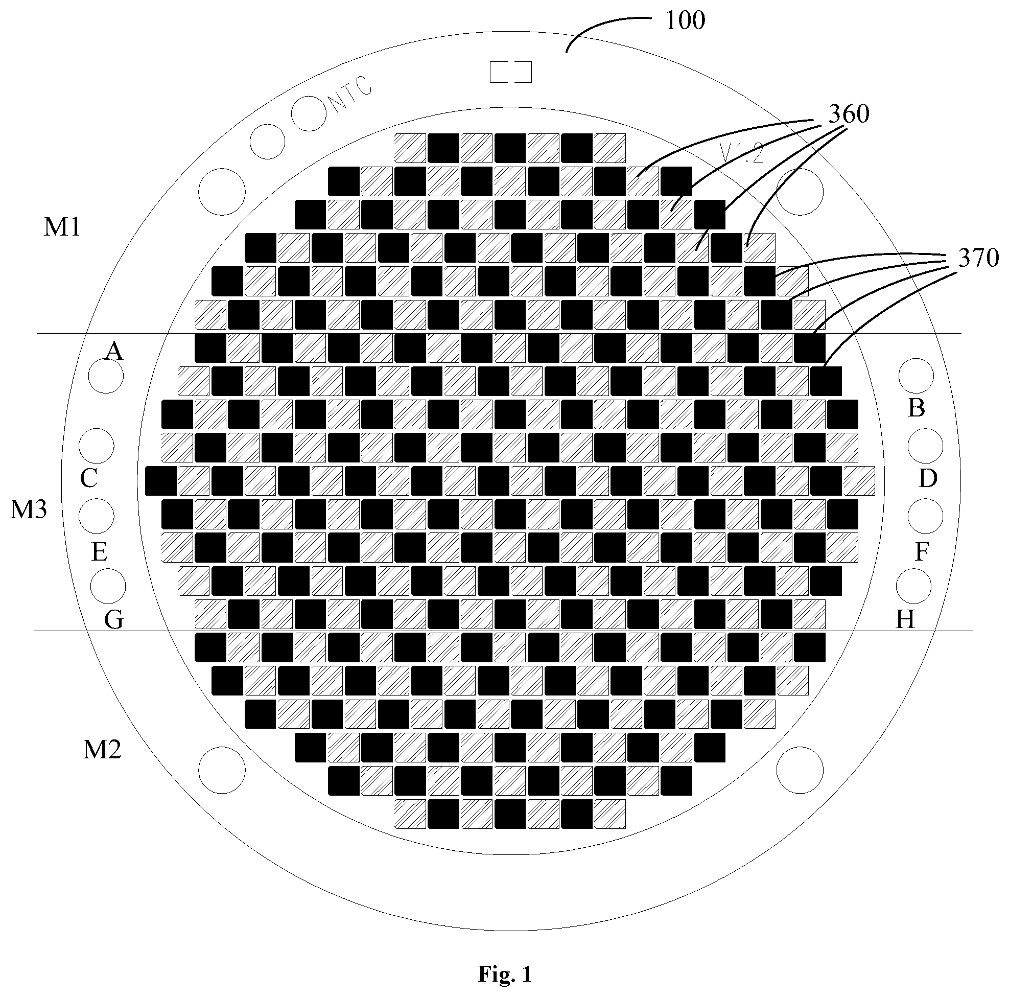
The specific structure of the light board will be mainly described hereafter. Referring to to , in an embodiment of the present disclosure, the light board comprises: a circuit board 100 and lamp beads. The circuit board 100 has a plurality of mounting positions. The amp beads are arranged in the mounting positions and comprise cool color lamp beads 370 and warm color lamp beads 360 . The cool color lamp beads 370 and the warm color lamp beads 360 are configured to form lamp bead rows, and the lamp bead rows are arranged along a first direction. Each lamp bead row comprises both the cool color lamp beads 370 and the warm color lamp beads 360 , and a difference between the number of the cool color lamp beads 370 and that of the warm color lamp beads 360 does not exceed 2. A difference between the total number of the cool color lamp beads 370 and that of the warm color lamp beads 360 in two adjacent lamp bead rows does not exceed 3. A total number of the cool color lamp beads 370 on the circuit board 100 is equal to that of the warm color lamp beads 360 .
Specifically, in this embodiment, the circuit board 100 is provided with a positive electrode and a negative electrode. The positive electrode and the negative electrode are electrically connected to a power supply source through wires or circuits, so that the circuit board 100 is electrically connected to the power supply source. The circuit board 100 can be a printed circuit board 100 or a flexible circuit board 100 , etc., which is not specifically limited herein, as long as it can be used as a medium for mounting each cool color lamp bead 370 and each warm color lamp bead 360 and can be used to electrically connect with the power supply source. For example, when the circuit board 100 is the printed circuit board 100 , each cool color lamp bead 370 and each warm color lamp bead 360 are mounted on the same side of the circuit board 100 and electrically connected to the circuit board 100 . In this case, when a power cord is connected to the power supply source, the warm color lamp beads 360 and the cool color lamp beads 370 are electrically connected to the power supply source through the circuit board 100 .
The circuit board 100 is provided with mounting positions, and the mounting positions can be positions for mounting the lamp beads, or can also be mounting slots, mounting holes or mounting marks for mounting the lamp beads. The circuit board 100 may have different shapes, such as square, circle, ellipse, or other regular or irregular shapes, which are not particularly limited herein. The plurality of mounting positions may be arranged in different shapes, taking a shape consistent with the circuit board 100 as an example, in this embodiment, the plurality of mounting positions are arranged in a circle for instance.
The lamp beads could have different forms, and LED lamp beads are taken as an example. In this embodiment, in order to further improve the mixing effect of the cool-warm colors when the light board is working, a color temperature of the cool color lamp beads 370 is greater than or equal to 6000 Kelvin and less than or equal to 6500 Kelvin, and/or a color temperature of the warm color lamp beads 360 is greater than or equal to 2600 Kelvin and less than or equal to 3000 Kelvin. The color temperature of the cool color lamp beads 370 is taken as an example of 6000 Kelvin, which corresponds to a white light, and the color temperature of the warm color lamp beads 360 is taken as an example of 2600 Kelvin, which corresponds to a light-yellow light and close to a traditional gas light. Taking a circle light board as an example, the first direction may be the diameter direction of the light board. Apparently, in other embodiments, the first direction can also be other directions. The light board has a display area, which is provided with lamp bead rows for emitting light. The number of lamp bead rows can be different depending on different display areas of the light board, and can also be arranged differently according to different working conditions. In this embodiment, each lamp bead row comprises both the cool color lamp beads 370 and the warm color lamp beads 360 , and the difference between the number of the cool color lamp beads 370 and that of the warm color lamp beads 360 does not exceed 2.That is, the number of the cool color lamp beads 370 in each lamp bead row will not be three more than that of the warm color lamp beads 360 , or will not be three less than that of the warm color lamp beads 360 . In some embodiments, in order to further improve the mixing degree of the cool light and warm light, the difference between the number of the cool color lamp beads 370 and that of the warm color lamp beads 360 in each lamp bead row is not more than 1, that is, in each lamp bead row, the number of the cool color lamp beads 370 is equal to that of the warm color lamp beads 360 , or the number of the cool color lamp beads 370 is one more than that of the warm color lamp beads 360 , or the number of the cool color lamp beads 370 is one less than that of the warm color lamp beads 360 .
In some embodiments, the lamp bead rows at different positions is required to have different numbers of the lamp beads to meet a shape of a display area. In this embodiment, the number of the lamp bead rows is an odd numbered row that is greater than 1, and the number of cool color lamp beads 370 and the number of warm color lamp beads 360 are equal in at least one lamp bead row. That is, the number of lamp bead rows in this embodiment may be 3, 5, 7, 9, 11, 13, 15, 17, 19, 21, 23, etc., the present disclosure takes 21 lamp bead rows as an example. In some embodiments, in order to further improve a mixing degree of cool color light and warm color light, a difference between the numbers of color lamp beads in each lamp bead row and the number of the color lamp beads in the adjacent lamp bead row does not exceed 4, that is, the difference between the numbers of total color lamp beads in adjacent two lamp bead rows cannot be too large, thereby avoiding uneven mixing. Apparently, in some embodiments, the cool color lamp beads 370 and the warm color lamp beads 360 in each lamp bead row may be alternately arranged, that is, in the same lamp bead row, there must be one cool color lamp bead 370 arranged between any two adjacent warm color lamp beads 360 , and there must be one warm color lamp bead 360 arranged between any two adjacent cool color lamp beads 370 .
In the present embodiment, a plurality of cool color lamp beads 370 and warm color lamp beads 360 are arranged to form a plurality of lamp bead rows, and each lamp bead row comprises both cool color lamp beads 370 and warm color lamp beads 360 . A difference between the number of cool color lamp beads 370 and the number of warm color lamp beads 360 does not exceed 2, and a difference between the total number of cool color lamp beads 370 and the total number of warm color lamp beads 360 in two adjacent lamp bead rows does not exceed 3, and a total number of all the cool color lamp beads 370 on the circuit board 100 is equal to that of warm color lamp beads 360 . When the light board is working, the cool color light emitted by the cool color lamp beads 370 and the warm color light emitted by the warm color lamp beads 360 can be fully mixed, thus the light emitted by the light board is highly close to natural light, which is beneficial to improve the effects of shooting, photography, video, and etc.
In some embodiments, in order to further improve the lighting effect, the light board has a display area. The display area comprises a first side luminous area M 1 , a second side luminous area M 2 , and a middle luminous area M 3 located between the first side luminous area M 1 and the second side luminous area M 2 . The first side luminous area M 1 comprises lamp bead rows, the number of lamp beads in each lamp bead row gradually increases from an edge to a middle portion of the display area, and/or, the second side luminous area M 2 comprises lamp bead rows, the number of lamp beads in each lamp bead row gradually increases from an edge to a middle portion of the display area.
Specifically, in this embodiment, the display area may have different shapes such as square shape, circular shape, elliptical shape, etc. In this embodiment, a circular shape is taken as an example. The first side luminous area M 1 , the middle luminous area M 3 , and the second luminous area M 2 are sequentially arranged along a diameter direction of the display area.
The first side luminous area M 1 comprises lamp bead rows, and the number of the lamp bead rows thereof can be configured according to different situations, such as 3 to 12 rows. In this embodiment, for example, six lamp bead rows are arranged within the first side luminous area M 1 , and the six lamp bead rows are respectively a first lamp bead row M 11 to a sixth lamp bead row M 16 in sequence. The lamp bead row is arranged closer to a middle portion of the display area, the number of the lamp beads contained in the lamp bead row is more. An incremental form thereof can be an equal difference increase, or can be increased in other forms, such as the number of the lamp beads in the first lamp bead row M 11 at the edge is 7, the number of the lamp beads in the second lamp bead row M 12 adjacent to the first lamp bead row M 11 can be 8, 9, 10, 11 or 12; and 11 is now taken as the example of the number of lamp beads in the second lamp bead row M 12 . The number of the lamp beads in the third lamp bead row M 13 adjacent to the second lamp bead row M 12 can be 12 to 15, and 13 is now taken as an example. The number of the lamp beads in the fourth lamp bead row M 14 adjacent to the third lamp bead row M 13 can be 14 to 18, and 16 is now taken as an example. The number of the lamp beads in the fifth lamp bead row M 15 adjacent to the fourth lamp bead row M 14 can be 17-20, and 18 is now taken as an example. The number of the lamp beads in the sixth lamp bead row M 16 adjacent to the fifth lamp bead row M 15 can be 19 to 22, and 19 is now taken as an example.
The second side luminous area M 2 comprises lamp bead rows, and the number of the lamp bead rows thereof can be configured according to different situations, such as 3 to 12 rows. In this embodiment, for example, six lamp bead rows are arranged within the second side luminous area M 2 , and the six lamp bead rows are respectively a seventh lamp bead row M 21 to a twelfth lamp bead row M 26 in sequence. The lamp bead row is arranged closer to a middle portion of the display area, the number of the lamp beads contained in the lamp bead row is more. An incremental form thereof can be an equal difference increase, or can be increased in other forms, such as the number of the lamp beads in the seventh lamp bead row M 21 at the edge is 7, the number of the lamp beads in the eighth lamp bead row M 22 adjacent to the seventh lamp bead row M 21 can be 8, 9, 10, 11 or 12; and 11 is now taken as an example of the number of lamp beads in the eighth lamp bead row M 22 . The number of the lamp beads in the ninth lamp bead row M 23 adjacent to the eighth lamp bead row M 22 can be 12 to 15, and 13 is now taken as an example. The number of the lamp beads in the tenth lamp bead row M 24 adjacent to the ninth lamp bead row M 23 can be 14 to 18, and 16 is now taken as an example. The number of the lamp beads in the eleventh lamp bead row M 25 adjacent to the tenth lamp bead row M 24 can be 17-20, and 18 is now taken as an example. The number of the lamp beads in the twelfth lamp bead row M 26 adjacent to the eleventh lamp bead row M 25 can be 19 to 22, and 19 is now taken as an example.
In this embodiment, the number of the lamp beads in each lamp bead row of the first side luminous area M 1 and that of the second side luminous area M 2 are configured as gradually increase from the edge to the middle of the display area, so that the range of the luminous area is gradually increased while ensuring the mixing effects of the cool light and warm light, by this way, the light emitted from both sides of the display area is more in line with the light requirements of shooting, photography and video.
In some embodiments, in order to further improve the light mixing effect of the first side luminous area M 1 and the second side luminous area M 2 , the number of the cool color lamp beads 370 and that of the warm color lamp beads 360 in the first side luminous area M 1 are equal; and/or, the number of the cool color lamp beads 370 and that of the warm color lamp beads 360 in the second side luminous area M 2 are equal; and/or, the total numbers of the lamp beads in the adjacent two lamp bead rows respectively in the first side luminous area M 1 and the middle luminous area M 3 are equal; and/or, the total numbers of the lamp beads in the adjacent two lamp bead rows respectively in the second side luminous area M 2 and the middle luminous area M 3 are equal. The total number of the lamp beads in the last row of the first side luminous area M 1 is equal to the total number of the lamp beads in the first row of the middle luminous area M 3 ; the total number of the lamp beads in the first row of the second side luminous area M 2 is equal to the total number of lamp beads in the last row of the middle luminous area M 3 . Referring to , the number of lamp beads in the sixth lamp bead row M 16 is equal to the number of lamp beads in the thirteenth lamp bead row M 311 , and the number of lamp beads in the twelfth lamp bead row M 26 is equal to the number of lamp beads in the sixteenth lamp bead row M 321 .
Specifically, in this embodiment, the number of the cool color lamp beads 370 and that of the warm color lamp beads 360 in the first side luminous area M 1 are configured as equal, so that the light mixing effect in the first side luminous area M 1 is better, thus to fully ensure the light mixing effect of the first side luminous area M 1 . Similarly, the number of the cool color lamp beads 370 and that of the warm color lamp beads 360 in the second side luminous area M 2 are configured as equal, so that the light mixing effect in the second side luminous area M 2 is better, thus to fully ensure the light mixing effect of the second side luminous area M 2 .
The total numbers of the lamp beads in the adjacent two lamp bead rows respectively in the first side luminous area M 1 and the middle luminous area M 3 are configured as equal, so that the light intensity of the first side luminous area M 1 and that of the central luminous subarea M 3 at the adjacent position are the same, and the first side luminous area M 1 can transit to the middle luminous area M 3 smoothly, thus the light mixing effect is better. Similarly, the total numbers of the lamp beads in the adjacent two lamp bead rows respectively in the second side luminous area M 2 and the middle luminous area M 3 are configured as equal, so that the light intensity of the second side luminous area M 2 and that of the central luminous subarea M 3 at the adjacent position are the same, and the second side luminous area M 2 can transit to the middle luminous area M 3 smoothly, thus the light mixing effect is better.
In some embodiments, in order to further improve the light mixing effect of the middle luminous area M 3 , the middle luminous area M 3 comprises a first middle luminous subarea M 31 , a second middle luminous subarea M 32 , and a central luminous subarea M 33 located between the first middle luminous subarea M 31 and the second middle luminous subarea M 32 . The first middle luminous subarea M 31 is arranged adjacent to the first side luminous area M 1 , lamp bead rows are arranged within the first middle luminous subarea M 31 , and the number of the lamp beads in the lamp bead rows gradually increases from near the first side luminous area M 1 to near the central luminous subarea M 33 ; and/or, the second middle luminous subarea M 32 is arranged adjacent to the second side luminous area M 2 , lamp bead rows are arranged within the second middle luminous subarea M 32 , and the number of the lamp beads in the lamp bead rows gradually increases from near the second side luminous area M 2 to near the central luminous subarea M 33 .
Specifically, in this embodiment, the number of the lamp bead rows contained in the first middle luminous subarea M 31 may be different such as 2 to 5 rows, taking 3 rows as an example, and the lamp bead rows thereof are a thirteenth lamp bead row M 311 to a fifteenth lamp bead row M 313 in sequence, respectively. The thirteenth lamp bead row M 311 is arranged adjacent to the sixth lamp bead row M 16 , and the number of the lamp beads in the thirteenth lamp bead row M 311 is equal to the number of the lamp beads in the sixth lamp bead row M 16 . The number of the lamp beads in the lamp bead rows in the first middle luminous subarea M 31 is configured as gradually increases from near the first side light luminous area M 1 to near the central luminous subarea M 33 , so that the irradiation range of the first middle luminous subarea M 31 gradually increases from the first side luminous area M 1 to the middle portion. The number of the lamp beads in the thirteenth lamp bead row M 311 can be 19 to 22, and 19 is now taken as an example. The number of the lamp beads in the fourteenth lamp bead row M 312 adjacent to the thirteenth lamp bead row M 311 can be 20 to 23, and 20 is now taken as an example. The number of the lamp beads in the fifteenth lamp bead row M 313 adjacent to the fourteenth lamp bead row M 312 can be 21 to 24, and 21 is now taken as an example.
The number of the lamp bead rows contained in the second middle luminous subarea M 32 may be different such as 2 to 5 rows, taking 3 rows as an example, and the lamp bead rows thereof are a sixteenth lamp bead row M 321 to an eighteenth lamp bead row M 323 in sequence, respectively. The sixteenth lamp bead row M 321 is arranged adjacent to the twelfth lamp bead row M 26 , and the number of the lamp beads in the sixteenth lamp bead row M 321 is equal to the number of the lamp beads in the twelfth lamp bead row M 26 . The number of the lamp beads in the lamp bead rows in the second middle luminous subarea M 32 is configured as gradually increases from near the second side light luminous area M 2 to near the central luminous subarea M 33 , so that the irradiation range of the second middle luminous subarea M 32 gradually increases from the second side luminous area M 2 to the middle portion. The number of the lamp beads in the sixteenth lamp bead row M 321 can be 19 to 22, and 19 is now taken as an example. The number of the lamp beads in the seventeenth lamp bead row M 322 adjacent to the sixteenth lamp bead row M 321 can be 20 to 23, and 20 is now taken as an example. The number of the lamp beads in the eighteenth lamp bead row M 323 adjacent to the seventeenth lamp bead row M 322 can be 21 to 24, and 21 is now taken as an example.
In some embodiments, in order to further improve the light-emitting effect, the total numbers of the lamp beads in the adjacent two lamp bead rows respectively in the first middle luminous subarea M 31 and the central luminous subarea M 33 are equal. The total numbers of the lamp beads in the adjacent two lamp bead rows respectively in the second middle luminous subarea M 32 and the central luminous subarea M 33 are equal.
Specifically, in this embodiment, the total numbers of the lamp beads in the adjacent two lamp bead rows respectively in the first middle luminous subarea M 31 and the central luminous subarea M 33 are configured as equal, so that the light intensity of the first middle luminous subarea M 31 and that of the central luminous subarea M 33 at the adjacent position are the same, and the first middle luminous subarea M 31 can transit to the central luminous subarea M 33 smoothly, thus the light mixing effect is better. Similarly, the total numbers of the lamp beads in the adjacent two lamp bead rows respectively in the second middle luminous subarea M 32 and the central luminous subarea M 33 are configured as equal, so that the light intensity of the second middle luminous subarea M 32 and that of the central luminous subarea M 33 at the adjacent position are the same, and the second middle luminous subarea M 32 can transit to the central luminous subarea M 33 smoothly, thus the light mixing effect is better.
In some embodiments, in order to further improve the light mixing effect, a central luminous subarea M 33 comprises at least three lamp bead rows, the number of the lamp beads in the lamp bead rows in the central luminous subarea M 33 gradually decreases from the middle to the first middle luminous subarea M 31 . The number of the lamp beads in the lamp bead rows in the central luminous subarea M 33 gradually decreases from the middle to the second middle luminous subarea M 32 .
Specifically, in this embodiment, the number of lamp bead rows contained in the central luminous subarea M 33 may be different such as 3 to 5 rows, taking 3 rows as an example, and the lamp bead rows thereof are a nineteenth lamp bead row M 331 to a twenty-first lamp bead row M 333 in sequence, respectively. The nineteenth lamp bead row M 331 is arranged adjacent to the fifteenth lamp bead row M 313 , and the number of the lamp beads in the nineteenth lamp bead row M 331 is equal to the number of the lamp beads in the fifteenth lamp bead row M 313 . The twentieth lamp bead row M 332 is arranged adjacent to the eighteenth lamp bead row M 323 , and the number of lamp beads in the twentieth lamp bead row M 332 is equal to the number of lamp beads in the eighteenth lamp bead row M 323 . The twenty-first lamp bead row M 333 is located in a central position and its number of the lamp beads can be 20 to 22, taking 20 as an example.
In addition, a ratio of the number of the lamp bead rows in the central luminous subarea M 33 to that of the lamp bead rows in the first middle luminous subarea M 31 and that of lamp bead rows in the first side luminous area M 1 is 1:1:2, and a ratio of the number of the lamp bead rows in the central luminous subarea M 33 to that of the lamp bead rows in the second middle luminous subarea M 32 and that of lamp bead rows in the second side luminous area M 2 is 1:1:2. In this case, the light intensity of the entire display area is very uniform, which is beneficial to improve the light mixing effect.
In some embodiments, in order to better improve the light mixing effect, the number of the lamp beads on a left edge of the first middle luminous subarea M 31 is equal to the number of the lamp beads on a right edge of the second middle luminous subarea M 32 , and the types of the lamp beads at the corresponding positions are different. The number of the lamp beads on a right edge of the first middle luminous subarea M 31 is equal to the number of the lamp beads on a left edge of the second middle luminous subarea M 32 , and the types of the lamp beads at the corresponding positions are different.
Specifically, in this embodiment, the number of the lamp beads on the left edge of the first middle luminous subarea M 31 can be different, such as 3 lamp beads (the first middle luminous subarea M 31 has 3 lamp bead rows). There can be many combination types of the 3 lamp beads, such as 3 warm color lamp beads 360 , 3 cool color lamp beads 370 , 2 warm color lamp beads 360 and 1 cool color lamp bead 370 , or 1 warm color lamp bead 360 and 2 cool color lamp beads 370 . There can be many arrangement sequences, taking 2 cool color lamp beads 370 and 1 warm color lamp bead 360 as an example for description. In a direction from near the first side luminous area M 1 to near the central luminous subarea M 33 , the types of the 3 lamp beads can sequentially be warm color, cool color, warm color; or warm color, warm color, cool color; or cool color, warm color, warm color, taking cool color, warm color, cool color as an example.
Similarly, the number of the lamp beads on the right edge of the second middle luminous subarea M 32 can be different, such as 3 lamp beads (the second middle luminous subarea M 32 has 3 lamp bead rows). There can be many combination types of the 3 lamp beads, such as 3 warm color lamp beads 360 , 3 cool color lamp beads 370 , 2 warm color lamp beads 360 and 1 cool color lamp bead 370 , or 1 warm color lamp bead 360 and 2 cool color lamp beads 370 . There can be many arrangement sequences, taking 1 cool color lamp bead 370 and 2 warm color lamp beads 360 as an example for description. In a direction from near the second side luminous area M 2 to near the central luminous subarea M 33 , the types of the 3 lamp beads can sequentially be: warm color, cool color, warm color; or warm color, warm color, cool color; or cool color, warm color, warm color, taking warm color, cool color, warm color as an example.
Similarly, the number of the lamp beads on the right edge of the first middle luminous subarea M 31 can be different, such as 3 lamp beads (the first middle luminous subarea M 31 has 3 lamp bead rows). There can be many combination types of the 3 lamp beads, such as 3 warm color lamp beads 360 , 3 cool color lamp beads 370 , 2 warm color lamp beads 360 and 1 cool color lamp bead 370 , or 1 warm color lamp bead 360 and 2 cool color lamp beads 370 , taking 3 cool color lamp beads 370 as an example.
Similarly, the number of the lamp beads on the left edge of the second middle luminous subarea M 32 can be different, such as 3 lamp beads (the second middle luminous subarea M 32 has 3 lamp bead rows). There can be many combination types of the 3 lamp beads, such as 3 warm color lamp beads 360 , 3 cool color lamp beads 370 , 2 warm color lamp beads 360 and 1 cool color lamp bead 370 , or 1 warm color lamp bead 360 and 2 cool color lamp beads 370 , taking 3 warm color lamp beads 360 as an example.
By configuring the lamp bead types on the left and right edges of the first middle luminous subarea M 31 and the left and right edges of the second middle luminous subarea M 32 respectively, the light mixing effect of the cool light and the warm light is better. It is worth noting that, the numbers of the lamp beads in the lamp bead rows respectively in the first middle luminous subarea M 31 and the second middle luminous subarea M 32 are equal when they are in the same distance to the central luminous subarea M 33 . When the cool color lamp beads 370 and the warm color lamp beads 360 in the lamp bead row are alternately arranged, there is an axial symmetry between the entire left side of the first middle luminous subarea M 31 and the entire right side of the second middle luminous subarea M 32 , so that the lamp bead types in the corresponding positions are different. Similarly, there is an axial symmetry between the entire right side of the first middle luminous subarea M 31 and the entire left side of the second middle luminous subarea M 32 , so that the lamp bead types in the corresponding positions are different.
Regarding the quantities and arrangement orders of the cool color lamp beads 370 and the warm color lamp beads 360 in each lamp bead row, there can be many directions, and a specific example is given below for illustration. Taking the light board with 21 lamp bead rows as an example, the types of the cool color lamp beads 370 and the warm color lamp beads 360 can all be switched.
Table 1 is an arrangement table of the lamp beads.
quantity of
Area lamp bead row lamp beads lamp beads arrangement
first side first lamp bead 7 warm, cool, warm, cool, warm, cool,
luminous area M1 row M11 warm
second lamp 11 cool, warm, cool, warm, cool, warm,
bead row M12 cool, warm, cool, warm, cool
third lamp bead 13 cool, warm, cool, warm, cool, warm,
row M13 cool, warm, cool, warm, cool, warm,
cool
fourth lamp 16 cool, warm, cool, warm, cool, warm,
bead row M14 cool, warm, cool, warm, cool, warm,
cool, warm, cool, warm
fifth lamp bead 18 cool, warm, cool, warm, cool, warm,
row M15 cool, warm, cool, warm, cool, warm,
cool, warm, cool, warm, cool, warm
sixth lamp bead 19 warm, cool, warm, cool, warm, cool,
row M16 warm, cool, warm, cool, warm, cool,
warm, cool, warm, cool, warm, cool,
warm
second side seventh lamp 7 warm, cool, warm, cool, warm, cool,
luminous area M2 bead row M21 warm
eighth lamp 11 cool, warm, cool, warm, cool, warm,
bead row M22 cool, warm, cool, warm, cool
ninth lamp bead 13 cool, warm, cool, warm, cool, warm,
row M23 cool, warm, cool, warm, cool, warm,
cool
tenth lamp bead 16 cool, warm, cool, warm, cool, warm,
row M24 cool, warm, cool, warm, cool, warm,
cool, warm, cool, warm
eleventh lamp 18 cool, warm, cool, warm, cool, warm,
bead row M25 cool, warm, cool, warm, cool, warm,
cool, warm, cool, warm, cool, warm
twelfth lamp 19 cool, warm, cool, warm, cool, warm,
bead row M26 cool, warm, cool, warm, cool, warm,
cool, warm, cool, warm, cool, warm,
cool
middle first thirteenth lamp 19 cool, warm, cool, warm, cool, warm,
luminous middle bead row M311 cool, warm, cool, warm, cool, warm,
area M3 luminous cool, warm, cool, warm, cool, warm,
subarea cool
M31 fourteenth lamp 20 warm, cool, warm, cool, warm, cool,
bead row M312 warm, cool, warm, cool, warm, cool,
warm, cool, warm, cool, warm, cool,
warm, cool
fifteenth lamp 21 cool, warm, cool, warm, cool, warm,
bead row M313 cool, warm, cool, warm, cool, warm,
cool, warm, cool, warm, cool, warm,
cool, warm, cool
second sixteenth lamp 19 warm, cool, warm, cool, warm, cool,
middle bead row M321 warm, cool, warm, cool, warm, cool,
luminous warm, cool, warm, cool, warm, cool,
subarea warm
M32 seventeenth 20 warm, cool, warm, cool, warm, cool,
lamp bead row warm, cool, warm, cool, warm, cool,
M322 warm, cool, warm, cool, warm, cool,
warm, cool
eighteenth lamp 21 warm, cool, warm, cool, warm, cool,
bead row M323 warm, cool, warm, cool, warm, cool,
warm, cool, warm, cool, warm, cool,
warm, cool, warm
central nineteenth lamp 21 warm, cool, warm, cool, warm, cool,
luminous bead row M331 warm, cool, warm, cool, warm, cool,
subarea warm, cool, warm, cool, warm, cool,
M33 warm, cool, warm
twentieth lamp 21 cool, warm, cool, warm, cool, warm,
bead row M332 cool, warm, cool, warm, cool, warm,
cool, warm, cool, warm, cool, warm,
cool, warm, cool
twenty-first 22 cool, warm, cool, warm, cool, warm,
lamp bead row cool, warm, cool, warm, cool, warm,
M333 cool, warm, cool, warm, cool, warm,
cool, warm, cool, warm
The specific structure of the light board will be mainly described hereafter. Please refer to to , the light board is used for a spotlight in an embodiment of the present disclosure. The light board comprises lamp beads 300 , a circuit board 100 , and a heat-conducting substrate 200 . Each lamp bead 300 comprises a bead body 310 , and a bottom of each bead body 310 is provided with a first electrode welding position 320 , a second electrode welding position 330 and a heat-conducting welding position 350 . There are isolating gaps 325 between any two of the first electrode welding position 320 , the heat-conducting welding position 350 , and the heat-conducting welding position 350 . The circuit board 100 is provided with mounting positions for mounting the lamp bead 300 . A positive electrode of the circuit board 100 is electrically connected to the first electrode welding position 320 , and a negative electrode of the circuit board 100 is electrically connected to the second electrode welding position 330 . The heat-conducting substrate 200 is welded to the heat-conducting welding position 350 .
Specifically, in this embodiment, the lamp bead 300 may have different forms, and a LED lamp bead 300 is now taken as an example. The light emitted by the lamp beads 300 can be different, and white and warm color light are now taken as an example. The lamp bead 300 comprises a bead body 310 . Three welding positions are provided at the bottom of each bead body 310 , and the welding positions may be three positions, or may be three grooves or three bosses. In some embodiments, the welding positions are provided with weldable substances such as solder paste. Apparently, in some embodiments, the welding bosses may be made of weldable substances such as the solder paste. The three welding positions have many arrangements, for example, the heat-conducting welding position 350 is located between the first electrode welding position 320 and the second electrode welding position 330 . There is an isolating gap 325 between the heat-conducting welding position 350 and the first electrode welding position 320 . There is an isolating gap 325 between the heat-conducting welding position 350 and the second electrode welding position 330 , and there is an isolating gap 325 between the first electrode welding position 320 and the second electrode welding position 330 .
The circuit board 100 can have different forms, which can be a traditional rigid circuit board, or a Flexible Printed Circuit (FPC), which is a highly reliable and excellent flexible printed circuit board made of polyimide or polyester film. The circuit board 100 is a flexible circuit board 100 with a thickness d3 of 0.15 mm to 1 mm. The heat-conducting substrate 200 may be made of material with high thermal conduction, such as copper, ceramics with high thermal conduction etc. For example, the heat-conducting substrate 200 is a copper plate, a thickness d2 of a substrate body 210 is 1 mm to 3 mm, and/or a height of the heat-conducting boss 220 is 0.15 mm to 1 mm.
In this embodiment, by arranging the mutually independent (isolated) first electrode welding position 320 , second electrode welding position 330 and heat-conducting welding position 350 on the lamp bead 300 , so that the lamp bead 300 not only can be connected to the power supply source through the first electrode welding position 320 and the second electrode welding position 330 , but also can be directly welded to the heat-conducting substrate 200 through the heat-conducting welding position 350 , thus the heat generated by the light emission of the lamp bead 300 can be directly transferred to the heat-conducting substrate 200 and dissipated through the heat-conducting substrate 200 . Meanwhile, in this embodiment, the electrical and thermal conduction of the lamp bead 300 are separated to achieve “the separation of the electrical and thermal conduction”, so that the electrical and thermal conduction of the lamp bead 300 are independent of each other, so as to avoid the thermal conduction affecting the electrical conduction of the lamp bead 300 , which is beneficial to improve the working stability of the light board.
In some embodiments, in order to improve the structural compactness and utilize the space more effectively, the circuit board 100 is provided with mounting holes 110 . The positive and negative electrodes of the circuit board 100 are located on a surface of the circuit board 100 near the mounting hole 110 . The heat-conducting substrate 200 is welded to the heat-conducting welding positions 350 through the mounting holes 110 , and the circuit board 100 is located between the lamp beads 300 and the heat-conducting substrate 200 .
Specifically, in this embodiment, the lamp beads 300 are arranged on a surface of the circuit board 100 , and the heat-conducting substrate 200 is arranged on another surface of the circuit board 100 . In some embodiments, in order to further improve the heat-dissipating effect and the structural compactness, a surface of the heat-conducting substrate 200 is attached to another surface of the circuit board 100 . The heat-conducting substrate 200 is welded to the heat-conducting welding position 350 of the lamp bead 300 through the mounting hole 110 , the first electrode welding position 320 of the lamp bead 300 is welded to the positive electrode of the circuit board 100 , and the second electrode welding position 330 of the lamp bead 300 is welded to the negative electrode of the circuit board 100 . In this way, the space is fully used and the structural compactness is improved, thus to avoid contact between the heat-conducting substrate 200 and the first electrode welding position 320 and the second electrode welding position 330 , which is beneficial to improve the use safety of the light board.
In some embodiments, in order to further improve the heat-conducting effect, the heat-conducting substrate 200 comprises a substrate body 210 and heat-conducting bosses 220 arranged on the substrate body 210 . The heat-conducting bosses 220 pass through the mounting holes 110 to be welded with the heat-conducting welding positions 350 . In this way, the heat-conducting bosses 220 can be directly attached to the bottom of the lamp beads 300 . A horizontal section of the heat-conducting boss 220 can have many shapes, for example, the horizontal section of the heat-conducting boss 220 is any one of a circle, an ellipse, a square, and a triangle. The horizontal sectional shape can be circular, so as to have more contact with the bottom of the lamp beads 300 , thereby increasing the contact area and improving the heat-dissipating efficiency.
In some embodiments, in order to further improve the heat-dissipating effect, there is an avoiding gap between the adjacent two bosses 220 , and a size d1 of the avoiding gap is 1 mm to 3 mm. The size of the avoiding gap limits a distance between the adjacent two lamp beads 300 . The size of the avoiding gap cannot be too small, when it is less than 1 mm, the adjacent two lamp beads 300 are too close, which is not conducive to dissipate heat and also is not convenient for arranging the lamp beads 300 . The size of the avoiding gap cannot be too large, when it is larger than 3 mm, the distance between the adjacent two lamp beads 300 is too far, which is not conducive to the arrangement of the lamp beads 300 , so that the efficiency and effect of the light board cannot be guaranteed.
In some embodiments, a horizontal section area of the heat-conducting boss 220 is larger than respective areas of the first electrode welding position 320 , the second electrode welding position 330 , and the heat-conducting welding position 350 . Specifically, in this embodiment, by setting the horizontal section area of the heat-conducting boss 220 larger than the respective areas of the first electrode welding position 320 , the second electrode welding position 330 , and the heat-conducting welding position 350 , an area ratio of the heat-conducting boss 220 is larger, so that the heat-conducting boss 220 can better transfer the heat generated by the light beads 300 to the heat-conducting substrate 200 , which is beneficial to improve the heat-dissipating efficiency.
In some embodiments, in order to improve the working stability of the light board, there are gaps between the heat-conducting bosses 220 and the first and second electrode welding position ( 320 , 330 ) after the heat-conducting bosses 220 are welded to the heat-conducting welding positions 350 . The thermal conduction is completely isolated from the electrical conduction by setting the gaps.
Referring to and , the present disclosure further provides a line structure of the light board to adapt to the new arrangements of the lamp beads 300 . The lamp beads 300 have many new arrangements, and the arrangement of the lamp beads 300 mentioned in the above embodiment is taken as an example.
The light board comprises lamp beads 300 and a circuit board 100 . Each lamp bead 300 comprises cool color lamp beads 370 and/or warm color lamp beads 360 , which are arranged to form lamp bead rows. The lamp bead rows are arranged along a first direction. The circuit board 100 is provided with mounting positions 150 . The lamp beads 300 are mounted on the mounting positions 150 . The circuit board has a top layer circuit 120 and a bottom layer circuit 130 . The top layer circuit 120 comprises disconnected top layer circuit units 160 , and the bottom layer circuit 130 comprises disconnected bottom layer circuit units 170 . The top layer circuit 120 comprises a positive electrode and a negative electrode. There are connecting lines arranged in parallel between the positive electrode and the negative electrode, and any one of the connecting line is used to connect the lamp beads 300 in the same type in the plurality of lamp bead rows. The connecting lines are formed by connecting partial top layer circuit units 160 and partial bottom layer circuit units 170 in series.
Specifically, in this embodiment, the circuit board 100 can comprises a top layer structure and a bottom layer structure, the top layer circuits 120 are arranged on the top layer structure, and the bottom layer circuits 130 are arranged on the bottom layer structure. Apparently, in some embodiments, the top layer circuits 120 and the bottom layer circuits 130 can be arranged on two opposite and insulated sides of the same structure. The top layer circuit units 160 may be completely independent of each other, but the top layer circuit units 160 connected with the same pair of positive electrode and negative electrode can also be connected. Similarly, the bottom layer circuit units 170 may be completely independent of each other, but the bottom layer circuit units 170 connected with the same pair of positive electrode and negative electrode can also be connected. However, only when the top layer circuit unit 160 is mutually cooperated with the bottom layer circuit unit 170 can the connecting line form a loop. The top layer circuit 120 can also comprise electrical connecting blocks. The electrical connecting blocks may be arranged between the positive electrode and each top layer circuit unit 160 , or between the negative electrode and each top layer circuit unit 160 , or between the top layer circuit units 160 . By setting the electrical connecting blocks, the top layer circuits 120 can be simplified, so that the connection and arrangement between the top layer circuit units 160 have more design space, which is more beneficial for forming a simpler and more stable line.
In this embodiment, any one of the connecting lines is used to connect the lamp beads 300 in the same type in the plurality of lamp bead rows, so that the lamp beads 300 on the same connecting line are of the same type (all are warm color lamp beads 360 or all are cool color lamp beads 360 ), which is beneficial to better control the brightness of the lamp beads 300 , besides, the lamp beads 300 on the same connecting line work more stably (the lamp beads 300 are of the same type and will not interfere with each other). Meanwhile, the connecting line is formed by connecting partial top layer circuit units 160 and partial bottom layer circuit units 170 in series, so that the arrangement of the connecting lines are more flexible, thus to form a more reasonable line arrangement. Especially when there are lots of connecting lines, the space can be fully utilized, and the space utilization and structural compactness can be improved.
In some embodiments, the top layer circuit unit 160 is connected to mounting positions 150 located in different lamp bead rows, and the lamp bead rows connected by the same top layer circuit unit 160 are arranged adjacently in sequence; and/or, the bottom layer circuit unit 170 is arranged in a strip shape or a block shape for connecting two different positions of the bottom layer circuit 130 . Specifically, in this embodiment, the lamp beads 300 connected to the same top layer circuit unit 160 are the lamp beads 300 in the adjacent lamp bead rows, so that the continuity of each top layer circuit unit 160 is greatly increased, especially when the lamp beads 300 connected to the top layer circuit unit 160 are adjacent to each other and arranged in staggered positions, the connecting efficiency of the top layer circuit units 160 can be greatly increased. An overall shape of the connected top layer circuit unit 160 is an inclined straight line.
In some embodiments, in order to reduce the number of the positive electrodes and negative electrodes, the connecting lines comprise at least two top layer circuit units 160 and two bottom layer circuit units 170 . The connecting lines are formed by alternately connecting the top layer circuit units 160 and the bottom layer circuit units 170 in series. Specifically, in this embodiment, each connecting line is configured to comprises at least two top layer circuit units 160 and two bottom layer circuit units 170 , so that the number of lamp beads 300 connected to the same connecting line is increased, thus the connecting efficiency of the single connecting line is greatly improved, which is beneficial to reduce the number of positive electrodes and negative electrodes, thereby improving the rationality and simplicity of entire line.
In some embodiments, in order to simplify the circuit structure of the light board and increase the number of the lamp beads 300 that can be arranged on the light board, there are positive electrodes and negative electrodes, and there are connecting lines arranged in parallel between each positive electrode and the corresponding negative electrode, respectively. Specifically, in this embodiment, by setting the positive electrodes and the negative electrodes on the circuit board, the circuit board can run the circuits simultaneously, thereby simplifying the complexity of a single connecting line. Meanwhile, more lamp beads 300 can be arranged on the light board, so that the arrangement of the lamp beads 300 can be more flexible.
Referring to and , there can be pairs of positive and negative electrodes on the light board, which can be arranged according to the actual situation, such as 3 to 6 pairs. In this embodiment, the light board has 4 pairs of positive electrodes and negative electrodes as an example for description. There should not be too many pairs of electrodes, when it is more than 6 pairs, it will be unfavorable for the line arrangement on the outer edge of the light board and will increase the complexity of the outer lines. There should not be too less pairs of electrodes, when it less than 3 pairs, the connecting lines between each pair of electrodes are too complicated, which is not conducive to the flexible design of the line.
Specifically, the positive electrode comprises a positive electrode A, a positive electrode C, a positive electrode E, and a positive electrode G; and the negative electrodes comprises a negative electrode B, a negative electrode D, a negative electrode F, and a negative electrode H; wherein the positive electrode A corresponds to the negative electrode B, the positive electrode C corresponds to the negative electrode D, the positive electrode E corresponds to the negative electrode F, and the positive electrode G corresponds to the negative electrode H. The types of lamp beads 300 connected to each pair of electrodes may be the same or different, and there are many connecting methods. For example, the lamp beads 300 connected by the connecting lines between the positive electrode A and the negative electrode B, and between the positive electrode E and the negative electrode F are the cool color lamp beads 370 ; while the lamp beads 300 connected by the connecting lines between the positive electrode C and the negative electrode D, and between the positive electrode G and the negative electrode H are the warm color lamp beads 360 .
The connecting lines between each pair of positive electrodes and negative electrodes are described in detail below. Referring to to , there are a first connecting line 181 , a second connecting line 182 , a third connecting line 183 and a fourth connecting line 184 arranged in parallel between the positive electrode A and the negative electrode B. The first connecting line 181 is formed by the positive electrode A is connected with a starting point B 1 of a first bottom layer circuit unit B 1 -B 2 through a connecting point A 1 , a connecting point B 2 is connected with a starting point A 3 of a first top layer circuit unit A 3 -A 4 , a connecting point A 4 is connected with a starting point B 3 of a second bottom layer circuit unit B 3 -B 4 , a connecting point B 4 is connected with a starting point A 5 of a second top layer circuit unit A 5 -A 6 , and a connecting point A 6 is connected with the negative electrode B. The second connecting line 182 is formed by: the positive electrode A is connected with the starting point B 1 of the first bottom layer circuit unit B 1 -B 2 through the connecting point A 1 , the connecting point B 2 is connected with a starting point A 8 of a third top layer circuit unit A 8 -A 9 , a connecting point A 9 is connected with a starting point B 5 of a third bottom layer circuit unit B 5 -B 6 , a connecting point B 6 is connected with a starting point A 10 of a fourth top layer circuit unit A 10 -A 11 , and a connecting point A 11 is connected with the negative electrode B. The third connecting line 183 is that: the positive electrode A is connected with the starting point B 1 of the first bottom layer circuit unit B 1 -B 2 through the connecting point A 1 , the connecting point B 2 is connected with a starting point A 12 of a fifth top layer circuit unit A 12 -A 13 , a connecting point A 13 is connected with a starting point B 7 of a fourth bottom layer circuit unit B 7 -B 8 , a connecting point B 8 is connected with a starting point A 14 of a sixth top layer circuit unit A 14 -A 15 , a connecting point A 15 is connected with a starting point B 9 of a fifth bottom layer circuit unit B 9 -B 10 , and a connecting point B 10 is connected with the negative electrode B. The fourth connecting line 184 is formed by: the positive electrode A is connected with the starting point B 1 of the first bottom layer circuit unit B 1 -B 2 through the connecting point A 1 , the connecting point B 2 is connected with a starting point A 16 of a seventh top layer circuit unit A 16 -A 17 , a connecting point A 17 is connected with a starting point B 11 of a sixth bottom layer circuit unit B 11 -B 12 , a connecting point B 12 is connected with a starting point A 18 of an eighth top layer circuit unit A 18 -A 19 , a connecting point A 19 is connected with a starting point B 13 of a seventh bottom layer circuit unit B 13 -B 14 , and a connecting point B 14 is connected with the negative electrode B.
Specifically, in this embodiment, referring to , with regard to the first connecting line 181 , the positive electrode A and the connecting point A 1 are connected through an electrical connecting block, and the number of the connecting point A 1 may be one or more. The positive electrode A is located at the edge on the middle left side of the circuit board, and the electrical connecting block is extended upwardly along the edge of the circuit board to connect with the connecting point A 1 . The first bottom layer circuit unit B 1 -B 2 is located at the left edge of the bottom layer circuit 130 , the connecting point B 1 is arranged corresponding to the connecting point A 1 , and the two of them can be electrically connected by means of wires, pins or welding. The connecting point B 2 is located at the upper left of the bottom layer circuit 130 . A connecting point A 2 is arranged at the position corresponding to the connecting point B 2 on the top layer circuit 120 . The connecting point A 2 is electrically connected with the connecting point A 3 and the connecting point A 8 through the electrical connecting block, and the connecting point A 3 and the connecting point A 8 are electrically connected to the connecting point A 2 to realize the electrical connection with the connecting point B 2 . The first top layer circuit unit A 3 -A 4 is extended from the connecting point A 3 towards the lower right to the connecting point A 4 . The number of the lamp beads 300 connected to the first top layer circuit unit A 3 -A 4 can be such as 7 to 12, taking 10 as an example. The connecting point B 3 is arranged on the bottom layer circuit 130 at the position corresponding to the connecting point A 3 , and the second bottom layer circuit unit B 3 -B 4 is extended leftwards first, and then upwards to the connecting point B 4 . The connecting point A 5 is arranged on the top layer circuit 120 at the position corresponding to the connecting point B 4 , and the second top layer circuit unit A 5 -A 6 is extended from the connecting point A 5 towards the lower right to the connecting point A 6 . The number of the lamp beads 300 connected to the second top layer circuit unit A 5 -A 6 may be 9 to 15, taking 12 as an example. The second top layer circuit unit A 5 -A 6 is located on the right of the first top layer circuit unit A 3 -A 4 . The connecting point A 6 is connected to the negative electrode B through an electrical connecting block, and the electrical connecting block is extended upwardly from the connecting point A 6 to the negative electrode B.
Referring to , with regard to the second connecting line 182 , the positive electrode A, the connecting point A 1 , the first bottom layer circuit unit B 1 -B 2 and the connecting point A 8 thereof are the same as the first connecting line 181 , which will not be repeated herein. The third top layer circuit unit A 8 -A 9 is extended from the connecting point A 8 towards the lower right to the connecting point A 9 , and the third top layer circuit unit A 8 -A 9 is located between the first top layer circuit unit A 3 -A 4 and the second top layer circuit unit A 5 -A 6 . The number of the lamp beads 300 connected to the third top layer circuit unit A 8 -A 9 may be 12 to 16, taking 14 as an example. The connecting point B 5 is provided on the bottom layer circuit 130 at a position corresponding to the connecting point A 9 . The third bottom layer circuit unit B 5 -B 6 is extended towards the upper left to the connecting point B 6 . The connecting point A 10 is provided on the top layer circuit 120 at the position corresponding to the connecting point B 6 , and the fourth top layer circuit unit A 10 -A 11 is extended from the connecting point A 10 towards the lower right to the connecting point A 11 . The fourth top layer circuit unit A 10 -A 11 is located on the right side of the second top layer circuit unit A 5 -A 6 . The number of the lamp beads 300 connected to the fourth top layer circuit unit A 10 -A 11 may be 6 to 10, taking 8 as an example. The connecting point A 11 is connected to the negative electrode B through an electrical connecting block, and the electrical connecting block is extended rightwardly from the connecting point A 11 to the negative electrode B.
Referring to , with regard to the third connecting line 183 , the positive electrode A, the connecting point A 1 and the first bottom layer circuit unit B 1 -B 2 thereof are the same as the first connecting line 181 , which will not be repeated herein. It is worth noting that, there may be connecting points B 2 , and all of them are located at the end of the first bottom layer circuit unit B 1 -B 2 away from the connecting point B 1 , so that the connecting points B 2 correspond to the connecting point A 2 , the connecting point A 12 , and the connecting point A 16 , respectively. In addition, the connecting point A 2 , the connecting point A 12 and the connecting point A 16 are connected through the electrical connecting block.
The fifth top layer circuit unit A 12 -A 13 is extended from the connecting point A 12 towards the lower right to the connecting point A 13 . The fifth top layer circuit unit A 12 -A 13 is located on the left side of the first top layer circuit unit A 3 -A 4 . The number of the lamp beads 300 connected to the fifth top layer circuit unit A 12 -A 13 may be 14 to 18, taking 16 as an example. A connecting point B 7 is arranged on the bottom layer circuit 130 at the position corresponding to the connecting point A 13 , and the fourth bottom layer circuit unit B 7 -B 8 is extended towards the upper left to the connecting point B 8 . A connecting point A 14 is arranged on the top layer circuit 120 at the position corresponding to the connecting point B 8 , and the sixth top layer circuit unit A 14 -A 15 is extended from the connecting point A 14 towards the lower right to the connecting point A 15 . The sixth top layer circuit unit A 14 -A 15 is located on the right side of the fifth top layer circuit unit A 12 -A 13 . The number of the lamp beads 300 connected to the sixth top layer circuit unit A 14 -A 15 may be 4 to 8, taking 6 as an example. A connecting point B 9 is arranged on the bottom layer circuit 130 at the position corresponding to the connecting point A 15 , and the fifth bottom layer circuit unit B 9 -B 10 is extended towards the upper right to the connecting point B 10 . A connecting point A 7 is provided on the top layer circuit 120 at the position corresponding to the connecting point B 10 , the connecting point A 7 is connected to the negative electrode B through an electrical connecting block, and the electrical connecting block is extended upwardly from the connecting point A 7 to the negative electrode B. The connecting point A 7 and the connecting point A 6 are adjacently arranged.
Referring to , with regard to the fourth connecting line 184 , the positive electrode A, the connecting point A 1 , the first bottom layer circuit unit B 1 -B 2 , and the connecting point A 16 thereof are the same as those in the above embodiment, which will not be repeated herein. The seventh top layer circuit unit A 16 -A 17 is extended from the connecting point A 16 towards the lower right to the connecting point A 17 . The seventh top layer circuit unit A 16 -A 17 is located on the left side of the fifth top layer circuit unit A 12 -A 13 . The number of the lamp beads 300 connected to the seventh top layer circuit unit A 12 -A 13 may be 15 to 19, taking 17 as an example. A connecting point B 11 is arranged on the bottom layer circuit 130 corresponding to the connecting point A 17 , and the sixth bottom layer circuit unit B 11 -B 12 is first extended towards the lower left, then extended towards the upper left to the connecting point B 12 . A connecting point A 18 is arranged on the top layer circuit 120 at the position corresponding to the connecting point B 12 , and the eighth top layer circuit unit A 18 -A 19 is extended from the connecting point A 18 towards the lower right to the connecting point A 19 . The connecting point A 19 is electrically connected to the adjacent mounting position 150 through the electrical connecting block. The eighth top layer circuit unit A 18 -A 19 is located on the right side of the seventh top layer circuit unit A 16 -A 17 . The number of the lamp beads 300 connected to the eighth top layer circuit unit A 18 -A 19 may be 3 to 7, taking 5 as an example. A connecting point B 13 is arranged on the bottom layer circuit 130 at the position corresponding to the connecting point A 19 , and the seventh bottom layer circuit unit B 13 -B 14 is extended towards the upper right to the connecting point B 14 . It should be noted that, in some embodiments, in order to utilize space more effectively, the seventh bottom layer circuit unit B 13 -B 14 may be partially overlapped with the fifth bottom layer circuit unit B 9 -B 10 , and the connecting point B 14 may be adjacent to or overlapped with the connecting point B 10 . The connecting point A 7 is provided on the top layer circuit 120 corresponding to the connecting point B 14 (there can be connecting points A 7 arranged adjacently), and the connecting point A 7 is connected to the negative electrode B through an electrical connecting block, and the electrical connecting block is extended upwardly to the negative electrode B. The connecting point A 7 and the connecting point A 6 are adjacently arranged.
Referring to to , there are a fifth connecting line 185 , a sixth connecting line 186 , a seventh connecting line 187 and an eighth connecting line 188 between the positive electrode C and the negative electrode D. The fifth connecting line 185 is formed b: the positive electrode C is connected with a starting point D 1 of an eighth bottom layer circuit unit D 1 -D 2 , a connecting point D 2 is connected with a starting point C 2 of a ninth top layer circuit unit C 2 -C 3 , a connecting point C 3 is connected with a starting point D 3 of a ninth bottom layer circuit unit D 3 -D 4 , a connecting point D 4 is connected with a starting point C 4 of a tenth top layer circuit unit C 4 -C 5 , and a connecting point C 5 is connected with the negative electrode D. The sixth connecting line 186 is that: the positive electrode C is connected with the starting point D 1 of the eighth bottom layer circuit unit D 1 -D 2 , the connecting point D 2 is connected with a starting point C 6 of an eleventh top layer circuit unit C 6 -C 7 , a connecting point C 7 is connected with a starting point D 5 of a tenth bottom layer circuit unit D 5 -D 6 , a connecting point D 6 is connected with a starting point C 8 of a twelfth top layer circuit unit C 8 -C 9 , and a connecting point C 9 is connected with the negative electrode D. The seventh connecting line 187 is that: the positive electrode C is connected with the starting point D 1 of the eighth bottom layer circuit unit D 1 -D 2 , the connecting point D 2 is connected with a starting point C 10 of a thirteenth top layer circuit unit C 10 -C 11 , a connecting point C 11 is connected with a starting point D 7 of an eleventh bottom layer circuit unit D 7 -D 8 , a connecting point D 8 is connected with a starting point C 12 of a fourteenth top layer circuit unit C 12 -C 13 , a connecting point C 13 is connected with a starting point D 9 of a twelfth bottom layer circuit unit D 9 -D 10 , a connecting point D 10 is connected with a starting point C 15 of a fifteenth top layer circuit unit C 15 -C 16 , a connecting point C 16 is connected with a starting point D 11 of a thirteenth bottom layer circuit unit D 11 -D 12 , and a connecting point D 12 is connected with the negative electrode D. The eighth connecting line 188 is that: the positive electrode C is connected with the starting point D 1 of the first bottom layer circuit unit D 1 -D 2 , the connecting point D 2 is connected to the starting point C 1 of a sixteenth top layer circuit unit C 1 -C 17 , a connecting point C 17 is connected to a starting point D 13 of a fourteenth bottom layer circuit unit D 13 -D 14 , a connecting point D 14 is connected with a starting point C 18 of a seventeenth top layer circuit unit C 18 -C 19 , and a connecting point C 19 is connected with the negative electrode D.
Specifically, in this embodiment, referring to , with regard to the fifth connecting line 185 , one or more connecting points can be provided at the positive electrode C, when the connecting points are provided, all of them can be connected to the outside through the positive electrode C. The positive electrode C is located at the edge on the middle left side of the circuit board, and the positive electrode C is located directly below the positive electrode A. The positive electrode C and the positive electrode A are arranged independently of each other.
The eighth bottom layer circuit unit D 1 -D 2 is located on the left side edge of the bottom layer circuit 130 , the connecting point D 1 is arranged corresponding to the connecting point at the positive electrode C, and the two of them can be electrically connected by means of wires, pins or welding. The connecting point D 2 is located on upper left of the bottom layer circuit 130 . The connecting point C 1 is arranged on the top layer circuit 120 at the position corresponding to the connecting point D 2 . The connecting point C 1 is electrically connected with the connecting point C 2 and the connecting point C 6 through an electrical connecting block, and the connecting point C 2 and the connecting point C 6 are electrically connected to the connecting point C 1 to realize the electrical connection with the connecting point D 2 . The ninth top layer circuit unit C 2 -C 3 is extended from the connecting point C 2 towards the lower right to the connecting point C 3 . The ninth top layer circuit unit C 2 -C 3 are located on the left side of the first top layer circuit unit A 3 -A 4 and are arranged adjacently. The number of the lamp beads 300 connected to the ninth top layer circuit unit C 2 -C 3 can be 15 to 19, taking 17 as an example. A connecting point D 3 is arranged on the bottom layer circuit 130 at the position corresponding to the connecting point C 3 , and the ninth bottom layer circuit unit D 3 -D 4 is extended towards the upper left to the connecting point D 4 . A connecting point C 4 is arranged on the top layer circuit 120 at the position corresponding to the connecting point D 4 , and the tenth top layer circuit unit C 4 -C 5 extends from the connecting point C 4 towards the lower right to the connecting point C 5 . The tenth top layer circuit unit C 4 -C 5 is located on the right of the ninth top layer circuit unit C 2 -C 3 . The number of the lamp beads 300 connected to the tenth top layer circuit unit C 4 -C 5 may be 3 to 7, taking 5 as an example. The connecting point C 5 is connected to the negative electrode D through an electrical connecting block, and the electrical connecting block is extended from the connecting point C 5 towards the upper right to the negative electrode D.
Referring to , with regard to the sixth connecting line 186 , the positive electrode C, the connecting point C 1 , the eighth bottom layer circuit unit D 1 -D 2 , and the connecting point C 6 thereof are the same as those in the above embodiment, which will not be repeated herein. The eleventh top layer circuit unit C 6 -C 7 is extended from the connecting point C 6 towards the lower right to the connecting point C 7 , and the eleventh top layer circuit unit C 6 -C 7 is located on the left side of the ninth top layer circuit unit C 2 -C 3 . The number of the lamp beads 300 connected to the eleventh top layer circuit unit C 6 -C 7 can be 5 to 9, taking 7 as an example. A connecting point D 5 is arranged on the bottom layer circuit 130 at the position corresponding to the connecting point C 7 , and the tenth bottom layer circuit unit D 5 -D 6 is extended towards the upper left to the connecting point D 6 . A connecting point C 8 is arranged on the top layer circuit 120 at the position corresponding to the connecting point D 6 , and the twelfth top layer circuit unit C 8 -C 9 is extended from the connecting point C 8 towards the lower right to the connecting point C 9 . The twelfth top layer circuit unit C 8 -C 9 is located on the right side of the eleventh top layer circuit unit C 6 -C 7 . The number of the lamp beads 300 connected to the twelfth top layer circuit unit C 8 -C 9 can be 13 to 17, taking 15 as an example. The connecting point C 9 is connected to the negative electrode D through an electrical connecting block, and the electrical connecting block is extended from the connecting point C 9 towards the upper right to the negative electrode D. In some embodiments, in order to more effectively utilize the space, the electrical connecting block is passed through the connecting point C 5 .
Referring to , with regard to the seventh connecting line 187 , the positive electrode C, the connecting point C 1 and the eighth bottom layer circuit unit D 1 -D 2 thereof are the same as those in the above embodiment, which will not be repeated herein. It should be noted that, in some embodiments, in order to save space, the connecting point C 1 , the connecting point C 2 , the connecting point C 6 and the connecting point C 10 can be connected through the same electrical connecting block.
The thirteenth top layer circuit unit C 10 -C 11 is extended from the connecting point C 10 towards the lower right to the connecting point C 11 , and the thirteenth top layer circuit unit C 10 -C 11 is located on the left side of the ninth top layer circuit unit C 2 -C 3 . The number of the lamp beads 300 connected to the thirteenth top layer circuit unit C 10 -C 11 can be 6 to 10, taking 8 as an example. A connecting point D 7 is arranged on the bottom layer circuit 130 at the position corresponding to the connecting point C 11 , and the eleventh bottom layer circuit unit D 7 -D 8 is extended leftwards first, and then upwards to the connecting point D 8 . A connecting point C 12 is arranged on the top layer circuit 120 at the position corresponding to the connecting point D 8 , and the fourteenth top layer circuit unit C 12 -C 13 is extended from the connecting point C 12 towards the lower right to the connecting point C 13 . The fourteenth top layer circuit unit C 12 -C 13 is located on the right side of the thirteenth top layer circuit unit C 10 -C 11 . The number of the lamp beads 300 connected to the fourteenth top layer circuit unit C 12 -C 13 can be 9 to 113, taking 11 as an example. A connecting point D 9 is arranged on the bottom layer circuit 130 at the position corresponding to the connecting point C 13 , and the twelfth bottom layer circuit unit D 9 -D 10 is extended towards the upper left to the connecting point D 10 . The connecting point C 14 is arranged on the top layer circuit 120 corresponding to the connecting point D 10 , and the connecting point C 14 is extended from the upper left to the connecting point C 15 through an electrical connecting block. The fifteenth top layer circuit unit C 15 -C 16 is extended from the connecting point C 15 towards the lower right to the connecting point C 16 , wherein the connecting point C 16 is electrically connected to the adjacent mounting position 150 through the connecting block. A connecting point D 11 is arranged on the bottom layer circuit 130 at the position corresponding to the connecting point C 16 , and the thirteenth bottom layer circuit unit D 11 -D 12 is extended from the connecting point D 11 towards the lower right to the connecting point D 12 . The negative electrode D is provided with a connecting point corresponding to the connecting point D 12 , and the connecting point D 12 can be electrically connected to the negative electrode D through the corresponding connecting point.
Referring to , with regard to the seventh connecting line 188 , the positive electrode C, the connecting point C 1 , and the eighth bottom layer circuit unit D 1 -D 2 thereof are the same as those in the above embodiments, which will not be repeated herein. The sixteenth top layer circuit unit C 1 -C 17 is extended from the connecting point C 1 towards the lower right to the connecting point C 17 . The sixteenth top layer circuit unit C 1 -C 17 is located on the left side of the eleventh top layer circuit unit C 6 -C 7 . The number of the lamp beads 300 connected to the sixteenth top layer circuit unit C 1 -C 17 can be multiple, such as 10 to 14, taking 12 as an example. A connecting point D 13 is arranged on the bottom layer circuit 130 at the position corresponding to the connecting point C 17 , and the fourteenth bottom layer circuit unit D 13 -D 14 is extended towards the upper left to the connecting point D 14 . A connecting point C 18 is provided on the top layer circuit 120 at the position corresponding to the connecting point D 14 , and the seventeenth top layer circuit unit C 18 -C 19 is extended from the connecting point C 18 towards the lower right to the connecting point C 19 . The connecting point C 19 is electrically connected to the negative electrode D at the upper right position through an electrical connecting block. The seventeenth top layer circuit unit C 18 -C 19 is located on the right side of the sixteenth top layer circuit unit C 1 -C 17 . The number of the lamp beads 300 connected to the seventeenth top layer circuit unit C 18 -C 19 can be 8 to 12, taking 10 as an example. In some embodiments, in order to simplify the circuit, the electrical connecting block connecting the connecting point C 19 and the negative electrode D can pass through the connecting point C 9 and the connecting point C 5 .
Referring to to , there are a ninth connecting line 189 , a tenth connecting line 190 , an eleventh connecting line 191 and a twelfth connecting line 192 between the positive electrode E and the negative electrode F. The ninth connecting line 189 is that: the positive electrode E is connected with a starting point E 1 of an eighteenth top layer circuit unit E 1 -E 2 , a connecting point E 2 is connected with a starting point E 3 of a nineteenth top layer circuit unit E 3 -E 4 , a connecting point E 4 is connected with a starting point F 1 of a fifteenth bottom layer circuit unit F 1 -F 2 , a connecting point F 2 is connected with a starting point E 5 of a twentieth top layer circuit unit E 5 -E 6 , a connecting point E 6 is connected with a starting point F 3 of a sixteenth bottom layer circuit unit F 3 -F 4 , and a connecting point F 4 is connected with the negative electrode F. The tenth connecting line 190 is that: the positive electrode E is connected with a starting point E 7 of a twenty-first top layer circuit unit E 7 -E 8 , a connecting point E 8 is connected with a starting point F 5 of a seventeenth bottom layer circuit unit F 5 -F 6 , a connecting point F 6 is connected with a starting point E 9 of a twenty-second top layer circuit unit E 9 -E 10 , a connecting E 11 ) is connected with the starting point F 3 of the sixteenth bottom layer circuit unit F 3 -F 4 , and the connecting point F 4 is connected with the negative electrode F. The eleventh connecting line 191 is that: the positive electrode E is connected with a starting point E 11 of a twenty-third top layer circuit unit E 11 -E 12 , a connecting point E 12 is connected with a starting point F 7 of an eighteenth bottom layer circuit unit F 7 -F 8 , a connecting point F 8 is connected with a starting point E 13 of a twenty-fourth top layer circuit unit E 13 -E 14 , a connecting point E 14 is connected with the starting point F 3 of the sixteenth bottom layer circuit unit F 3 -F 4 , and the connecting point F 4 is connected with the negative electrode F. The twelfth connecting line 192 is that: the positive electrode E is connected with a starting point E 15 of a twenty-fifth top layer unit E 15 -E 16 , a connecting point E 16 is connected with a starting point F 9 of a nineteenth bottom layer circuit unit F 9 -F 10 , a connecting point F 10 is connected with a starting point E 17 of a twenty-sixth top layer circuit unit E 17 -E 18 , a connecting point E 18 is connected to a starting point F 11 of a twentieth bottom layer circuit unit F 11 -F 4 , and the connecting point F 4 is connected with the negative electrode F.
Specifically, in this embodiment, referring to , with regard to the ninth connecting line 189 , the positive electrode E and the connecting point E 1 are connected through an electrical connecting block, and the number of the connecting points E 1 may be one or more. The positive electrode E is located at the edge on the middle left side of the circuit board, and the electrical connecting block is extended towards the upper right to connect with the connecting point E 1 . The positive electrode E is located directly below the positive electrode C, and the positive electrode E and the positive electrode C are independent of each other.
The eighteenth top layer circuit unit E 1 -E 2 is extended from the connecting point E 1 to the lower right to the connecting point E 2 . The number of the lamp beads 300 connected to the eighteenth top layer circuit unit E 1 -E 2 can be 9 to 13, taking 11 as an example. The connecting point E 2 and the connecting point E 3 are connected by an electrical connecting block, and the electrical connecting block is extended to the upper left. The nineteenth top layer circuit unit E 3 -E 4 is extended from the connecting point E 3 to the connecting point E 4 , the nineteenth top layer circuit unit E 3 -E 4 is located between the eighteenth top layer circuit unit E 1 -E 2 and the electrical connecting block (E 2 -E 3 ). The number of the lamp beads 300 connected to the nineteenth top layer circuit unit E 3 -E 4 can be 2 to 4, taking 3 as an example.
The connecting point F 1 is arranged on the bottom layer circuit 130 corresponding to the connecting point E 4 , and the fifteenth bottom layer circuit unit F 1 -F 2 is extended upwardly to the connecting point F 2 . The connecting point F 2 is located at the lower left of the bottom layer circuit 130 . A connecting point E 5 is arranged on the top layer circuit 120 at the position corresponding to the connecting point F 2 , and the twentieth top layer circuit unit E 5 -E 6 is extended from the connecting point E 5 toward to the lower right to the connecting point E 6 . The number of the lamp beads 300 connected to the twentieth top layer circuit unit E 5 -E 6 can be 6 to 10, taking 8 as an example. The connecting point E 6 is extended to a lower connecting point through an electrical connecting block, and the lower connecting point corresponds to a connecting point on the sixteenth bottom layer circuit unit F 3 -F 4 . It is worth noting that the electrical connecting block connected to the connecting point E 6 is also connected to the connecting point E 10 and the connecting point E 14 . The connecting block is provided with connecting points, and the connecting points are respectively arranged corresponding to the connecting points on the sixteenth bottom layer circuit unit F 3 -F 4 (there may be connecting points F 3 , which are arranged adjacently and corresponding to the connecting points E 6 , E 10 and E 14 , respectively). The sixteenth bottom layer circuit unit F 3 -F 4 is extended to the upper right along the edge of the circuit board to the connecting point F 4 , and there may be one or more connecting points F 4 . The position of the connecting point F 4 corresponds to the position of the negative electrode F, so that the two are easily electrically connected.
Referring to the , with regard to the tenth connecting line 190 , the positive electrode E and the connecting point E 7 are connected by an electrical connecting block, and there may be one or more connecting points E 7 . The electrical connecting block is extended to the upper right to connect with the connecting point E 7 . In some embodiments, to simplify the circuit, the positive electrode E, the connecting point E 1 , the connecting point E 7 , the connecting point E 11 and the connecting point E 15 can be located on the same electrical connecting block.
The twenty-first top layer circuit unit E 7 -E 8 is extended from the connecting point E 7 towards the lower right to the connecting point E 8 . The number of the lamp beads 300 connected to the twenty-first top layer circuit unit E 7 -E 8 can be 3 to 7, and taking 5 as an example. The connecting point F 5 is arranged on the bottom layer circuit 130 corresponding to the connecting point E 8 . The seventeenth bottom layer circuit unit F 5 -F 6 is extended upwards first, and then leftward to the connecting point F 6 . The connecting point F 6 is located at the upper left of the bottom layer circuit 130 . The connecting point E 9 is arranged on the top layer circuit 120 at the position corresponding to the connecting point F 6 , and the twenty-second top layer circuit unit E 9 -E 10 is extended from the connecting point E 9 towards the lower right to the connecting point E 10 . The number of the lamp beads 300 connected to the twenty-second top layer circuit unit E 9 -E 10 can be 15 to 19, taking 17 as an example. The connecting point E 10 is extended to a lower connecting point through the electrical connecting block, and the lower connecting point corresponds to the connecting point on the sixteenth bottom layer circuit unit F 3 -F 4 . The sixteenth bottom layer circuit unit F 3 -F 4 is extended to the upper right along the edge of the circuit board to the connecting point F 4 , and there may be one or more connecting points F 4 . The position of the connecting point F 4 corresponds to the position of the negative electrode F, so that the two are easily electrically connected.
Referring to the , with regard to the eleventh connecting line 191 , the positive electrode E and the connecting point E 11 are connected by an electrical connecting block, and there may be one or more connecting points E 11 . The electrical connecting block is extended to the upper right to connect with the connecting point E 11 .
The twenty-third top layer circuit unit E 11 -E 12 is extended from the connecting point E 11 towards the lower right to the connecting point E 12 . The number of the lamp beads 300 connected to the twenty-third top layer circuit unit E 11 -E 12 can be 5 to 9, taking 7 as an example. A connecting point F 7 is arranged on the bottom layer circuit 130 at the position line corresponding to the connecting point E 12 , and the eighteenth bottom layer circuit unit F 7 -F 8 is extended upward first, then extended to the left, and next extended downward to the connecting point F 8 . The connecting point F 8 is located at the upper left of the bottom layer circuit 130 . A connecting point E 13 is arranged on the top layer circuit 120 at the position corresponding to the connecting point F 8 , and the twenty-fourth top layer circuit unit E 13 -E 14 is extended from the connecting point E 13 towards the lower right to the connecting point E 14 . The number of the lamp beads 300 connected to the twenty-fourth top layer circuit unit E 13 -E 14 can be 13 to 17, taking 15 as an example. The connecting point E 14 is extended to a lower connecting point through the electrical connecting block, and the lower connecting point corresponds to the connecting point on the sixteenth bottom layer circuit unit F 3 -F 4 . Subsequent connections refer to the above-mentioned embodiments, which are not repeated herein.
Referring to the , with regard to the twelfth connecting line 192 , the positive electrode E and the connecting point E 15 are connected by an electrical connecting block, and there may be one or more connecting points E 15 . The electrical connecting block is extended to the upper right to connect with the connecting point E 15 .
The twenty-fifth top layer circuit unit E 15 -E 16 is extended from the connecting point E 15 towards the lower right to the connecting point E 16 . The number of the lamp beads 300 connected to the twenty-fifth top layer circuit unit E 15 -E 16 can be 10 to 14, taking 12 as an example. A connecting point F 9 is arranged on the bottom layer circuit 130 corresponding to the connecting point E 16 , and the nineteenth bottom layer circuit unit F 9 -F 10 is extended leftward first, and then upwardly to the connecting point F 10 . The connecting point F 10 is located on a lower portion of the bottom layer circuit 130 near the middle. A connecting point E 17 is arranged on the top layer circuit 120 at the position corresponding to the connecting point F 10 , and the twenty-sixth top layer circuit unit E 17 -E 18 is extended from the connecting point E 17 towards the lower right to the connecting point E 18 . The number of the lamp beads 300 connected to the twenty-sixth top layer circuit unit E 17 -E 18 can be multiple, such as 8 to 12, taking 10 as an example. A connecting point F 11 is arranged on the bottom layer circuit 130 corresponding to the connecting point E 18 , and the connecting point F 11 is a beginning of the twentieth bottom layer circuit unit F 11 -F 4 . In some embodiments, in order to simplify the circuit, the twentieth bottom layer circuit unit F 11 -F 4 and the sixteenth bottom layer circuit unit F 3 -F 4 may be partially overlapped. Subsequent connections refer to the above-mentioned embodiments, which will not be repeated herein.
Referring to to , there are a thirteenth connecting line 193 , a fourteenth connecting line 194 , a fifteenth connecting line 195 and a sixteenth connecting line 196 between the positive electrode G and the negative electrode H. The thirteenth connecting line 193 is formed by: the positive electrode G is connected with a starting point H 1 of a twenty-first bottom layer circuit unit H 1 -H 2 , a connecting point H 2 is connected with a starting point G 1 of a twenty-seventh top layer circuit unit G 1 -G 2 , a connecting point G 2 is connected with a starting point H 3 of a twenty-second bottom layer circuit unit H 3 -H 4 , a connecting point H 4 is connected with a starting point G 3 of a twenty-eighth top layer circuit unit G 3 -G 4 , a connecting point G 4 is connected with a starting point H 5 of a twenty-third bottom layer circuit unit H 5 -H 6 , and a connecting point H 6 is connected with a starting point G 5 of an electrical connecting block G 5 -H. The fourteenth connecting line 194 is that: the positive electrode G is connected with a starting point G 6 of a twenty-ninth top layer circuit unit G 6 -G 7 , a connecting point G 7 is connected with a starting point H 7 of a twenty-fourth bottom layer circuit unit H 7 -H 8 , a connecting point H 8 is connected with a starting point G 8 of a thirtieth top layer circuit unit G 8 -G 9 , a connecting point G 9 is connected with the starting point H 5 of the twenty-third bottom layer circuit unit H 5 -H 6 , and the connecting point H 6 is connected with the starting point G 5 of the electrical connecting block G 5 -H. The fifteenth connecting line 195 is that: the positive electrode G is connected with the starting point H 1 of the twenty-first bottom layer circuit unit H 1 -H 2 , the connecting point H 2 is connected with a starting point G 11 of a thirty-first top layer circuit unit G 11 -G 12 , a connecting point G 12 is connected with a starting point H 9 of a twenty-fifth bottom layer circuit unit H 9 -H 10 , a connecting point H 10 is connected with a starting point G 13 of a thirty-second top layer circuit unit G 13 -G 5 , and the connecting point G 5 is connected with the negative electrode H through the electrical connecting block G 5 -H. The sixteenth connecting line 196 is that: the positive electrode G is connected with the starting point H 1 of the twenty-first bottom layer circuit unit H 1 -H 2 , the connecting point H 2 is connected with a starting point G 10 of an electrical connecting block G 10 -G 11 , a connecting point G 11 is connected with a starting point H 11 of a twenty-sixth bottom layer circuit unit H 11 -H 12 , a connecting point H 12 is connected with a starting point G 15 of a thirty-third top layer circuit unit G 15 -G 16 , a connecting point G 16 is connected with a starting point H 13 of a twenty-seventh bottom layer circuit unit H 13 -H 14 , a connecting point H 14 is connected with a starting point G 17 of a thirty-fourth top layer circuit unit G 17 -G 18 , and a connecting point G 18 is connected with the negative electrode H through an electrical connecting block G 18 -H.
Specifically, in this embodiment, referring to , with regard to the thirteenth connecting line 193 , one or more connecting points can be provided at the positive electrode G, when connecting points are provided, all of them can be connected to the outside through the positive electrode G. The positive electrode G is located at the edge on the middle left side of the circuit board, and the positive electrode G is located directly below the positive electrode E. The positive electrode G and the positive electrode E are arranged independently of each other.
The twenty-first bottom layer circuit unit H 1 -H 2 is located on the left side of the bottom layer circuit 130 , the connecting point H 1 is arranged corresponding to the connecting point at the positive electrode G, and the two of them can be electrically connected by means of wires, pins or welding. The connecting point H 2 is located at the upper left of the bottom layer circuit 130 . A connecting point G 1 is arranged on the top layer circuit 120 at the position corresponding to the connecting point H 2 . The twenty-seventh top layer circuit unit G 1 -G 2 is extended from the connecting point G 1 towards the lower right to the connecting point G 2 , and the twenty-seventh top layer circuit unit G 1 -G 2 is located on the left side of the first top layer circuit unit A 3 -A 4 . The number of the lamp beads 300 connected to the twenty-seventh top layer circuit unit G 1 -G 2 can be multiple, such as 10 to 14, taking 12 as an example. The connecting point H 3 is arranged on the bottom layer circuit 130 at the position corresponding to the connecting point G 2 , and the twenty-second bottom layer circuit unit H 3 -H 4 is extended leftward first, and then upwards to the connecting point H 4 . A connecting point G 3 is provided on the top layer circuit 120 at the position corresponding to the connecting point H 4 , and the twenty-eighth top layer circuit unit G 3 -G 4 is extended from the connecting point G 3 towards the lower right to the connecting point G 4 . The twenty-eighth top layer circuit unit G 3 -G 4 is located on the right side of the twenty-seventh top layer circuit unit G 1 -G 2 . The number of the lamp beads 300 connected to the twenty-eighth top layer circuit unit G 3 -G 4 may be 8 to 12, taking 10 as an example. The connecting point H 5 is arranged on the bottom layer circuit 130 at the position corresponding to the connecting point G 4 , and the twenty-third bottom layer circuit unit H 5 -H 6 is extended rightward to the connecting point H 6 . A connecting point G 5 is arranged on the top layer circuit 120 at the position corresponding to the connecting point H 6 , the connecting point G 5 is connected to the negative electrode H through an electrical connecting block, and the electrical connecting block is extended from the connecting point G 5 towards the upper right to the negative electrode H.
Referring to , with regard to the fourteenth connecting line 194 , the positive electrode G is connected to the connecting point G 6 through an electrical connecting block. The twenty-ninth top layer circuit unit G 6 -G 7 is extended from the connecting point G 6 towards the lower right to the connecting point G 7 . The twenty-ninth top layer circuit unit G 6 -G 7 is located on the left side of the twenty-seventh top layer circuit unit G 1 -G 2 . The number of the lamp beads 300 connected to the twenty-ninth top layer circuit unit G 6 -G 7 can be 7 to 10, taking 8 as an example. The connecting point H 7 is arranged on the bottom layer circuit 130 corresponding to the connecting point G 7 . The twenty-fourth bottom layer circuit unit H 7 -H 8 is first extended leftward, then extended to the upper left, next extended upward, and last extended rightward to the connecting point H 8 . A connecting point G 8 is provided on the top layer circuit 120 at the position corresponding to the connecting point H 8 , and the thirtieth top layer circuit unit G 8 -G 9 is extended from the connecting point G 8 towards the lower right to the connecting point G 9 . The thirtieth top layer circuit unit G 8 -G 9 is located on the right side of the twenty-ninth top layer unit G 6 -G 7 . The number of the lamp beads 300 connected to the thirtieth top layer circuit unit G 8 -G 9 may be multiple, such as 12 to 16, taking 14 as an example. There can be connecting points H 5 arranged adjacently on the twenty-third bottom layer circuit unit H 5 -H 6 , and the connecting points H 5 are arranged corresponding to the connecting point G 4 and the connecting point G 9 respectively. The connecting point G 5 is arranged on the top layer circuit 120 at the position corresponding to the connecting point H 6 , and the subsequent connections refer to the above-mentioned embodiments, which will not be repeated herein.
Referring to , with regard to the fifteenth connecting line 195 , the positive electrode G and the twenty-first bottom layer circuit unit H 1 -H 2 thereof are the same as those in the above embodiment, which will not be repeated herein. It should be noted that, in some embodiments, there can be connecting points H 2 corresponding to the connecting point G 1 and the connecting point G 10 , respectively. Apparently, in some embodiments, the connecting point G 1 and the connecting point G 10 can be overlapped. In this case, only one connecting point H 2 is required. The connecting point G 10 is connected to the connecting point G 11 through an electrical connecting block, so that the connecting point G 11 is connected to the twenty-first bottom layer circuit H 1 -H 2 unit through the electrical connecting block and the connecting point G 10 .
The thirty-first top layer circuit unit G 11 -G 12 is extended from the connecting point G 11 towards the lower right to the connecting point G 12 . The number of the lamp beads 300 connected to the thirty-first top layer circuit unit G 11 -G 12 can be 4 to 8, taking 6 as an example. A connecting point H 9 is arranged on the bottom layer circuit 130 at the position corresponding to the connecting point G 12 , and the twenty-fifth bottom layer circuit unit H 9 -H 10 is first extended upwardly, and then extended leftward to the connecting point H 10 . A connecting point G 13 is arranged on the top layer circuit 120 at the position corresponding to the connecting point H 10 , and the thirty-second top layer circuit unit G 13 -G 5 is extended from the connecting point G 13 towards the lower right to the connecting point G 5 . The thirty-second top layer circuit unit G 13 -G 5 is located on the right side of the thirty-first top layer circuit unit G 11 -G 12 . The number of the lamp beads 300 connected to the thirty-second top layer circuit unit G 13 -G 5 may be multiple, such as 14 to 18, taking 16 is as an example. Subsequent connections refer to the above-mentioned embodiments, which will not be repeated herein.
Referring to , with regard to the sixteenth connecting line 196 , the positive electrode G, the twenty-first bottom layer circuit unit H 1 -H 2 , and the connecting points G 10 and G 11 connected through the electrical connecting block thereof are the same as those in the above embodiment, which are not repeated herein. A connecting point H 11 is provided on the bottom layer circuit 130 at the position corresponding to the connecting point G 11 , and the twenty-sixth bottom layer circuit unit H 11 -H 12 is extended from the connecting point H 11 towards the upper right to the connecting point H 12 . A connecting point G 14 is provided on the top layer circuit 120 at the position corresponding to the connecting point H 12 , and the connecting point G 14 is connected to a connecting point G 15 through an electrical connecting block extending towards the right. The thirty-third top layer circuit unit G 15 -G 16 is extended from the connecting point G 15 towards the lower right to the connecting point G 16 . The thirty-third top layer circuit unit G 15 -G 16 is located at the right side of the thirty-second top layer circuit unit G 13 -G 5 . The number of the lamp beads 300 connected to the thirty-third top layer circuit unit G 15 -G 16 can be 15 to 19, taking 17 as an example. A connecting point H 13 is provided on the bottom layer circuit 130 at the position corresponding to the connecting point G 16 , and the twenty-seventh bottom layer circuit unit H 13 -H 14 is first extended upwards, then leftwards, and last upwards to the connecting point H 14 . A connecting point G 17 is provided on the top layer circuit 120 at the position corresponding to the connecting point H 14 , the thirty-fourth top layer circuit unit G 17 -G 18 is extended from the connecting point G 17 towards the lower right to the connecting point G 18 , and the connecting point G 18 is electrically connected to the upper right negative electrode H through the electrical connecting block. The thirty-fourth top layer circuit unit G 17 -G 18 is located on the right side of the thirty-third top layer circuit unit G 15 -G 16 . The number of the lamp beads 300 connected to the thirty-fourth top layer circuit unit G 17 -G 18 can be 3 to 7, taking 5 as an example. In some embodiments, in order to simplify the circuit, the electrical connecting block where the connecting point G 18 is connected to the negative electrode H is partially overlapped with the electrical connecting block where the connecting point G 5 is located. That is, the connecting point G 5 , the connecting point G 18 and the negative electrode H are located on the same electrical connecting block.
The present disclosure further provides a spotlight, which comprises an outer housing and a light board. The specific structure of the light board refers to the above-mentioned embodiments. Since the spotlight adopts all the technical solutions of all the above-mentioned embodiments, so it has at least all the beneficial effects brought by the technical solutions of the above-mentioned embodiments, which will not be repeated here. The light board is installed on the outer housing.
In some embodiments, the spotlight comprises a light body and an electric control device, the light body is electrically connected with the electric control device, and the electric control device controls the operation of the light body.
The present disclosure provides the electric control device for the spotlight, which is used to supply electric power to the spotlight and control the spotlight, wherein the spotlight is used as supplement lighting sources during the photographing process.
In the embodiment of the present disclosure, as shown in to , the electric control device for the spotlight comprises: an outer housing 400 which is provided with a first mounting chamber 410 , an air cooling passage 430 and a second mounting chamber 420 , wherein the air cooling passage 430 is located between the first mounting chamber 410 and the second mounting chamber 420 , the first mounting chamber 410 and the air cooling passage 430 are separated by a first partition plate 510 , and the second mounting chamber 420 and the air cooling passage 430 are separated by a second partition plate 520 ; the outer housing 400 is further provided with an air inlet 440 and an air outlet 450 communicating with the air cooling passage 430 ; a battery 530 installed within the first mounting chamber 410 , and a main control board 550 installed within the second mounting chamber 420 .
The outer housing 400 is used to form an overall appearance structure of the electric control device, the first mounting chamber 410 , the air cooling passage 430 and the second mounting chamber 420 can be arranged along a lateral direction of the outer housing 400 or can be arranged along a longitudinal direction of the outer housing 400 , which is not limited thereto, as long as the air cooling passage 430 is located between the first mounting chamber 410 and the second mounting chamber 420 . For example, the air cooling passage 430 is extended along the longitudinal direction of the outer housing 400 , in this case the air inlet 440 is formed at a top of the outer housing 400 , and the air outlet 450 is formed at a bottom of the outer housing 400 , so that a heat-radiating cycle with air inlet at the top and air outlet at the bottom is formed in the electric control device. The battery 530 is used for supplying electric power, and the main control board 550 is used for transmitting control signals. The heat generated by the battery 530 and the main control board 550 during operations will be transferred to the first partition plate 510 and the second partition plate 520 respectively, and the airflow flowing into the air cooling passage 430 will take away the heat of the first partition plate 510 and the second partition plate 520 , so as to cool down the first partition plate 510 and the second partition plate 520 .
Since the first mounting chamber 410 and the second mounting chamber 420 are separated from the air cooling passage 430 by the first partition plate 510 and the second partition plate 520 , respectively, so that moisture or foreign objects entering into the air cooling passage 430 from the air inlet 440 or the air outlet 450 will not enter into the first mounting chamber 410 or the second mounting chamber 420 , and will not cause damages to the battery 530 or the main control board 550 , thus to improve the protection effects to the battery 530 and the main control board 550 , thereby prolonging the service lives of the battery 530 and the main control board 550 .
In the electric control device for the spotlight of the present disclosure, the air cooling passage 430 is separated from the battery 530 through the first partition plate 510 , and the main control board 550 is separated from the air cooling passage 430 through the second partition plate 520 , so that the moisture or the foreign objects entering into the air cooling passage 430 from the air inlet 440 or the air outlet 450 will not contact with the battery 530 and the main control board 550 , therefore the battery 530 and the main control board 550 can be cooled down, and the battery 530 and the main control board 550 can be effectively protected as well, thus to prolong the overall service life of the electric control device of the spotlight.
In one embodiment, as shown in and , the electric control device for the spotlight further comprises a heat-radiating rotor 560 arranged at the air inlet 440 . The heat-radiating rotor 560 can be a cross-flow rotor or a centrifugal rotor, which is not limited herein. An air outlet side of the heat-radiating rotor 560 is faced to the air inlet 440 for driving the airflow from the air inlet 440 to the air outlet 450 , so as to increase the flow speed of the airflow in the air cooling passage 430 , thereby improving the heat-dissipating efficiency. It can be understood that the heat-radiating rotor 560 can also be arranged at the air outlet 450 . In this case, an air inlet side of the heat-radiating rotor 560 is faced to the air outlet 450 .
Specifically, as shown in and , the electric control device of the spotlight further comprises a heat-radiating structure 570 installed within the air cooling passage 430 . The heat heat-radiating structure 570 can be a radiator installed independently within the air cooling passage 430 , or can be an additional structure connected to the first partition plate 510 or the second partition plate 520 , which is not limited herein. The heat-radiating structure 570 can absorb the heat transferred to the air cooling passage 430 and increase a contact area with the air, thereby further improving the heat-dissipating efficiency of the air cooling passage 430 .
In practical application, as shown in and , the heat-radiating structure 570 is configured as a heat-radiating rib, and the heat-radiating rib is connected to the second partition plate 520 . The second partition plate 520 is located between the air cooling passage 430 and the second mounting chamber 420 , the main control board 550 is installed within the second mounting chamber 420 . The main control board 550 generates more heat during operation, that is, a temperature of the second partition plate 520 is higher than that of the first partition plate 510 . Therefore, by connecting the heat-radiating rib to the second partition plate 520 , the heat of the second partition plate 520 can be transferred to the heat-radiating rib more quickly, thus to improve the heat-dissipating efficiency. The heat-radiating rib can be extended along a length direction of the second partition plate 520 , and the heat-radiating ribs are arranged at intervals along a width direction of the second partition plate 520 , thus to increase sizes and quantities of the heat-radiating ribs, thereby further increasing the heat-dissipating area and improving the heat-dissipating efficiency.
In one embodiment, as shown in and , the electric control device of the spotlight further comprises a first inner housing 580 and a second inner housing 590 that are arranged within the outer housing 400 . The first inner housing 580 encloses the first mounting chamber 410 , the second inner housing 590 encloses the second mounting chamber 420 , and the air cooling passage 430 is located between the first inner housing 580 and the second inner housing 590 . A housing plate of the first inner housing 580 adjacent to the air cooling passage 430 forms the first partition plate 510 , and a housing plate of the second inner housing 590 adjacent to the air cooling passage 430 forms the second partition plate 520 .
The first inner housing 580 and the second inner housing 590 may be fully enclosed shell-like structures or may be cylindrical structures with openings on end portions, which are not limited herein. The first inner housing 580 can separate the first mounting chamber 410 from the housing walls of the outer housing 400 , so that the heat of the first mounting chamber 410 will not be directly transferred to the outer housing 400 , thus to reduce the surface temperature of the outer housing 400 and improve the users' touch experiences. The second inner housing 590 can separate the second mounting chamber 420 from the housing walls of the outer housing 400 , so that the heat of the first mounting chamber 410 will not be directly transferred to the outer housing 400 , thus to reduce the surface temperature of the outer housing 400 and improve the users' touch experiences. The first inner housing 580 and the second inner housing 590 can be connected to each other or can be independent from each other, which is not limited herein, as long as the air cooling passage 430 is located between the first inner housing 580 and the second inner housing 590 . The first inner housing 580 and the second inner housing 590 can also cooperate with the outer housing 400 to provide a double protection for the battery 530 and the main control board 550 . When the electric control device is suffered from force, a buffering gap is formed between the first and second inner housing ( 580 , 590 ) and the outer housing 400 , thus to reduce the force transferred to the battery 530 and the main control board 550 , thereby improving the protection effect to the battery 530 and the main control board 550 .
Specifically, as shown in and , a first connecting plate 610 is protruded from the first partition plate 510 towards the second partition plate 520 , a second connecting plate 620 is protruded from the second partition plate 520 towards the first partition plate 510 , and the first connecting plate 610 is connected with the second connecting plate 620 . The first connecting plate 610 is connected to a vertical side of the first partition plate 510 , and the second connecting plate 620 is connected to a vertical side of the second partition plate 520 . The first connecting plate 610 is configured as connecting with the second connecting plate 620 , so that a connection between the first inner housing 580 and the second inner housing 590 is achieved, the first inner housing 580 and the second inner housing 590 can support each other within the outer housing 400 , thus an internal structure of the electric control device is more compact. The connection manner of the first connecting plate 610 and the second connecting plate 620 can be bonding or snap-on, which is not limited herein.
There are two first connecting plates 610 , and both of them are respectively arranged on two vertical sides of the first partition plate 510 , the quantities and positions of the second connecting plates 620 are corresponding to the first connecting plates 610 , so that the air cooling passage 430 can be enclosed after the first connecting plate 610 and the second connecting plate 620 are connected, thus the heat of the air cooling passage 430 is firstly transferred to the first connecting plate 610 and the second connecting plate 620 but not directly transferred to the outer housing 400 , thereby further decreasing the surface temperature of the outer housing 400 and improving the users' touch experiences.
Specifically, as shown in and , a middle portion of the first connecting plate 610 is bent to form a buckling groove, an end of the second connecting plate 620 is bent to form a hook groove, the hook groove and the buckling groove are engaged with each other. It can be understood that the middle portion of the first connecting plate 610 refers to a middle portion extending from the first partition plate 510 to the second partition plate 520 , and the end of the second connecting plate 620 is an end away from the second partition plate 520 . The buckling groove of the first connecting plate 610 is mutually engaged with the hooking groove of the second connecting plate 620 , so that a mating area of the first connecting plate 610 and the second connecting plate 620 is increased, thus to improve the mating stability and strength.
In practical application, as shown in and , an end of the first connecting plate 610 is lapped with the second connecting plate 620 . The first connecting plate 610 is provided with a through-hole 611 , the second connecting plate 620 is provided with a fixing hole 621 corresponding to the through-hole 611 , and the through-hole 611 and the fixing hole 621 can be connected through a fastener. By connecting the through-hole 611 of the first connecting plate 610 and the fixing hole 621 of the second connecting plate 620 through the fastener, the first connecting plate 610 is more tightly connected with the second connecting plate 620 to avoid shaking. The fixing hole 621 can be configured as a threaded hole, and the fastener can be configured as a screw, the fitting process of the fastener and fixing hole 621 is simplified, thus the assembling efficiency has been improved.
In one embodiment, as shown in and , a heat-radiating hole 630 is formed at a bottom of the second inner housing 590 , and the heat-radiating hole 630 is communicated with the air cooling passage 430 . The heat-radiating hole 630 communicates the second mounting chamber 420 with the air cooling passage 430 , so that the hot air in the second mounting chamber 420 can enter the air cooling passage 430 through the heat-radiating hole 630 , thus to improve the heat-dissipating efficiency of the second mounting chamber 420 . The heat-radiating hole 630 is formed at the bottom of the second inner housing 590 , so even if the foreign objects enter into the air cooling passage 430 , it will not easily enter into the second mounting chamber 420 from the heat-radiating hole 630 due to the action of gravity, thus the main control board 550 can be effectively protected.
Specifically, as shown in and , the electric control device of the spotlight further comprises an inner top cover 700 . Openings are formed on top of both the first inner housing 580 and the second inner housing 590 , and the inner top cover 700 is covered on the top of both the first inner housing 580 and the second inner housing 590 . The inner top cover 700 is provided with an air-passing hole 710 , and the air-passing hole 710 communicates the air inlet 440 with the air cooling passage 430 .
During the assembly of the battery 530 and the main control board 550 , the battery 530 and the main control board 550 can be respectively installed into the first mounting chamber 410 and the second mounting chamber 420 from the top openings of the first inner housing 580 and the second inner housing 590 , and the inner top cover 700 is covered both on the top opening of the first inner housing 580 and the second inner housing 590 to achieve an indirect connection between the first inner housing 580 and the second inner housing 590 , so that the connection structure between the first inner housing 580 and the second inner housing 590 is more stable. It can be understood that the inner top cover 700 covers on the air cooling passage 430 while covering the first inner housing 580 and the second inner housing 590 , thus the air-passing hole 710 is provided for communicating the air inlet 440 with the air cooling passage 430 . The heat-radiating rotor 560 can be installed on the top of the inner top cover 700 . The electric control device can further comprises an outer top cover, which is covered on the heat-radiating rotor 560 and the inner top cover 700 , so as to protect the heat-radiating rotor 560 and the inner top cover 700 .
The above description is only the preferred embodiments of the present disclosure and does not limit the protection scope of the present disclosure, any equivalent structures or equivalent process modifications used based on the contents of the specification and accompanying drawings in the present disclosure, no matter whether it is directly or indirectly used in any other related technical field, should be included within the protection scope of the present invention.
Figures (18)
Citations
This patent cites (4)
- US9416948
- US9877370
- US10711958
- US20070268703